威世VISHAY电阻
- 格式:pdf
- 大小:182.28 KB
- 文档页数:9
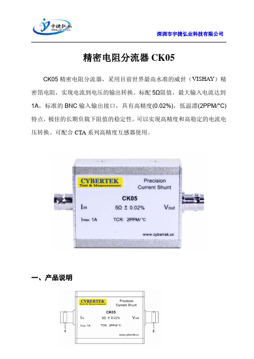
精密电阻分流器CK05
CK05精密电阻分流器,采用目前世界最高水准的威世(VISHAY)精密箔电阻,实现电流到电压的输出转换。
标配5Ω阻值,最大输入电流达到1A,标准的BNC输入输出接口,具有高精度(0.02%),低温漂(2PPM/°C)特点,极佳的长期负载下阻值的稳定性。
可以实现高精度和高稳定的电流电压转换。
可配合CTA系列高精度互感器使用。
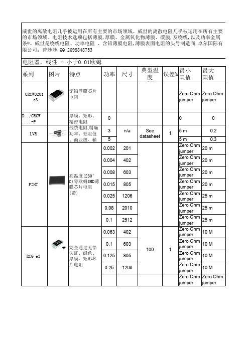
一、产品说明
1、输入接口:
BNC母头,最大输入电流1A
2、输出接口:
BNC母头,电压输出(V out=5*Iin).
二、产品附件
同轴电缆输出线(CK-310)
三、产品参数
标配阻值5Ω
精度±0.02%
温度系数2PPM/°C
最大输入工作电流1A
长期负载下阻值的稳定性±0.005%at25°C,2000小时额定负载
工作温湿度要求-20°C to40°C,80%RH or less
存储温湿度要求-40°C to60°C,80%RH or less
尺寸(长*宽*高)85mm*46mm*30mm
重量78g
四、产品使用
✧注意输入输出接口不要接反。
✧最大输入电流1A。
五、产品标配
CK05本体1个
BNC线(CK-310)1个
说明书及保修卡1册
检测报告1页。

vishay金属箔电阻参数Vishay金属箔电阻是一种重要的电子元件,被广泛应用于各类电子设备中。
它具有许多优秀的参数,如稳定性、精度、温度系数等,使其成为电路设计中不可或缺的一部分。
稳定性是金属箔电阻的重要参数之一。
稳定性指的是在一定的温度范围内,金属箔电阻的阻值变化程度。
Vishay金属箔电阻具有出色的稳定性,能够在不同的温度下保持相对稳定的阻值。
这种稳定性使得金属箔电阻能够在各种环境条件下正常工作,不受温度变化的影响。
除了稳定性,精度也是金属箔电阻的重要参数之一。
精度指的是金属箔电阻的阻值与标称阻值之间的差异程度。
Vishay金属箔电阻具有高精度,能够提供各种精度等级的产品,满足不同应用场景的需求。
高精度的金属箔电阻能够保证电路的稳定运行,提高电子设备的性能。
温度系数是金属箔电阻的另一个重要参数。
温度系数指的是金属箔电阻的阻值随温度变化的程度。
Vishay金属箔电阻具有低温度系数,能够在广泛的温度范围内保持相对稳定的阻值。
低温度系数使得金属箔电阻在高温环境下也能够正常工作,减少温度对电路性能的影响。
Vishay金属箔电阻还具有较低的噪声和良好的频率响应。
低噪声是指金属箔电阻在工作过程中产生的噪声较小,不会对电子设备的正常工作产生干扰。
良好的频率响应使得金属箔电阻能够在高频率下保持较好的性能,适用于需要高速信号处理的电路设计。
Vishay金属箔电阻还具有较高的功率承受能力和长寿命。
高功率承受能力意味着金属箔电阻能够承受较大的功率负载,不会因为过载而损坏。
长寿命使得金属箔电阻能够长时间稳定地工作,减少更换元件的频率,提高电子设备的可靠性。
Vishay金属箔电阻是一种优秀的电子元件,具有稳定性、精度、温度系数、低噪声、良好的频率响应、高功率承受能力和长寿命等优秀参数。
这些优秀的参数使得金属箔电阻成为电子设备设计中不可或缺的一部分。
无论是在通信设备、医疗仪器还是工业控制系统中,金属箔电阻都能够发挥重要作用,提高电子设备的性能和可靠性。

万联芯城VISHAY威世半导体原装进口供应,mos管,二极管,集成电路大量现货,均为原装进口库存,货源渠道为原厂及代理商。
当天报价,当天发货,一站式采购电子元器件,就上万联芯城,上万种物料型号满足采购需求,一站式报价节省采购成本!点击进入万联芯城VISHAY代理_威世代理,威世半导体 Intertechnology,Inc。
是一家美国分立半导体和无源电子元件制造商,由波兰出生的商人Felix Zandman创立。
VISHAY代理_威世代理,威世半导体在以色列,亚洲,欧洲和美洲设有制造工厂,生产整流器,二极管,MOSFET,光电子器件,精选集成电路,电阻器,电容器和电感器。
VISHAY代理_威世代理,威世半导体 Intertechnology 2011年的收入为25.94亿美元。
截至2011年12月31日,VISHAY代理_威世代理,威世半导体Intertechnology拥有约20,900名全职员工。
[1]VISHAY代理_威世代理,威世半导体 Intertechnology由波兰出生的Felix Zandman博士于1962年创立。
该公司以现代立陶宛Veisiejai 的赞德曼祖先村庄命名。
它开始运行的专利技术有两个产品线:箔电阻和箔电阻应变计。
1985年,公司从一家初创公司发展成为这些原始产品的全球领先制造商,开始进行一系列的收购,成为电子元件的广泛制造商。
[2]VISHAY代理_威世代理,威世半导体已经扩展到如此多的产品线,于2009年10月宣布将成立一家分拆公司,专注于他们在铝箔技术领域的高精密技术。
VISHAY代理_威世代理,威世半导体 Precision Group占VISHAY代理_威世代理,威世半导体年收入的约9%,其产品线包括散装金属箔电阻器,微量测量,称重传感器,过程称重和车载称重。
[3] [4] 2010年7月,VISHAY代理_威世代理,威世半导体Intertechnology完成了VISHAY代理_威世代理,威世半导体Precision Group(VPG)的分拆。

VPR220SZ (Z-Foil)Vishay Foil ResistorsUltra High Precision Z-Foil Surface Mount Power Resistors inTO-220 Configuration with TCR of ± 0.05 ppm/°C,Tolerance to ± 0.01 % and Power Rating to 8 W Foranyquestions,contact:***************Document Number: 63068Any value at any tolerance available within resistance range Model VPR220SZ, made from Vishay Bulk Metal ® Z-Foil,offers very low TCR, high stability, tight tolerance, low PCRand fast response time in a small surface mount molded resistor.The Z-Foil technology provides a significant reduction of the resistive components sensitivity to ambient temperature variations and applied power changes. Designers now can guarantee a high degree of stability and accuracy in fixed resistor applications using solutions based on Vishay’s revolutionary Z-Foil technology.Our Application Engineering Department is available to advise and make recommendations. For non-standard technical requirements and special applications, please contact us.FEATURES•Temperature Coefficient of Resistance (TCR):± 0.05 ppm/°C typical (0 °C to + 60 °C)± 0.2 ppm/°C typical (- 55 °C to + 125 °C,- 25 °C Ref.)•Tolerance: to ± 0.01 %•Power Coefficient of Resistance (PCR) “ΔR due to self heating”: 5 ppm at rated power •Electrostatic Discharge (ESD) above 25 000 V•Load Life Stability: ± 0.005 % (25 °C, 2000 hours at Rated Power)•Resistance Range: 5 Ω to 10 k Ω•Power Rating: 8 W chassis mounted (per MIL-PRF-39009)•Non Inductive, Non Capacitive Design •Current Noise: < - 40 dB•Voltage Coefficient: < 0.1 ppm/W •Non Inductive: < 0.08 µH •Non Hot Spot Design•Thermal EMF: 0.05 µV/°C typical•Terminal Finishes Available:Lead (Pb)-freeTin/Lead Alloy•For higher performances please contact usNotes1.Whichever is lower.2.Heat sink chassis dimensions and requirements perMIL-PRF-39009:3.Inductance (L) due mainly to the leads.4.The resolution limit of existing test equipment (within themeasurement capability of the equipment, or “essentially zero”).5.µV/°C relates to EMF due to lead temperature difference.Weight = 1 g Maximum Note1. Maximum specifications.* Pb containing terminations are not RoHS compliant, exemptions may apply TABLE 1 - SPECIFICATIONSLoad Life Stability at 2000 h ± 0.05 % max ΔR under full rated power at + 25 °CPower Rating at + 25 °C 8 W or 3 A 1) on heat sink 2)1.5 Wor 3 A 1) in free airFurther derating not necessary.Current Noise< 0.010 µV (rms)/V of applied voltage (- 40 dB)High Frequency Operation Rise TimeInductance 3) (L)Capacitance (C) 1 ns0.1 µH maximum: 0.03 µH typical 1.0 pF maximum: 0.5 pF typical Voltage Coefficient 4)< 0.1 ppm/V Operating Temperature Range- 55 °C to + 150 °CMaximum Working Voltage 300 V . Not to exceed power rating.Thermal EMF 5)0.15 µV/°C maximum (lead effect)DIMENSION INCHES mm L 6.00152.4W4.00101.6H 2.0050.8T0.041.0TABLE 2 - VPR220SZRESISTANCE RANGE (Ω)TIGHTEST RESISTANCE TOLERANCETCR 1)- 55 °C to + 125 °C, Ref. + 25 °C50 to 10K ± 0.01 %± 2.5 ppm/°C25 to < 50± 0.02 %10 to < 25± 0.05 %5 to < 10± 0.1 %Document Number: 63068Foranyquestions,contact:***************VPR220SZ (Z-Foil)Ultra High Precision Z-Foil Surface Mount Power Resistors in TO-220 Configuration with TCR of ± 0.05 ppm/°C, Tolerance to ± 0.01 % and Power Rating to 8 WVishay Foil ResistorsVPR220SZ (Z-Foil)Vishay Foil Resistors Ultra High Precision Z-Foil Surface Mount Power Resistorsin TO-220 Configuration with TCR of ± 0.05 ppm/°C, Tolerance to ± 0.01 % and Power Rating to 8 W Foranyquestions,contact:***************Document Number: 63068Note* For non-standard requests, please contact Application Engineering.TABLE 3 - GLOBAL PART NUMBER INFORMATIONNEW GLOBAL PART NUMBER:Y16235R00000Q9L (preferred part number format)DENOTES PRECISIONVALUE AER*YR = ΩK = k Ω0 = Standard9 = Lead (Pb)-free 1 - 999 = CustomPRODUCT CODE RESISTANCE TOLERANCEPACKAGING 1623 = VPR220SZT = ± 0.01 %Q = ± 0.02 %A = ± 0.05 %B = ± 0.1 %C = ± 0.25 %D = ± 0.5 %F = ± 1.0 %G = ± 2.0 %J = ± 5.0 %L = Bulk Pack R = T ape and ReelFOR EXAMPLE: ABOVE GLOBAL ORDER Y1623 5R00000 Q 9 L:TYPE: VPR220SZ VALUE: 5.0 ΩABSOLUTE TOLERANCE: ± 0.02 %TERMINATION: Lead (Pb)-free PACKAGING: BulkHISTORICAL PART NUMBER:VPR220SZT 5R0000Q B (will continue to be used)VPR220SZ T5R0000Q B MODEL TERMINATION OHMIC VALUERESISTANCE TOLERANCE PACKAGING VPR220SZT = Lead (Pb)-free None = Tin/Lead alloy5.0 ΩT = ± 0.01 %Q = ± 0.02 %A = ± 0.05 %B = ± 0.1 %C = ± 0.25 %D = ± 0.5 %F = ± 1.0 %G = ± 2.0 %J = ± 5.0 %B = BulkT = T ape and Reel6235000R Y 1Q 90LDisclaimer Legal Disclaimer NoticeVishayAll product specifications and data are subject to change without notice.Vishay Intertechnology, Inc., its affiliates, agents, and employees, and all persons acting on its or their behalf (collectively, “Vishay”), disclaim any and all liability for any errors, inaccuracies or incompleteness contained herein or in any other disclosure relating to any product.Vishay disclaims any and all liability arising out of the use or application of any product described herein or of any information provided herein to the maximum extent permitted by law. The product specifications do not expand or otherwise modify Vishay’s terms and conditions of purchase, including but not limited to the warranty expressed therein, which apply to these products.No license, express or implied, by estoppel or otherwise, to any intellectual property rights is granted by this document or by any conduct of Vishay.The products shown herein are not designed for use in medical, life-saving, or life-sustaining applications unless otherwise expressly indicated. Customers using or selling Vishay products not expressly indicated for use in such applications do so entirely at their own risk and agree to fully indemnify Vishay for any damages arising or resulting from such use or sale. Please contact authorized Vishay personnel to obtain written terms and conditions regarding products designed for such applications.Product names and markings noted herein may be trademarks of their respective owners.Document Number: 。
Thick Film Surface Mount Chip Resistors,Wraparound, Extremely Low Value (0.01 Ω to 0.976 Ω) For technical questions, contact: ff2cresistors@Document Number: 20019RCWEVishay DaleFEATURES•Extremely low resistance values (0.01 Ω to 0.976 Ω)•Suitable for current sensing and shunts •Metal glaze on high quality ceramic •Protective overglaze•Lead (Pb)-free solder contacts on Ni barrier layer •Compliant to RoHS directive 2002/95/EC•Halogen-free according to IEC 61249-2-21 definitionNotes•Power rating depends on the max. temperature at the solder point, the component placement density and the substrate material.•Part marking: Reference “Surface Mount Resistor Marking” (document number 20020).STANDARD ELECTRICAL SPECIFICATIONSGLOBAL MODEL POWER RATINGP 70 °C WTEMPERATURE COEFFICIENTppm/°C RESISTANCE RANGEΩE-SERIES± 1.0 %± 5.0 %RCWE04020.125± 400-0.033 to 0.0524± 2000.051 to 0.18± 1000.2 to 0.976RCWE06030.2± 700-0.010 to 0.01824± 4000.02 to 0.03± 2000.033 to 0.1± 1000.11 to 0.976RCWE08050.25± 400-0.010 to 0.01824± 3000.02 to 0.03± 2000.033 to 0.05± 1000.051 to 0.976RCWE12060.5± 600-0.010 to 0.01824± 3000.02 to 0.03± 2000.033 to 0.05± 1000.051 to 0.976RCWE1210 1.0± 500-0.010 to 0.01824± 3000.02 to 0.03± 2000.033 to 0.05± 1000.051 to 0.976RCWE2010 1.0± 600-0.010 to 0.01824± 3000.02 to 0.03± 2000.033 to 0.05± 1000.051 to 0.976RCWE2512 2.0± 600-0.010 to 0.01824± 3000.02 to 0.03± 2000.033 to 0.05± 1000.051 to 0.976GLOBAL PART NUMBER INFORMATIONPart Number: RCWE060351L0FNEAGLOBAL MODEL VALUETOLERANCE TCRPACKAGING RCWE0402RCWE0603RCWE0805RCWE1206RCWE1210RCWE2010RCWE2512L = m Ω*R = Decimal 10L0 = 0.01 ΩR470 = 0.47 Ω* use “L ” for resistancevalues < 0.1 ΩF = ± 1.0 %J = ± 5.0 %K = ± 100 ppm/°C N = ± 200 ppm/°C M = ± 300 ppm/°C Q = ± 400 ppm/°C P = ± 500 ppm/°C T = ± 600 ppm/°C G = ± 700 ppm/°CEA = Lead (Pb)-free,tape/reelW E 063510R C N 0F E L ADocument Number: 20019For technical questions, contact: ff2cresistors@RCWEThick Film Surface Mount Chip Resistors,Wraparound, Extremely Low Value (0.01 Ω to 0.976 Ω)Vishay DaleDIMENSIONSTECHNICAL SPECIFICATIONSPARAMETERUNIT RCWE0402RCWE0603RCWE0805RCWE1206RCWE1210RCWE2010RCWE2512Operating temperature range °C - 55 to + 155Maximum operating voltage V (P x R)1/2Insulation voltage U ins (1 min)V > 75> 100> 200> 300> 300> 300> 300Insulation resistance Ω> 109Weight/1000 pieces (typical)g0.735.510.517.52640.5MODELDIMENSIONS in millimetersSOLDER PAD DIMENSIONS in millimetersRESISTANCE RANGE ΩLWHT1T2a b l RCWE04020.033 to 0.976 1.05 ± 0.050.55 ± 0.050.35 ± 0.10.3 ± 0.150.25 ± 0.10.70.70.3RCWE06030.01 to 0.03 1.6 ± 0.10.85 ± 0.10.5 ± 0.10.5 ± 0.20.3 ± 0.20.9 1.00.40.033 to 0.9760.3 ± 0.20.7 1.00.8RCWE08050.01 to 0.03 2.0 ± 0.15 1.3 ± 0.10.55 ± 0.10.6 ± 0.20.35 ± 0.21.0 1.40.60.033 to 0.9760.4 ± 0.20.8 1.4 1.0RCWE12060.01 to 0.033.1 ± 0.151.6 ± 0.150.6 ± 0.10.9 ± 0.20.45 ± 0.21.31.8 1.00.033 to 0.050.8 ± 0.21.2 1.8 1.20.051 to 0.9760.45 ± 0.2 1.01.8 1.6RCWE12100.01 to 0.03 3.1 ± 0.22.5 ± 0.20.6 ± 0.10.8 ± 0.20.4 ± 0.21.32.6 1.10.033 to 0.9760.4 ± 0.20.9 2.6 2.0RCWE20100.01 to 0.035.0 ± 0.22.5 ± 0.150.6 ± 0.11.6 ± 0.30.6 ± 0.22.33.0 1.40.033 to 0.050.7 ± 0.31.4 3.0 3.20.051 to 0.9760.7 ± 0.3 1.4 3.0 3.2RCWE25120.01 to 0.036.3 ± 0.23.15 ± 0.150.6 ± 0.12.0 ± 0.30.6 ± 0.22.83.6 1.40.033 to 0.050.8 ± 0.3 1.6 3.6 3.80.051 to 0.9760.8 ± 0.31.63.63.8 For technical questions, contact: ff2cresistors@Document Number: 20019RCWEVishay DaleThick Film Surface Mount Chip Resistors,Wraparound, Extremely Low Value (0.01 Ω to 0.976 Ω)Note•Embossed carrier tape per EIA-481-1A.PERFORMANCETESTCONDITIONS OF TESTTEST LIMITS Thermal shock MIL-STD-202, method 107, - 55 °C to + 125 °C, 300 cycles at each extreme± (1.0 % + 0.0005 Ω) ΔR Short time overload 2 x rated power; duration according the model± (0.5 % + 0.0005 Ω) ΔR High temperature exposure MIL-STD-202, method 108, 1000 h at T = 125 °C, 0 % power ± (2.0 % + 0.0005 Ω) ΔR Temperature cycling JESD 22, method JA-104, 1000 cycles ( - 55 °C to + 125 °C)± (2.0 % + 0.0005 Ω) ΔR Biased humidity MIL-STD-202, method 103, 1000 h 85 °C/85 % RH, 10% x (P x R )1/2± (2.0 % + 0.0005 Ω) ΔR Mechanical shock MIL-STD-202, method 213, condition C, 10 g’s, 6 ms (half sine), 3 directions± (1.0 % + 0.0005 Ω) ΔRVibration MIL-STD-202, method 204, 5 g ’s, 20 min, 12 cycles, 3 directions, 10 Hz to 2000 Hz ± (1.0 % + 0.0005 Ω) ΔROperational lifeMIL-STD-202, method 108, 1000 h at T = 125 °C at rated power± (2.0 % + 0.0005 Ω) ΔR Resistance to solder heat MIL-STD-202, method 210, + 260 °C solder, 10 s to 12 s dwell, 25 mm/s emergence± (1.0 % + 0.0005 Ω) ΔR Moisture resistanceMIL-STD-202, method 106, 0 % power, 7a and 7b not required± (2.0 % + 0.0005 Ω) ΔRPACKAGINGMODELREELTAPE WIDTHDIAMETER PITCH PIECES/REELCODE RCWE04028 mm/punched paper 180 mm/7" 2 mm 10 000EA RCWE06038 mm/punched paper 180 mm/7" 4 mm 5000EA RCWE08058 mm/punched paper 180 mm/7" 4 mm 5000EA RCWE12068 mm/punched paper 180 mm/7" 4 mm 5000EA RCWE12108 mm/punched paper 180 mm/7" 4 mm 5000EA RCWE201012 mm/embossed plastic 180 mm/7" 4 mm 4000EA RCWE251212 mm/embossed plastic180 mm/7"8 mm2000EADisclaimer Legal Disclaimer NoticeVishayAll product specifications and data are subject to change without notice.Vishay Intertechnology, Inc., its affiliates, agents, and employees, and all persons acting on its or their behalf (collectively, “Vishay”), disclaim any and all liability for any errors, inaccuracies or incompleteness contained herein or in any other disclosure relating to any product.Vishay disclaims any and all liability arising out of the use or application of any product described herein or of any information provided herein to the maximum extent permitted by law. The product specifications do not expand or otherwise modify Vishay’s terms and conditions of purchase, including but not limited to the warranty expressed therein, which apply to these products.No license, express or implied, by estoppel or otherwise, to any intellectual property rights is granted by this document or by any conduct of Vishay.The products shown herein are not designed for use in medical, life-saving, or life-sustaining applications unless otherwise expressly indicated. Customers using or selling Vishay products not expressly indicated for use in such applications do so entirely at their own risk and agree to fully indemnify Vishay for any damages arising or resulting from such use or sale. Please contact authorized Vishay personnel to obtain written terms and conditions regarding products designed for such applications.Product names and markings noted herein may be trademarks of their respective owners.Document Number: 。
1.5KE160CA-E3/54 1.5KE47CA-E3/541.5KE6.8A thru 1.5KE540A, 1N6267A thru 1N6303AVishay General SemiconductorT RANS Z ORB ® Transient Voltage SuppressorsDEVICES FOR BI-DIRECTION APPLICATIONSFor bi-directional types, use CA suffix (e.g. 1.5KE220CA) Electrical characteristics apply in both directions.FEATURES•Glass passivated chip junction•Available in uni-directional and bi-directional •1500 W peak pulse power capability with a 10/1000 μs waveform, repetitive rate (duty cycle): 0.01 %•Excellent clamping capability •Very fast response time•Low incremental surge resistance•AEC-Q101 qualified•Solder dip 275 °C max. 10 s, per JESD 22-B106•Material categorization: for definitions of compliance please see /doc?99912TYPICAL APPLICATIONSUse in sensitive electronics protection against voltage transients induced by inductive load switching and lighting on ICs, MOSFET, signal lines of sensor units for consumer, computer, industrial, automotive, and telecommunication.MECHANICAL DATACase: molded epoxy body over passivated junction Molding compound meets UL 94 V-0 flammability rating Base P/N-E3 - RoHS compliant, commercial gradeBase P/NHE3_X - RoHS compliant, and AEC-Q101 qualified (“X” denotes revision code e.g. A, B, ...)Terminals: matte tin plated leads, solderable per J-STD-002 and JESD 22-B102E3 suffix meets JESD 201 class 1A whisker test, HE3 suffix meets JESD 201 class 2 whisker testNote• 1.5KE250A to 1.5KE540A are commercial grade only•Bi-directional is available from 1.5KE6.8CA to 1.5KE220CA onlyPolarity: For uni-directional types the color band denotes cathode end, no marking on bi-directional typesNotes(1)Non-repetitive current pulse, per fig. 3 and derated above T A= 25 °C per fig. 2(2)Measured on 8.3 ms single half sine-wave or equivalent square wave, duty cycle = 4 pulses per minute maximum (3)V F = 3.5 V for 1.5KE220A and below; V F= 5.0 V for 1.5KE250A and above PRIMARY CHARACTERISTICSV BR uni-directional 6.8 V to 540 V V BR bi-directional 6.8 V to 220 V V WM uni-directional 5.8 V to 459 V V WM bi-directional5.8 V to 185 V P PPM 1500 W P D6.5 W I FSM (uni-directional only)200 A T J max.175 °CPolarity Uni-directional, bi-directionalPackage1.5KEMAXIMUM RATINGS (T A = 25 °C unless otherwise noted)PARAMETERSYMBOL VALUE UNIT Peak pulse power dissipation with a 10/1000 μs waveform (1) (fig. 1)P PPM 1500W Peak pulse current with a 10/1000 μs waveform (1) I PPM See next tableA Power dissipation on infinite heatsink at T L = 75 °C (fig. 5)P D 6.5W Peak forward surge current 8.3 ms single half sine-wave uni-directional only (2)I FSM 200A Maximum instantaneous forward voltage at 100 A for uni-directional only (3) V F 3.5/5.0V Operating junction and storage temperature rangeT J , T STG-55 to +175°C1.5KE6.8A thru 1.5KE540A, 1N6267A thru 1N6303AVishay General SemiconductorNotes(1) Pulse test: t p≤ 50 ms (2) S urge current waveform per fig. 3 and derate per fig. 2(3) All terms and symbols are consistent with ANSI/IEEE CA62.35(4) For bi-directional types with V R 10 V and less the I Dlimit is doubled (+) Underwriters laboratory recognition for the classification of protectors (QVGQ2) under the UL standard for safety 497B and file number E136766 for both uni-directional and bi-directional devicesELECTRICAL CHARACTERISTICS (T A = 25 °C unless otherwise noted)JEDEC ® TYPE NUMBER GENERAL SEMICONDUCTOR PART NUMBER BREAKDOWN VOLTAGE V BR AT I T (1)(V) TEST CURRENT I T (mA)STAND-OFF VOLTAGE V WM (V)MAXIMUM REVERSE LEAKAGE AT V WM I D (4) (μA) MAXIMUM PEAKPULSECURRENT I PPM (2)(A)MAXIMUM CLAMPING VOLTAGE AT I PPM V C (V) MAXIMUM TEMPERATURE COEFFICIENTOF V BR (%/°C)MIN.MAX.1N6267A (+)1.5KE6.8A 6.457.1410 5.80100014310.50.0571N6268A (+)1.5KE7.5A 7.137.8810 6.4050013311.30.0611N6269A (+)1.5KE8.2A 7.798.61107.022*******.10.0651N6270A (+)1.5KE9.1A 8.659.55 1.07.785011213.40.0681N6271A (+)1.5KE10A 9.5010.5 1.08.551010314.50.0731N6272A (+)1.5KE11A 10.511.6 1.09.40 5.096.215.60.0751N6273A (+)1.5KE12A 11.412.6 1.010.2 5.089.816.70.0781N6274A (+)1.5KE13A 12.413.7 1.011.1 5.082.418.20.0811N6275A (+)1.5KE15A 14.315.8 1.012.8 1.070.821.20.0841N6276A (+)1.5KE16A 15.216.8 1.013.6 1.066.722.50.0861N6277A (+)1.5KE18A 17.118.9 1.015.3 1.059.525.20.0891N6278A (+)1.5KE20A 19.021.0 1.017.1 1.054.227.70.0901N6279A (+)1.5KE22A 20.923.1 1.018.8 1.049.030.60.0921N6280A (+)1.5KE24A 22.825.2 1.020.5 1.045.233.20.0941N6281A (+)1.5KE27A 25.728.4 1.023.1 1.040.037.50.0961N6282A (+)1.5KE30A 28.531.5 1.025.6 1.036.241.40.0971N6283A (+)1.5KE33A 31.434.7 1.028.2 1.032.845.70.0981N6284A (+)1.5KE36A 34.237.8 1.030.8 1.030.149.90.0991N6285A (+)1.5KE39A 37.141.0 1.033.3 1.027.853.90.1001N6286A (+)1.5KE43A 40.945.2 1.036.8 1.025.359.30.1011N6287A (+)1.5KE47A 44.749.4 1.040.2 1.023.164.80.1011N6288A (+)1.5KE51A 48.553.6 1.043.6 1.021.470.10.1021N6289A (+)1.5KE56A 53.258.8 1.047.8 1.019.577.00.1031N6290A (+)1.5KE62A 58.965.1 1.053.0 1.017.685.00.1041N6291A (+)1.5KE68A 64.671.4 1.058.1 1.016.392.00.1041N6292A (+)1.5KE75A 71.378.8 1.064.1 1.014.61040.1051N6293A (+)1.5KE82A 77.986.1 1.070.1 1.013.31130.1051N6294A (+)1.5KE91A 86.595.5 1.077.8 1.012.01250.1061N6295A (+)1.5KE100A 95.0105 1.085.5 1.010.91370.1061N6296A (+)1.5KE110A 105116 1.094.0 1.09.91520.1071N6297A (+)1.5KE120A 114126 1.0102 1.09.11650.1071N6298A (+)1.5KE130A 124137 1.0111 1.08.41790.1071N6299A (+)1.5KE150A 143158 1.0128 1.07.22070.1061N6300A (+)1.5KE160A 152168 1.0136 1.0 6.82190.1081N6301A (+)1.5KE170A 162179 1.0145 1.0 6.42340.1081N6302A (+)1.5KE180A 171189 1.0154 1.0 6.12460.1081N6303A (+)1.5KE200A 190210 1.0171 1.0 5.52740.108-(+)1.5KE220A 209231 1.0185 1.0 4.63280.108- 1.5KE250A 237263 1.0214 1.0 4.43440.110- 1.5KE300A 285315 1.0256 1.0 3.64140.110- 1.5KE350A 333368 1.0300 1.0 3.14820.110- 1.5KE400A 380420 1.0342 1.0 2.75480.110- 1.5KE440A 418462 1.0376 1.0 2.56020.110- 1.5KE480A 456504 1.0408 1.0 2.286580.110- 1.5KE510A 485535 1.0434 1.0 2.156980.110- 1.5KE540A 513567 1.0459 1.0 2.037400.1101.5KE6.8A thru 1.5KE540A, 1N6267A thru 1N6303A Vishay General Semiconductor Notes(1)AEC-Q101 qualified(2)Applied for 1.5KE6.8AHE3_A to 1.5KE220AHE3_A, and 1.5KE6.8CAHE3_A to 1.5KE220CAHE3_ARATINGS AND CHARACTERISTICS CURVES (T A = 25 °C unless otherwise noted)Fig. 1 - Peak Pulse Power Rating CurveFig. 2 - Pulse Power or Current vs. Initial Junction TemperatureFig. 3 - Pulse WaveformFig. 4 - Typical Junction CapacitanceTHERMAL CHARACTERISTICS (T A = 25 °C unless otherwise noted)PARAMETER SYMBOL VALUE UNIT Typical thermal resistance, junction to ambient RθJA75°C/ W Typical thermal resistance, junction to lead RθJL15.4ORDERING INFORMATION (Example)PREFERRED PIN UNIT WEIGHT (g)PREFERRED PACKAGE CODE BASE QUANTITY DELIVERY MODE1.5KE6.8A-E3/540.96854140013" diameter paper tape and reel 1.5KE6.8AHE3_A/C (1)(2)0.968C140013" diameter paper tape and reel1.5KE6.8A thru 1.5KE540A, 1N6267A thru 1N6303A Vishay General SemiconductorFig. 5 - Power Derating CurveFig. 6 - Maximum Non-Repetitive Forward Surge CurrentUni-Directional onlyFig. 7 - Incremental Clamping Voltage Curve (Uni-Directional)Fig. 8 - Incremental Clamping Voltage Curve (Uni-directional) Fig. 9 - Incremental Clamping Voltage Curve (Bi-directional) Fig. 10 - Incremental Clamping Voltage Curve (Bi-Directional)1.5KE6.8A thru 1.5KE540A, 1N6267A thru 1N6303A Vishay General SemiconductorFig. 11 - Instantaneous Forward Voltage Characteristics Curve Fig. 12 - Typical Transient Thermal Impedance PACKAGE OUTLINE DIMENSIONS in inches (millimeters)APPLICATION NOTES•This series of Silicon Transient Suppressors is used in applications where large voltage transients can permanently damage voltage-sensitive components.•The TVS diode can be used in applications where induced lightning on rural or remote transmission lines presents a hazard to electronic circuitry (ref: R.E.A. specification P.E. 60). •This Transient Voltage Suppressor diode has a pulse power rating of 1500 W for 1 ms. The response time of TVS diode clamping action is effectively instantaneous (1 x 10⁻⁹ s bi-directional); therefore, they can protect integrated circuits, MOS devices, hybrids, and other voltage sensitive semiconductors and components. TVS diodes can also be used in series or parallel to increase the peak power ratings.Legal Disclaimer Notice VishayDisclaimerALL PRODUCT, PRODUCT SPECIFICAT IONS AND DAT A ARE SUBJECT T O CHANGE WIT HOUT NOT ICE T O IMPROVE RELIABILITY, FUNCTION OR DESIGN OR OTHERWISE.Vishay Intertechnology, Inc., its affiliates, agents, and employees, and all persons acting on its or their behalf (collectively, “Vishay”), disclaim any and all liability for any errors, inaccuracies or incompleteness contained in any datasheet or in any other disclosure relating to any product.Vishay makes no warranty, representation or guarantee regarding the suitability of the products for any particular purpose or the continuing production of any product. To the maximum extent permitted by applicable law, Vishay disclaims (i) any and all liability arising out of the application or use of any product, (ii) any and all liability, including without limitation special, consequential or incidental damages, and (iii) any and all implied warranties, including warranties of fitness for particular purpose, non-infringement and merchantability.Statements regarding the suitability of products for certain types of applications are based on Vishay’s knowledge of typical requirements that are often placed on Vishay products in generic applications. Such statements are not binding statements about the suitability of products for a particular application. It is the customer’s responsibility to validate that a particular product with the properties described in the product specification is suitable for use in a particular application. Parameters provided in datasheets and / or specifications may vary in different applications and performance may vary over time. All operating parameters, including typical parameters, must be validated for each customer application by the customer’s technical experts. Product specifications do not expand or otherwise modify Vishay’s terms and conditions of purchase, including but not limited to the warranty expressed therein.Except as expressly indicated in writing, Vishay products are not designed for use in medical, life-saving, or life-sustaining applications or for any other application in which the failure of the Vishay product could result in personal injury or death. Customers using or selling Vishay products not expressly indicated for use in such applications do so at their own risk. Please contact authorized Vishay personnel to obtain written terms and conditions regarding products designed for such applications.No license, express or implied, by estoppel or otherwise, to any intellectual property rights is granted by this document or by any conduct of Vishay. Product names and markings noted herein may be trademarks of their respective owners.© 2017 VISHAY INTERTECHNOLOGY, INC. ALL RIGHTS RESERVED1.5KE160CA-E3/54 1.5KE47CA-E3/54。
ASVMP• Storage Area Networks(SATA, SAS, Fiber Channel)• Passive Optical Networks (EPON, 10G-EPON, GPON, 10G-PON)• Ethernet (1G, 10GBASE-T,/KR/LR/SR, FCoE • PCI Express • Display port• Low Power Consumption for high speed communication • Exceptional Stability Over Temp. at -40 to +85°C, ±15ppm• Extended Automotive Grade Temp. stability at -55 to +125°C, ±25ppm • Available in 50kG Shock Resistance Configuration upon request • MIL-STD-883 shock and vibration compliant • Durable QFN Plastic Compact Packaging • Standby or Disable Tri-state function• Low jitter (Period jitter RMS and Phase jitter RMS)• High power supply noise reduction, -50dBcLow Jitter High Performance Moisture Sensitivity Level – MSL 1Common Key Electrical Specifications – CMOS, LVPECL, LVDS, and HCSL* For 2.3000MHz < F0 < 9.9999MHz, 6-8 weeks lead-time applies Key Electrical Specifications – CMOSFrequency RangeCMOS 2.3000* 170.0000 MHzCMOS3.3000* 170.0000 LVPECL 2.3000* 460.0000 Commercial, Industrial temp. rangeLVDS 2.3000* 460.0000 Commercial, Industrial temp rangeHCSL2.3000*460.0000Commercial, Industrial temp. rangeOperating Temperature -20 +70 °C See optionsC ° 051+ 55-e r u t a r e p m e T e g a r o t S Overall Frequency Stability -50 +50 ppm See options Supply Voltage (Vdd) +2.25 +3.6 Vs m 5 e m i T p u t r a t S Enable Time 20 ns STD (Tri-state)5 ms PD option (Power Down)s n 5 e m i T e l b a s i D Disable Current20 22 mA STD (Tri-state)0.095 PD option (Power Down)Tri-state Function (Standby/Disable) "1" (VIH 0.75*Vdd) or Open: Oscillation "0" (VIL<0.25*Vdd) : Hi ZV 40k pull-up resister embeddedr a e y t s r i F m p p0.5+ 0.5-g n i g A Supply Current (I dd ) 31 35 mA CL=15pF, 125MHz Output Logic Level V OH 0.9*V ddV I=±6mA V OL 0.1*V dd V Rise Time Tr 1.1 2.0 ns CL=15pF 20% to 80%Fall Time Tf1.32.0 ns% 55 54e l c y C y t u D Integrated Phase Jitter (J PH ) 0.30 2 ps 200kHz ~ 20MHz@125MHz 0.38 2 100kHz ~ 20MHz@125MHz 1.70 2 12kHz ~ 20MHz@125MHzPeriod Jitter RMS (J PERs p0.3)PbRoHS/RoHS II compliant7.0 x 5.0 x 0.85mm-20 ~ +70°C -40 ~ +85°C -40 ~ +105°C -55 ~ +125°CKey Electrical Specifications – LVPECLKey Electrical Specifications – LVDS NotesSupply Current (I dd)56.5 58 mA RL=50 Output Logic Level V OH V dd-1.08 V RL=50V OL V dd-1.55 VPeak to Peak Output Swing (V pp) 800 mV Single endedRise Time Tr 250ps RL=50 , CL=0pFFall Time Tf 250l a i t n e r e f f i D%2584e l c y Cy t u DIntegrated Phase Jitter (J PH) 0.25 2ps200kHz ~ 20MHz@156.25MHz0.38 2 100kHz ~ 20MHz@156.25MHz1.70 2 12kHz ~ 20MHz@156.25MHzPeriod Jitter RMS (J PER s p5.2)Notes Supply Current (I dd)29 32 mA RL=100Output Offset Voltage (V OS) 1.125 1.4 V RL=100 differential Delta Offset Voltage (V OS) 50 mVPeak to Peak Output Swing (V pp) 350 mV Single endedRise Time Tr 200ps RL=50 , CL=2pFFall Time Tf 200l a i t n e r e f f i D%2584e l c y Cy t u DIntegrated Phase Jitter (J PH) 0.28 2ps200kHz ~ 20MHz@156.25MHz0.40 2 100kHz ~ 20MHz@156.25MHz1.70 2 12kHz ~ 20MHz@156.25MHzPeriod Jitter RMS (J PER s p5.2)Key Electrical Specifications – HCSLNotes Supply Current (I dd)40 42 mA RL=50Output Logic Level V OH0.725 V RL=50V OL0.1 V Peak to Peak Output Swing (V pp) 750 mV Single endedRise Time Tr 200 400ps RL=50 , CL=2pFFall Time Tf 200 400l a i t n e r e f f i D%2584e l c y Cy t u DIntegrated Phase Jitter (J PH) 0.25 2ps200kHz ~ 20MHz@156.25MHz0.37 2 100kHz ~ 20MHz@156.25MHz1.70 2 12kHz ~ 20MHz@156.25MHzPeriod Jitter RMS (J PER s p5.2)20% to 80% 20% to 80% 20% to 80%Absolute Maximum RatingsSupply Voltage -0.3 +4.0 VInput Voltage -0.3 V dd+0.3 VJunction Temp. +150 °CStorage Temp. -55 +150 °CSoldering Temp. +260 °C 40sec maxESDHBM MM CDM 4,0004001,500VCMOS OUTPUTTest Circuit(Unless specified otherwise: T=25° C, VDD=3.3 V) LVPECL outputTest CircuitASVMPTest CircuitLVDS OUTPUTHCSL OUTPUTASVMPPbRoHS/RoHS II compliantTest Circuit7.0 x 5.0 x 0.85mmASVMPASVMPFunction Tri-state NC GND Output NC (CMOS)Output (LVPECL, LVDS, HCSL)VddNote: Recommend using an approximately 0.01uF bypass capacitor between PIN 6and 3.Center pad: NC / GNDRecommended Land Pattern for CMOSRecommended Land Pattern for LVPECL, LVDS, HCSLPbRoHS/RoHS II compliant7.0 x 5.0 x 0.85mm6413ASVMPTube: 50pcs/tubeUnit orientation in tube:Dimensions: mmPbRoHS/RoHS II compliant7.0 x 5.0 x 0.85mm。
Document Number: 28707For technical questions, contact: specialresistors@MMU 0102 VG03, MMA 0204 VG03, MMB 0207 VG03Vishay BeyschlagMELF Resistors with Established ReliabilityMMU 0102 VG03, MMA 0204 VG03 and MMB 0207 VG03thin film MELF resistors with established reliability are the perfect choice for all high-reliability applications typically found in the fields of military, aircraft and spacecraft electronics. These versions supplement the families of professional and precision MELF resistors MMU 0102, MMA 0204 and MMB 0207.FEATURES•Approved to EN 140401-803, version E •Established reliability, failure rate level E6•Advanced metal film technology•Excellent overall stability: Exceeds class 0.25•F orce fitted steel caps, tin plated on nickel barrier•Pure Sn termination on Ni barrier layer•Compatible with lead (Pb)-free and lead containing soldering processes•Compliant to RoHS directive 2002/95/ECAPPLICATIONS•Medical •Military •AerospaceNotes•These resistors do not feature a limited lifetime when operated within the permissible limits. However, resistance value drift increasing over operating time may result in exceeding a limit acceptable to the specific application, thereby establishing a functional lifetime•The failure rate level E6 (10-6/h, πQ = 0,3), corresponding to MIL Level P, is superior to level E5 (10-5/h, πQ = 1) and thus may be used as a replacement(1)These figures provide a user advantage over the prescriptions or requirements of EN 140401-803.METRIC SIZEDIN:010*********EN/CECC:RC2211MRC3715MRC6123MTECHNICAL SPECIFICATIONSDESCRIPTION MMU 0102 VG03MMA 0204 VG03MMB 0207 VG03EN/CECC size, style RC2211M RC3715M RC6123M Resistance range 100Ωto 2.21M Ω1Ωto 5.11M Ω1Ωto 10M ΩResistance tolerance ± 1 %; ± 0.1 %T emperature coefficient± 50ppm/K; ± 15 ppm/KClimatic category (LCT/UCT/duration)55/125/56Rated dissipation, P 700.2W 0.25W 0.4W Operating voltage, U max. AC/DC 150V 200V 300V Film temperature125°C Max. resistance change at P 70for resistance range, |ΔR /R| after:100Ωto 221k Ω1Ωto 332k Ω1Ωto 1M Ω1000h ≤ 0.15 % (1)8000h ≤ 0.3 % (1)225000h≤ 1 %Permissible voltage against ambient (insulation):1 min; U ins 200V 300V 500V Continuous75V75V 75VAssessed failure rate levelE6 = 10-6/hQuality factor, πQ0.3Failure rate: FIT observed< 0.1 x 10⁻⁹/h For technical questions, contact: specialresistors@Document Number: 28707MMU 0102 VG03, MMA 0204 VG03, MMB 0207 VG03Vishay BeyschlagMELF Resistors with Established ReliabilityNote•Products can be ordered using either the PART NUMBER or the PRODUCT DESCRIPTIONPART NUMBER AND PRODUCT DESCRIPTIONPART NUMBER: MMA0204WC4999FB300PART NUMBER: MMA0204WZ0000ZB300MODEL/SIZE SPECIFICATION TCR VALUE TOLERANCE PACKAGINGMMU 0102MMA 0204MMB 0207W = EN 140401-803;failure rate level E6C = ± 50 ppm/K E = ± 15 ppm/K Z = Jumper3 digit value 1 digit multiplier MULTIPLIER 8 = *10-29 = *10-10 = *1001 = *1012 = *1023 = *1034 = *1045 = *1050000 = JumperF = ± 1 %B = ± 0.1 %Z = JumperB1B3B0B2B7M3M8PRODUCT DESCRIPTION: MMA 0204-50 1% VG03 BL 49R9PRODUCT DESCRIPTION: MMA 0204 VG03 BL 0R0MMA 0204-50 1 %VG03BL 49R9MMA 0204--VG03BL 0R0MODEL/SIZE TCR T OLERANCE SPECIFICATION PACKAGINGRESISTANCE VALUE MMU 0102MMA 0204MMB 0207± 50 ppm/K ± 15 ppm/K± 1 %± 0.1 %VG03 = EN 140401-803;failure rate level E6B1BL B0B2B7M3M849R9 = 49.9 Ω4K64 = 4.64 k Ω0R0 = JumperMMA24WZ 000ZB30M M A 0204W C 4999F B 300Document Number: 28707For technical questions, contact: specialresistors@MMU 0102 VG03, MMA 0204 VG03, MMB 0207 VG03MELF Resistors with Established ReliabilityVishay BeyschlagNote•The ordering information according to EN 140401-803:2007 shown above succeeds and replaces the ordering information according to earlier versions of the detail specification EN 140401-803 or its predecessor CECC 40401-803, for example:CECC 40401-803 EZ RC3715M C 49R9 F E6CECC 40401-803 S RC3715 C 49R9 F E6with EZ; S Assessment level, where EZ is successor to and superior replacement for SRC3715M; RC3715Style, with added suffix M for “metric”C Temperature coefficient, according to the detail specificationC = ± 50 ppm/K; E = ± 15 ppm/KNote•According to EN 140401-803, resistance values are to be selected from the E96 series for ± 1 % tolerance and from the E192 series for ±0.1 % toleranceEN 140401-803 ORDERING INFORMATIONExample of the ordering information for a resistor: MMA 0204-50 1 % VG03 49R9EN140401-803EZRC3715MR49R9FE6Example of the ordering information for a zero ohm jumper: MMA 0204 VG03 0R0EN140401-803EZRC3715M-0R00-E6The elements used in the component number have the following meaning:EN140401-803EZRC3715M R 49R9F E6EN detail specification numberAssessment level for the zero-defect approach StyleT emperature coefficient, according to EN 60062R = ± 50 ppm/K; P = ± 15 ppm/KResistance value, according to EN 60062, 4 characters T olerance on rated resistance, according to EN 60062F = ± 1 %; B = ± 0.1 %Failure rate level according to EN 60115-1, table ZB.1TEMPERATURE COEFFICIENT AND RESISTANCE RANGEDESCRIPTIONRESISTANCE VALUETCR TOLERANCEMMU 0102 VG03MMA 0204 VG03MMB 0207 VG03± 50 ppm/K ± 1 %100Ωto 2.21 M Ω1Ωto 5.11 M Ω1Ωto 10 M Ω± 15 ppm/K± 0.1 %100Ωto 100 k Ω75Ωto 100 k Ω75Ωto 499k ΩJumper≤ 10m Ω; I max. = 2 A≤ 10m Ω; I max. = 3 A≤ 10m Ω; I max. = 5 APACKAGINGMODELANTISTATIC BLISTER TAPE ON REELACC. IEC 60286-3, TYPE IIBULK CASE ACC. IEC 60286-6UNIT QUANTITYCODE QUANTITYCODEMMU 0102 VG03180 mm/7"1000B18 000M83000B3 = BL 330 mm/13"10 000B0MMA 0204 VG03180 mm/7"1000B1 3 000M33000B3 = BL 330 mm/13"10 000B0MMB 0207 VG03180 mm/7"1000B1-2000B2330 mm/13"7000B7 For technical questions, contact: specialresistors@Document Number: 28707MMU 0102 VG03, MMA 0204 VG03, MMB 0207 VG03Vishay BeyschlagMELF Resistors with Established ReliabilityDIMENSIONSNote•Color code marking is applied according to IEC 60062 (3) in five bands. Each color band appears as a single solid line, voids are permissible if at least 2/3 of the band is visible from each radial angle of view. The last color band for tolerance is approximately 50 % wider than the other bands. An interrupted blue band between the 1st and 2nd full band indicates the failure rate level E6. An interrupted orange band between the 4th and 5th full band indicates the temperature coefficient of 15 ppm/K.Note•The given solder pad dimensions reflect the considerations for board design and assembly as outlined e.g. in standards IEC 61188-5-x, or in publication IPC 7351. They do not guarantee any supposed thermal properties, however, they will be found adequate for most general applications.DIMENSIONS AND MASSTYPEL (mm)D (mm)L 1 min.(mm)D 1(mm)K (mm)MASS (mg)MMU 0102 VG03 2.2 + 0/- 0.1 1.1 + 0/- 0.1 1.2 D + 0/- 0.10.4 ± 0.057MMA 0204 VG03 3.6 + 0/- 0.2 1.4 + 0/- 0.1 1.8 D + 0/- 0.150.8 ± 0.119MMB 0207 VG035.8 + 0/- 0.152.2 + 0/- 0.23.2D + 0/- 0.21.15 ± 0.179RECOMMENDED SOLDER PAD DIMENSIONSTYPEWAVE SOLDERINGREFLOW SOLDERING G (mm)Y (mm)X (mm)Z (mm)G (mm)Y (mm)X (mm)Z (mm)MMU 0102 VG030.7 1.2 1.5 3.1 1.10.8 1.3 2.7MMA 0204 VG03 1.5 1.5 1.8 4.5 1.7 1.2 1.6 4.1MMB 0207 VG032.82.12.67.03.21.72.46.6D DMMU 0102 VG03, MMA 0204 VG03, MMB 0207 VG03 MELF Resistors with Established Reliability Vishay BeyschlagDESCRIPTIONProduction is strictly controlled and follows an extensive set of instructions established for reproducibility. A homogeneous film of metal alloy is deposited on a high grade ceramic body (Al2O3) and conditioned to achieve the desired temperature coefficient. Nickel plated steel termination caps are firmly pressed on the metallized rods. A special laser is used to achieve the target value by smoothly cutting a helical groove in the resistive layer without damaging the ceramics. The resistor elements are covered by a protective coating designed for electrical, mechanical and climatic protection. The terminations receive a final pure tin on nickel plating.F ive color code rings designate the resistance value and tolerance in accordance with IEC 60062 (3).The result of the determined production is verified by an extensive testing procedure performed on 100 % of the individual resistors. Only accepted products are laid directly into the blister tape in accordance with IEC 60286-3 (3), Type II or bulk case in accordance with IEC 60286-6 (3).ASSEMBLYThe resistors are suitable for processing on automatic SMD assembly systems. They are suitable for automatic soldering using wave, reflow or vapour phase as shown in IEC61760-1 (3). Solderability is specified for 2 years after production or requalification, however, excellent solderability is proven after extended storage in excess of 10 years. The permitted storage time is 20 years.The resistors are completely lead (Pb)-free, the pure tin plating provides compatibility with lead (Pb)-free soldering processes. The immunity of the plating against tin whisker growth has been proven under extensive testing.The encapsulation is resistant to all cleaning solvents commonly used in the electronics industry, including alcohols, esters and aqueous solutions. The suitability of conformal coatings, if applied, shall be qualified by appropriate means to ensure the long-term stability of the whole system.All products comply with the GADSL(1) and the CEFIC-EECA-EICTA(2) list of legal restrictions on hazardous substances. This includes full compliance with the following directives:•2000/53/EC End of Vehicle Life Directive (ELV) and Annex II (ELV II)•2002/95/EC Restriction of the use of Hazardous Substances directive (RoHS)•2002/96/EC Waste Electrical and Electronic Equipment Directive (WEEE)APPROVALSThe resistors are approved within the IECQ-CECC Quality Assessment System for Electronic Components to the detail specification EN140401-803 which refers to EN60115-1, EN140400 and the variety of environmental test procedures of the IEC 60068 (3)series.Conformity is attested by the use of the CECC Logo () as the Mark of Conformity on the package label.Vishay BEYSCHLAG has achieved “Approval of Manufacturer” in accordance with IEC QC001002-3, clause 2. The release certificate for “Technology Approval Schedule” in accordance with CECC240001 based on IEC QC001002-3, clause 6 is granted for the Vishay BEYSCHLAG manufacturing process.RELATED PRODUCTSThis product family of thin film MELF resistors with established reliability is complemented by Zero Ohm Jumpers.A wider range of TCR, tolerance and resistance values, plus the option of values from a different E series is available with products approved to EN 140401-803, Version A, without established reliability, nominal failure rate level E0 (quality factor πQ = 3). See the datasheets:•“Professional MELF Resistors”, document no. 28713•“Precision MELF Resistors”, document no. 28714•“High Precision MELF Resistor”, document no. 28715Notes(1)Global Automotive Declarable Substance List, see (2)CEFIC (European Chemical Industry Council), EECA (European Electronic Component Manufacturers Association), EICTA (European tradeorganisation representing the information and communications technology and consumer electronics), see → issues →environment policy → chemicals → chemicals for electronics(3)The quoted IEC standards are also released as EN standards with the same number and identical contentsDocument Number: 28707for technical questions, contact: specialresistors@ MMU 0102 VG03, MMA 0204 VG03, MMB 0207 VG03Vishay Beyschlag MELF Resistors with Established ReliabilityFUNCTIONAL PERFORMANCE For technical questions, contact: specialresistors@ Document Number: 28707MMU 0102 VG03, MMA 0204 VG03, MMB 0207 VG03 MELF Resistors with Established Reliability Vishay BeyschlagFUNCTIONAL PERFORMANCEFurther information on the performance of these products is given in the following datasheets:•“Professional MELF Resistors”, document no. 28713•“Precision MELF Resistors”, document no. 28714TESTS AND REQUIREMENTSAll tests are carried out in accordance with the following specifications:EN 60115-1, generic specificationEN 140400, sectional specificationEN 140401-803, detail specificationF or further information on the tests and requirements of these products please refer to the specifications mentioned above, and to the following datasheets:•“Professional MELF Resistors”, document no. 28713•“Precision MELF Resistors”, document no. 28714HISTORICAL 12NC INFORMATIONNoteThe 12NC numeric codes are no longer supported as an official Vishay ordering code. However, customers using the 12NC in their material management system may choose to use the 12NC as their customer specific part numbering system.•The resistors had a 12-digit numeric code starting with 2312•The subsequent 4digits indicated the resistor type, specification and packaging; see the 12NC table•The remaining 4digits indicated the resistance value:-The first 3digits indicate the resistance value-The last digit indicated the resistance decade in accordance with the resistance decade table RESISTANCE DECADEHistorical 12NC ExampleThe 12NC of a MMU 0102 VG03 resistor, value 287K and TCR 50 with ± 1 % tolerance, supplied in blister tape of 3000units per reel was: 2312 165 02874.RESISTANCE DECADE LAST DIGIT1Ω to9.99Ω810Ω to99.9Ω9100Ω to999Ω11 kΩto9.99kΩ210kΩ to99.9kΩ3100kΩ to999kΩ41MΩ to9.99MΩ510MΩ6HISTORICAL 12NC - Resistor type and packagingDESCRIPTION2312........BLISTER TAPE ON REEL BULK CASETYPE TCR TOL.B11000 PIECESBL3000 PIECESB010 000 PIECESM88000 PIECESMMU 0102 VG03± 50 ppm/K± 1 %170 0....165 0....175 0....060 0....± 15 ppm/K± 0.1 %172 0....167 0....177 0....062 0....Jumper172 90001167 90001177 90001062 90001TYPE TCR TOL.B11000 PIECESBL3000 PIECESB010 000 PIECESM33000 PIECESMMA 0204 VG03± 50 ppm/K± 1 %140 0....155 0....145 0....040 0....± 15 ppm/K± 0.1 %142 0....157 0....147 0....042 0....Jumper142 90001157 90001147 90001042 90001TYPE TCR TOL.B11000 PIECESB22000 PIECESB77000 PIECES-MMB 0207 VG03± 50 ppm/K± 1 %180 0....195 0....185 0....± 15 ppm/K± 0.1 %182 0....197 0....187 0....Jumper182 ******** 90001187 90001Document Number: 28707for technical questions, contact: specialresistors@ VishayDisclaimerAll product specifications and data are subject to change without notice.Vishay Intertechnology, Inc., its affiliates, agents, and employees, and all persons acting on its or their behalf (collectively, “Vishay”), disclaim any and all liability for any errors, inaccuracies or incompleteness contained herein or in any other disclosure relating to any product.Vishay disclaims any and all liability arising out of the use or application of any product described herein or of any information provided herein to the maximum extent permitted by law. The product specifications do not expand or otherwise modify Vishay’s terms and conditions of purchase, including but not limited to the warranty expressed therein, which apply to these products.No license, express or implied, by estoppel or otherwise, to any intellectual property rights is granted by this document or by any conduct of Vishay.The products shown herein are not designed for use in medical, life-saving, or life-sustaining applications unless otherwise expressly indicated. Customers using or selling Vishay products not expressly indicated for use in such applications do so entirely at their own risk and agree to fully indemnify Vishay for any damages arising or resulting from such use or sale. Please contact authorized Vishay personnel to obtain written terms and conditions regarding products designed for such applications.Product names and markings noted herein may be trademarks of their respective owners.Document Number: VishayDisclaimerALL PRODU CT, PRODU CT SPECIFICATIONS AND DATA ARE SU BJECT TO CHANGE WITHOU T NOTICE TO IMPROVE RELIABILITY, FUNCTION OR DESIGN OR OTHERWISE.Vishay Intertechnology, Inc., its affiliates, agents, and employees, and all persons acting on its or their behalf (collectively,“Vishay”), disclaim any and all liability for any errors, inaccuracies or incompleteness contained in any datasheet or in any other disclosure relating to any product.Vishay makes no warranty, representation or guarantee regarding the suitability of the products for any particular purpose or the continuing production of any product. To the maximum extent permitted by applicable law, Vishay disclaims (i) any and all liability arising out of the application or use of any product, (ii) any and all liability, including without limitation special, consequential or incidental damages, and (iii) any and all implied warranties, including warranties of fitness for particular purpose, non-infringement and merchantability.Statements regarding the suitability of products for certain types of applications are based on Vishay’s knowledge of typical requirements that are often placed on Vishay products in generic applications. Such statements are not binding statements about the suitability of products for a particular application. It is the customer’s responsibility to validate that a particular product with the properties described in the product specification is suitable for use in a particular application. Parameters provided in datasheets and/or specifications may vary in different applications and performance may vary over time. All operating parameters, including typical parameters, must be validated for each customer application by the customer’s technical experts. Product specifications do not expand or otherwise modify Vishay’s terms and conditions of purchase, including but not limited to the warranty expressed therein.Except as expressly indicated in writing, Vishay products are not designed for use in medical, life-saving, or life-sustaining applications or for any other application in which the failure of the Vishay product could result in personal injury or death. Customers using or selling Vishay products not expressly indicated for use in such applications do so at their own risk and agree to fully indemnify and hold Vishay and its distributors harmless from and against any and all claims, liabilities, expenses and damages arising or resulting in connection with such use or sale, including attorneys fees, even if such claim alleges that Vishay or its distributor was negligent regarding the design or manufacture of the part. Please contact authorized Vishay personnel to obtain written terms and conditions regarding products designed for such applications.No license, express or implied, by estoppel or otherwise, to any intellectual property rights is granted by this document or by any conduct of Vishay. Product names and markings noted herein may be trademarks of their respective owners.Material Category PolicyVishay Intertechnology, Inc. hereb y certifies that all its products that are identified as RoHS-Compliant fulfill the definitions and restrictions defined under Directive 2011/65/EU of The European Parliament and of the Council of June 8, 2011 on the restriction of the use of certain hazardous substances in electrical and electronic equipment (EEE) - recast, unless otherwise specified as non-compliant.Please note that some Vishay documentation may still make reference to RoHS Directive 2002/95/EC. We confirm that all the products identified as being compliant to Directive 2002/95/EC conform to Directive 2011/65/EU.Revision: 12-Mar-121Document Number: 91000。