IMPROVEMENT OF DEFECT CHARACTERIZATION WITU ULTRASONIC ADAPTIVE FOCUSINC TECHNIQUE- THE FAU
- 格式:pdf
- 大小:1.74 MB
- 文档页数:7
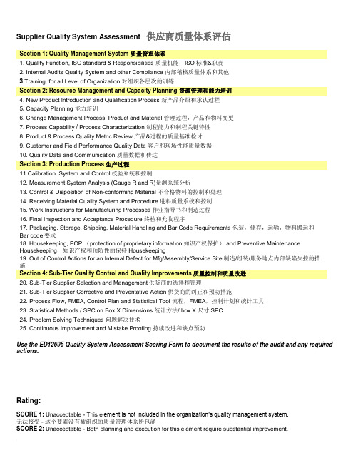
Supplier Quality System Assessment 供应商质量体系评估Section 1: Quality Management System 质量管理体系1. Quality Function, ISO standard & Responsibilities 质量机能,ISO标准&职责2. Internal Audits Quality System and other Compliance 内部稽核质量体系和其他3.Training for all Level of Organization 对组织各层次的训练Section 2: Resource Management and Capacity Planning 资源管理和能力培训4. New Product Introduction and Qualification Process 新产品介绍和承认过程5. Capacity Planning 能力培训6. Change Management Process, Product and Material 管理过程,产品和物料变更7. Process Capability / Process Characterization 制程能力和制程关键特性8. Product & Process Quality Metric Review 产品&过程的质量基准检讨9. Customer and Field Performance Quality Data 客户和现场性能质量数据10. Quality Data and Communication 质量数据和传达Section 3: Production Process生产过程11.Calibration System and Control校验系统和控制12. Measurement System Analysis (Gauge R and R)量测系统分析13. Control & Disposition of Non-conforming Material 不合格物料的控制和处理14. Receiving Material Quality System and Procedure进料质量系统和控制15. Work Instructions for Manufacturing Processes 作业指导书和制造过程16. Final Inspection and Acceptance Procedure 终检和允收程序17. Packaging, Storage, Shipping, Material Handling and Bar Code Requirements 包装,储存,运输,物料搬运和Bar code要求18. Housekeeping, POPI(protection of proprietary information 知识产权保护) and Preventive Maintenance Housekeeping,知识产权和预防性的保持Housekeeping19. Out of Control Actions for an Internal Defect for Mfg/Assembly/Service Site制造/组装/服务地点内部缺陷失控的措施Section 4: Sub-Tier Quality Control and Quality Improvements质量控制和质量改进20. Sub-Tier Supplier Selection and Management供货商的选择和管理21. Sub-Tier Supplier Corrective and Preventative Action供货商的纠正和预防措施22. Process Flow, FMEA, Control Plan and Statistical Tool 流程,FMEA,控制计划和统计工具23. Statistical Methods / SPC on Box X Dimensions 统计方法/ box X 尺寸SPC24. Problem Solving Techniques 问题解决技术25. Continuous Improvement and Mistake Proofing 持续改进和缺点预防Use the ED12695 Quality System Assessment Scoring Form to document the results of the audit and any required actions.Rating:SCORE 1: Unacceptable - This e lement is not included in the organization’s quality management system.无法接受 - 这个要素没有被组织的质量管理体系所包涵SCORE 2: Unacceptable - Both planning and execution for this element require substantial improvement.无法接受 - 这个要素的计划和执行都需要进一步改进SCORE 3: Marginally Acceptable - This element is included in the supplier’s quality management system and planning is adequate. However, execution requires improvement.边缘接受 - 此要素包含于供货商的质量体系,计划比较完善。

位错缠结英文术语Dislocation EntanglementDislocation is a fundamental concept in the field of materials science and solid mechanics, as it plays a crucial role in the understanding and prediction of the mechanical properties of materials. A dislocation is a linear defect in the crystalline structure of a material, where the atoms are arranged in a way that deviates from the perfect periodic arrangement. This deviation can significantly impact the material's behavior, including its strength, ductility, and resistance to deformation.One of the most fascinating and complex aspects of dislocations is their tendency to interact and form entangled structures, known as dislocation entanglement. This phenomenon occurs when multiple dislocations in a material become intertwined, creating a complex network that can have a profound impact on the material's properties.The study of dislocation entanglement is a topic of great interest in materials science, as it helps researchers understand the underlying mechanisms that govern the mechanical behavior of materials. Byunderstanding the nature of dislocation entanglement, scientists can develop new strategies for designing and engineering materials with improved performance characteristics.At the heart of dislocation entanglement is the concept of dislocation interactions. When two or more dislocations come into close proximity, they can begin to interact with each other, either through their stress fields or through direct physical contact. These interactions can lead to a variety of outcomes, including the formation of dislocation junctions, the annihilation of dislocations, or the creation of new dislocations.One of the most common forms of dislocation entanglement is the formation of dislocation tangles. Dislocation tangles are complex networks of dislocations that become intertwined, creating a dense and highly localized region of deformation within the material. These tangles can significantly impede the motion of dislocations, making it more difficult for the material to deform under stress.Another form of dislocation entanglement is the formation of dislocation cell structures. In this case, the dislocations arrange themselves into a regular, grid-like pattern, creating a series of enclosed regions or "cells" within the material. These cell structures can act as barriers to dislocation motion, effectively strengthening the material and increasing its resistance to deformation.The formation and evolution of dislocation entanglement is a highly complex and dynamic process, influenced by a variety of factors, including the material's composition, microstructure, and the applied stress or strain. Understanding these factors is crucial for developing accurate models and simulations of dislocation behavior, which can then be used to optimize the design and processing of materials.One of the key challenges in the study of dislocation entanglement is the difficulty in directly observing and characterizing these complex structures. Traditional microscopy techniques, such as transmission electron microscopy (TEM), can provide valuable insights into the structure and arrangement of dislocations, but they are limited in their ability to capture the full complexity of dislocation entanglement.To overcome these challenges, researchers have turned to advanced computational techniques, such as molecular dynamics simulations and finite element analysis, to model the behavior of dislocations and their interactions. These computational approaches allow researchers to explore the dynamics of dislocation entanglement in a controlled and systematic manner, providing valuable insights into the underlying mechanisms that govern the material's mechanical properties.In addition to computational modeling, researchers are also exploring new experimental techniques, such as in-situ TEM and high-resolution X-ray diffraction, to directly observe the evolution of dislocation entanglement under various loading conditions. These advanced characterization methods are helping to bridge the gap between theory and experiment, enabling a more comprehensive understanding of dislocation behavior and its impact on material performance.The study of dislocation entanglement has far-reaching implications for a wide range of industries, from aerospace and automotive engineering to microelectronics and energy production. By understanding and controlling the behavior of dislocations, researchers can develop new materials with improved strength, ductility, and resistance to deformation, paving the way for the development of more efficient and reliable technologies.In conclusion, dislocation entanglement is a complex and fascinating phenomenon that continues to captivate the attention of materials scientists and solid mechanics researchers. Through a combination of advanced computational techniques, innovative experimental methods, and a deep understanding of the underlying physics, researchers are steadily unraveling the mysteries of dislocation entanglement, unlocking new possibilities for the design and engineering of high-performance materials.。

超声回波信号处理包络线相关法英文回答:Envelope Correlation Method in Ultrasonic Echo Signal Processing.The envelope correlation method is a common technique used in ultrasonic echo signal processing to improve the signal-to-noise ratio (SNR) and enhance the detectability of defects in materials. It involves the following steps:Extraction of the envelope: The envelope of an ultrasonic echo signal is a representation of its amplitude variations over time. It can be extracted using various methods, such as the Hilbert transform or the Teager-Kaiser energy operator.Correlation: The extracted envelope is then correlated with a reference envelope, which represents the expected shape of the signal in the absence of defects.Signal enhancement: The correlation process results in a signal that is enhanced in the regions where the echo signal matches the reference envelope. This highlights the presence of defects or other features of interest.The envelope correlation method offers several advantages:Improvement in SNR: By removing noise and clutter from the signal, the envelope correlation method improves the SNR and makes it easier to detect defects.Defect characterization: The enhanced signal provides information about the size, shape, and location of defects, enabling their characterization.Robustness: The method is relatively robust to changes in signal amplitude and frequency, making it suitable for various applications.中文回答:超声回波信号处理包络线相关法。

无损检测专业词汇fabrication drawing 制造图纸制作图fabrication tolerance 制造容差fabrication 加工制造Facility scattered neutrons 易散射中子fall off 脱落False indication 假指示虚假指示伪显示虚假显示Family 族系列Far field 远场Fast neutron detectors 快中子探测器Fast/slow timing Oscilloscope 带快慢调速的示波器Fax: 传真:?FBH 平底孔(缩写)feeder 馈电线Feed-through coil 穿过式线圈ferritic 铁素体的field fabricated 工地制造的现场装配的field installation 现场安装field instrument 携带式仪表Field 场(磁场、声场)filament 灯丝Fill factor 填充系数filler metal 焊料焊丝filler rod 焊条fillet weld 角焊填角焊filling water test 充水试验Film badge 胶片剂量计Film base 片基film cassette 胶片暗盒Film contrast 胶片对比度film density 胶片密度,底片黑度film evaluation scope 底片评定范围Film gamma 胶片γ值(胶片灰度系数)Film Hangers (Channel Type)槽式洗片架(手工洗片的一种洗片架类型)Film Hangers (Clip Type)夹式洗片架(手工洗片的一种洗片架类型)Film Hangers for manual processing 洗片架(手工洗片的胶片挂架)Film marking equipment 胶片标记器材Film processing chemicals 胶片处理药品洗片药品Film processing 胶片冲洗加工底片处理Film speed 胶片速度(胶片感光速度胶片感光度)Film unsharpness 胶片不清晰度film viewer 底片评片灯观片灯底片观察用光源Film viewing equipment 评片装置(观片灯)Film viewing screen 胶片观察屏Filter 滤波器滤光板过滤器Final test 最终检验fire barriers 防火间隔防火屏障Fixing 固定flange connection 凸缘联接flange gasket 法兰垫片flange joint 凸缘接头flange sealing surface 法兰密封面flange 边缘轮缘凸缘法兰flash plate 闪熔镀层flash point 闪点Flat-bottomed hole equivalent 平底孔当量Flat-bottomed hole 平底孔Flaw characterization 伤特性缺陷特征Flaw echo 缺陷回波flaw height(thru-wall dimension) 缺陷自身高度(缺陷在壁厚方向的尺寸)Flaw 伤缺陷瑕疵裂纹flexible conduit 软管Flexural wave 弯曲波flicker-free images 无闪烁图像Floating threshold 浮动阀值floor slab 楼板flow instrument 流量计flow sheet 流程图Fluorescence 荧光Fluorescent dry deposit penetrant 干沉积荧光渗透剂Fluorescent examination method 荧光检验法Fluorescent light 荧光荧光灯Fluorescent magnetic particle inspection 荧光磁粉检验Fluorescent magnetic powder 荧光磁粉Fluorescent penetrant 荧光渗透剂Fluorescent screen 荧光屏fluorography 荧光照相术Fluorometallic intensifying screen 荧光金属增感屏Fluoroscopy 荧光检查法flushing 冲洗填缝flux cored arc welding 带焊剂焊丝电弧焊Flux leakage field 磁通泄漏场漏磁场Flux lines 磁通线flux 焊剂,熔化Focal distance 焦距Focal spot 焦点Focus electron 电子焦点聚焦电子束Focus length 焦点长度聚焦长度Focus size 焦点尺寸聚焦尺寸Focus width 焦点宽度聚焦宽度Focused beam 聚焦束(声束、光束、电子束)Focusing probe 聚焦探头Focus-to-film distance(f.f.d) 焦点-胶片距离(焦距)Fog density 灰雾密度Fog 灰雾Footcandle 英尺烛光formula 公式foundation ring 底圈foundation settlement 基础沉降Freguency 频率Frequency constant 频率常数Fringe 干涉带干扰带条纹边缘Front distance of flaw 缺陷前沿距离Front distance 前沿距离full-scale value 满刻度值Full-wave direct current(FWDC)全波直流Fundamental frequency 基频Furring 毛状迹痕毛皮fusion arc welded 熔弧焊fusion 熔融熔合gage glass 液位玻璃管Gage pressure 表压表压力Gain 增益gamma camera γ射线照相机(γ射线探伤机)gamma equipment γ射线设备Gamma radiography γ射线照相术Gamma ray source container γ射线源容器Gamma ray source γ射线源Gamma rays γ射线gamma source γ射线源γ源Gamma-ray radiographic equipment γ射线照相装置Gamme ray unit γ射线机γ射线装置Gap scanning 间隙扫查间隙扫描gas cutting 气割gas shielded arc welding 气体保护焊Gas 气体Gate 闸门Gating technique 选通技术脉冲选通技术gauge board 仪表板样板模板规准尺Gauss 高斯Geiger-Muller counter 盖革.弥勒计数器generating of arc 引弧Geometric unsharpness 几何不清晰度girth weld 环形焊缝gland bolt 压盖螺栓Goggles 护目镜gouging 刨削槽Gray(Gy) 戈瑞Grazing angle 掠射角切线角入射余角Grazing incidence 掠入射切线入射grind off 磨掉grinder 磨床磨工grinding wheel 砂轮片砂轮groove face (焊缝)坡口面grounding conductor 接地导体Group velocity 群速度grouting 灌(水泥)浆"guide wire 尺度[定距]索,准绳""gusset plate角撑板, 加固板"Half life 半衰期Half-value layer(HVL) 半值层半价层Half-value method 半波高度法半值法Half-wave current (HW)半波电流Halogen leak detector 卤素检漏仪Halogen 卤素hanger 吊架挂架洗片架Hard hat 安全帽Hard X-rays 硬X射线Hard-faced probe 硬膜探头硬面探头Harmonic analysis 谐波分析Harmonic distortion 谐波畸变Harmonics 谐频谐波head face 端面Head wave 头波heat absorbing glass 吸热玻璃heat affected area 热影响区heat exchangers 热交换器heat transfer 热传输Heating boxes 加热箱Helium bombing 氦轰击法Helium drift 氦漂移Helium leak detector 氦检漏仪Hermetically tight seal 气密密封密封密封装置High energy X-rays 高能X射线high frequency generator 高频发电机high frequency 高频High vacuum 高真空highly sophisticated image processing 高度完善的图像处理hoisting upright column 吊装立柱Holography 全息照相术(光全息、声全息)horizontal line 水平线hydrophilic emulsifier 亲水乳化剂Hydrophilic emulsifier 亲水性乳化剂Hydrophilic remover 亲水性洗净剂亲水性去除剂hydrostatic pressure test静水压试验Hydrostatic test 水压试验静水压试验Hysteresis 磁滞滞后I.F. (intermediate frequency) 中频(30~3000千周/秒)IACS =International Annealed Copper Standard 国际退火(软)铜标准ice chest 冰箱ice machine 制冰机,冷冻机ice 冰iconoscope 光电摄像管ID (①inside ②inside dimensions) ①内径②内部尺寸ID coil ID线圈 =Inside Diameter 内径线圈idea 概念,意见,思想ideal 理想的,想象的identical 同一的,恒定的,相同的identification mark 识别标志identification 鉴定,辨别,验明identifier 鉴别器identify pulse 识别脉冲idiopathetic 自发的,特发的IEM (ion exchange membrane) 离子交换膜illuminance 照(明)度illuminant 照明的,发光的illuminating lamp 照明灯泡illuminating loupe 放大照明镜illuminating mirror 照明镜illumination apparatus 照明器illumination plate 照明板illumination 照明的,照射ill uminator ①照明器,照明装置②反光镜illuminometer 照度计illustration(abbr. illus.) 图解,例证,具体说明image amplifier 图像放大器,影像增强器image analysis system 图像分析系统Image contrast 图像对比度影像对比image converter 影像转换器Image definition 图像清晰度Image enhancement 图像增强image freeze 影像冻结image intensifier tube 影像增强管图像增强管image intensifier 像亮化器,图像增强器Image magnification 图像放大image monitor 图像监视器image multiplier 影像倍增器image pick-up tube 摄像管image quality indication 像质指示Image Quality Indicator (IQI)像质计像质指示器Image quality indicator sensitivity 像质指示器灵敏度Image quality 图像质量image reproducer 显像管,显像器image store 图像存储器image tube 显像管imager 图像仪,显像仪imagination 想象imagine 想象,推测,设想Imaging line scanner 图像线扫描器图像行扫描器Imaging Plates(IP)成像板immediate payment 立即付款Immersion probe 液浸探头Immersion rinse 浸没清洗浸液清洗immersion system 浸渍装置液浸系统Immersion testing 液浸试验Immersion time 浸没时间浸入时间immersion 浸没,浸渍impact strength 冲击强度impacter 冲击器impedance matching 阻抗匹配Impedance plane diagram 阻抗平面图impedance transducer 阻抗传感器,阻抗换能器Impedance 阻抗impeller ①叶轮,转子②压缩机Imperfection 不完整性缺陷imperial gallon(abbr. ip gal) 英国标准加仑(英制容量单位合4.546升)imperial quart 英制夸脱import ①进口②输入import and export firm 进出口商行import border station 进口国境站名import licence position 进口许可证importation ①输入,传入②进口货impression technic 印模术impression tray 印模盘impression 压迹,印模,版Impulse eddy current testing 脉冲涡流检测impulse generator 脉冲发生器impulse oscilloscope 脉冲示波器impulse recorder 脉冲自动记录器impulse scaler 脉冲计数器impulse timer 脉冲计数器impulse transmitting tube 脉冲发射管impulse 冲动,搏动,脉冲impulser 脉冲发生器,脉冲传感器impurity 不纯,杂质I n (①indium ②inch) ①铟②英寸(等于25.4毫米)in parallel 并联in phase 同相的in series 串联in toto 全,整体in vacuo 在真空中inaction 无作用inadequacy 机能不全,闭锁不全Inc. (incorporated) 股份有限公司incandescent lamp 白炽灯inch(abbr.In;in) 英寸incidence ①入射,入射角②发生率incident angle 入射角incident illumination 入射光incident light 入射光incident ray 入射光incidental 偶发的,非主要的inclination 倾斜,斜度inclined tube type manometer 斜管式压力计include 包括,计入inclusion 包含包埋杂质incoming line 进线口incompatible 不相容的,禁忌的incompetence 机能不全,闭锁不全inconvertible 不可逆的incorporation ①并入②公司increase 增加,增大,增长Incremental permeability 增量磁导率indent 订单index ①指数,索引②指针index card 索引卡片index hand 指针index signal 指示信号indexer 指数测定仪,分度器indicate 指示,表明Indicated defect area 缺陷指示面积Indicated defect length 缺陷指示长度indicated light 指示灯indicating bell 指示铃indicating lamp 指示灯Indication 指示indicator ①指示器,显示器②指针③指示剂indicator paper 试纸indicatrix 指示量,指示线,特征曲线indifferent electrode 无关电极indiffusible 不扩散的indirect export 间接出口Indirect exposure 间接曝光indirect import 间接进口Indirect magnetization method 间接磁化法Indirect magnetization 间接磁化Indirect scan 间接扫查indium(abbr.In) 铟individual 个体的,个别的indoor 室内的induce 引起,感应,诱导Induced current method 感应电流法induced electricity 感生电,感应电Induced field 感应磁场感生场induct 感应,引导,引入inductance bridge flowmeter 感应电桥流量计inductance meter 电感测定计inductance 电感,感应系数induction ①引导,前言②感应,电感③吸气induction apparatus 感应器induction coil 感应线圈inductive transducer 感应传感器inductogram X射线照片inductometer 电感计inductor 感应器,感应机inductorium 感应器inductosyn 感应式传感器industrial exhibition 工业展览会industrial radiographic film dryer 工业射线胶片干燥器industrial robot 工业机器人Industrial X-ray films 工业X射线胶片industrial(abbr.indust.) 工业的,产品的industry 工业,产业indutrial X-ray machin 工业X射线机inert 惰性的,无效的inference 推论,推断infinite 无限的,无穷的infinitesimal 无限小的,无穷小的infinity 无穷大,无限,无限距inflame 燃,着火inflammable 可燃的,易燃的inflation 膨胀,充气,打气inflator 充气机inflow 流入,吸入,进气influence 影响,感应influx 流入,注入inform 报告,通告,告诉information generator 信息发送器information storage unit 信息存储器information 情报,资料,消息,数据infra- 下,低于,内,间infranics 红外线电子学infrared ①红外线的②红外线infrared detector 红外线探测器infrared drier 红外线干燥器infrared equipment 红外线设备infrared furnace 红外线炉infrared gas analyzer 红外线气体分析仪infrared heater 红外线加热器Infrared imaging system 红外成象系统infrared lamp 红外线灯infrared laser 红外激光器infrared light 红外线infrared liner polarizer 红外线直线偏振镜infrared photography 红外摄影术infrared radiation 红外线照射infrared radiator 红外线辐射器infrared rays 红外线Infrared sensing device 红外传感装置infrared spectrophotometer 红外分光光度计infrared thermography 红外热成象红外热谱infrasonic frequency 次声频infrequent 稀有的,不常见的Inherent filtration 固有滤波Inherent fluorescence 固有荧光inherent 生来的,固有的,先天的inheritance 遗传,继承inhibition 抑制,延迟,阻滞inhibitor 抑制剂抑制器inhomogeneous 不纯的,不均匀的in-house 自身的,内部的initial charge 起始电荷initial data 原始数据Initial permeability 起始磁导率初始磁导率Initial pulse width 始波宽度始脉冲宽度Initial pulse 始脉冲initial 开始的,最初的initiator ①创造人②引发剂injection syringe 注射器injection 注射,喷射injector pump 注射泵injector 注射器,喷射器injury 伤,损伤,损害ink jet printer 墨水喷射印刷机,喷水式打印机ink jet recorder 墨水喷射记录器ink writer 印字机ink writing oscillograph 记录示波仪ink 墨水,油墨inlay 嵌体,嵌入inlead 引入线inlet port 入口inlet 入口,入线,输入inner 内部的innocuous 无害的,良性的innovation 革新,改革innumerable 无数的,数不清的ino- 纤维inoperative 无效的,不工作的inorganic chemistry 无机化学inorganic 无机的inosculation 吻合,联合in-out box 输入-输出盒input buffer 输入缓冲器input coupler 输入耦合器input device 输入装置input filter 输入滤波器input impedance 输入阻抗input output adapter 输入-输出衔接器input tranformer 输入变压器input 输入,输入电路inscription 标题,注册insert ①插入物,垫圈②插入,植入insert tube 嵌入式X射线管Inserted coil 插入式线圈inserter 插入器,插入物insertion 插入inset 插页,插图,插入Inside coil 内部线圈inside 内部,内侧,在……里面Inside-out testing 外泄检测泄出检测insignificant 无意义的,轻微的insolation 曝晒,日照insoluble 不溶解的inspection certificate 检验证明书inspection fee 检验费Inspection frequency 检测频率inspection machine 检验设备Inspection medium 检查介质检验介质inspection standard 检验标准Inspection 检查检验inspection 验收,检查,商检inspector ①测定器②检验员inspectoscope 检查镜inspissator 浓缩器,蒸浓器instability 不稳定性install 安装,装置installation ①安装②装置,设备installation fundamental circle 安装基准圆installing 安装,插入instance 例证,实例,情况instantaneous value 瞬时值,即时值instead 代替,更换instillation 滴注法,灌注institute 学会,协会,研究所institution 机关,机构,学校,制度instruction ①指示,命令②说明,说明书instruction counter 指令计数器instrumenent repairing table 器械修理台instrument air 仪表气源instrument board 仪表板instrument cabinet 器械柜instrument carriage 器械车instrument case 器械箱instrument cover 仪器外表instrument cupboard 器械柜instrument light 仪表信号灯instrument lubricant 器械润滑剂instrument rack 器械架仪器架instrument stand 仪器架instrument table 器械台,器械桌instrument 仪器,器械,仪表instrumental error 仪器误差instrumentation ①器械,设备②器械操作法insulant 绝缘材料insulated cable 绝缘电缆insulated sleeve 绝缘套管insulating oil 绝缘油insulation resistance 绝缘电阻insulation 绝缘,绝热,隔离insulator 绝缘体,绝热体insullac 绝缘漆insusceptible 不受……影响的,不接受……的intact 完整的,未受损伤的integral ①积分(的)②完整的integraph 积分仪integrated circuit microelectrode 集成电路微电极integrated circuit storage 集成电路存储器integrated circuit(abbr.IC) 集成电路integrating dosimeter 累计剂量仪integrating instrument 积分仪,积算仪表integrator 积分仪integrogram 积分图integronics 综合电子设备intellect 智力,才智intensif ier ①增强器②照明装置Intensifying factor 增感系数Intensifying screen 增感屏intensimeter X射线强度计intensionometer X射线强度量计intensity level ①强度级(声音)②亮度intensity output 声强输出intensity 强度intensive 加强的,集中的,重点的inter- 在……中间,内,相互interaction 相互影响,相互作用,干扰interception 相交,折射(光)interchange 交替,交换interchanger 交换器intercondenser 中间电容器intercooler 中间冷却器interdiction 禁止,制止interest 兴趣,关心,注意,利益interesting 有趣的interface (计算机)接口界面Interface boundary 界面interface echo 界面回波Interface trigger 界面触发interfacial tensiometer 界面张力计interfacial tension 界面张力interference absorber 干扰吸收器interference filter ①干涉滤波器②干涉滤光镜interference preventer 防干扰装置interference refractometer 干涉折射计interference spectroscope 干涉分光镜Interference 干涉interferogram 干涉图interferometer 干涉仪,干扰计interferoscope 干涉镜interior angle welding line joint 内侧角焊缝接头interior 内部,内部的interlayer 夹层隔层intermediate frequency(abbr.I.F.) 中频(300~3000千周/秒)intermission 间断间歇internal energy 内能internal exposure 体内照射internal gauge 内径规international candle 国际烛光international fair 国际博览会international market 国际市场international standard 国际标准international treaty 国际条约international unit(abbr. I.U) 国际单位international(abbr.Int.) 国际的,世界的interphase 界面interpolation 插入,内插法interpretation 翻译,解释,说明interpretation 解释interpreter 翻译程序,翻译机interrupt 断续,中断interrupter 断流器,断续器interspace 空间,间隙,中间interstage amplifier 级间放大器inter-sync 内同步Interval arrival time (Δtij) 到达时间差(Δtij) interval timer 限时器interval 间隔,时间间隔,中断期intervalometer 定时器,时间间隔计intra- 在内,内,内部intrasonic 超低频intro- 入口,在内introduce ①引进,引导②前言,绪论introduction 说明书,前言,绪论intromission 插入,输入introscope 内腔检视仪,内孔窥视仪invagination 凹入,折入,套叠invasive 侵害的,侵入的invention 发明,创造inventor 发明者,创造者inventory ①清单,存货单②设备,机器inversion 转换,逆转inverted cone 倒锥形inverted image 倒像inverter 倒相器,交换器,换流器inverting amplifier 倒相放大器inverting eyepiece 倒像目镜invest 包埋,围模,附于investigation ①调查,研究②调查报告invisible light filter 不可见光滤光镜invisible spectrum 不可见光谱involuntary 不随意的,偶然的involve 包含,包括inward 内,向内的Io(ionium) 碘iodide 碘化物iodine(abbr. I) 碘iodo- 碘iodoform 碘仿,三碘甲烷ion analyser 离子分析仪ion exchange chromatography 离子交换色谱法ion exchange resin 离子交换树脂ion exchange 离子交换ion exchanger ①离子交换器②离子交换器ion laser 离子激光器ion meter 离子计ion pump 离子泵ion source 离子源ion source 离子源ion 离子ionic rays 离子射线ionic strength 离子强度ionic weight 离子量ionization chamber 电离室Ionization chamber 电离室ionization constant 电离常数ionization meter 电离测量仪Ionization potential 电离电位Ionization vacuum gage 电离真空计电离真空压力计ionization 电离,游离,离子化ionocolorimeter 氢离子比色计ionogram 电离图Ionography 离子放射照相法ionometer ①X射线量计②离子计ionosphere 电离层ionotron 静电消除器iontoquantimeter ①X射线量计②离子计iontoradiometer X射线量计IP (iso-electric point) 等电点IP(Imaging Plates)成像板Ir (iridium) 铱"ir- “不,无,非”(同in-,但冠于r字头的词前)" IR spectrophotometer 红外线分光光度计Ir-192 Gamma ray projector 铱192 γ射线探伤机iraser 红外激射器,红外激光iridium(abbr. Ir) 铱iris ①虹膜②隔膜,膜片③可变光阑iris aperture 可变光圈,可变光阑Iron intensifying screens 铁增感屏iron triangle 铁三角架iron 铁Irradiance E 辐射通量密度,辐照度 E?irradiation 照光,辐射irradiator 辐照器,辐射器irregular lighting 不规则照明irregular 不规则的,无规律的irreversibility 不可逆性iso- 同,等,均匀isobar 等压线isochore 等容线(在等体积下温度气压关系曲线)isochrone 等时线,瞬压曲线isochronism 等时性isolation room 隔离室Isolation 隔离度绝缘isolator 绝缘体,隔离器,隔离物isomer (同分)异构体isopotential 等电势的,等电的isothermal line 等温线isotope tracer 同位素示踪物Isotope 同位素isotopic tracer 同位素指示剂,示踪原子ISP(infrared spectrophotometer) 红外分光光度计jig 夹具jigger rotor 盘车转子job site 施工现场junction box 接线盒分线箱K value K值Kaiser effect 凯塞(Kaiser)效应Kilo volt 千伏特(kv)Kiloelectron volt 千电子伏特(keV)Krypton 85 氪85L/D ratio L/D比(长/径比)lack of fusion in welds 焊缝中的未熔合Lamb wave 兰姆波land (刀刃的)厚度 (纹间)表面 (钻头的)刃带 (活塞的)环槽 (柱塞的)挡圈连接盘焊接区lap width 搭接宽度Latent image 潜象Lateral scan with oblique angle 斜平行扫查Lateral scan 左右扫查横向扫描lateral translation 侧向平移Latitude of an emulsion 胶片曝光宽容度layout drawing 布置图lead foil 铅箔Lead intensifying screens 铅增感屏lead pipe铅管Lead screen 铅屏铅增感屏Leak artifact 人工泄漏标样Leak detector 检漏仪leak test 漏泄试验Leak testing 泄漏检测Leak 泄漏Leakage field 泄漏磁场泄漏场Leakage rate 泄漏率leakproofness 严密性防漏的"level instrument 位面计, 水平仪"level switch (信号)电平开关Leveling 校平levelness 水平度Lift-off effect 提离效应Light intensity 光强度lighting fixture 照明器材lightning conduction 避雷网(闪电引导)lightning protection 防雷接地防雷保护lightning rod 避雷针ligthing paraphernalia 照明器具(指携带式)limitation 限度局限性Limiting resolution 极限分辨率line breaker 断路器线路开关line check 小检修Line focus 线焦点行聚焦line number 行数Line pair pattern 线对图形Line pairs per millimetre 每毫米线对数Line scanner 线扫描器行扫描仪linear array 线阵列Linear attenuation coefficient 线性衰减系数Linear electron accelerator(LINAC) 电子直线加速器Linear Porosity 线性气孔(条形气孔)"Linear scan, linear scanning 线扫查线性扫描" Linearity amplitude 线性振幅Linearity distance 线性距离Linearity time 线性时间Lines of force 力线linkman name 联系人姓名lintel beam 水平横楣梁Lipophilic emulsifier 亲油性乳化剂Lipophilic remover 亲油性洗净剂亲油性去除剂Liquid film developer 液膜显像剂Liquid penetrant examination 液体渗透检验local distortion 局部变形local heat treatment 局部热处理Local magnetization method 局部磁化法Local magnetization 局部磁化local panel 现场配电盘Local scan 局部扫查Localizing cone 定位锥Location accuracy 定位精度Location computed 定位计算Location continuous AE signal 连续声发射(AE)信号定位?Location marker 定位标记Location upon delta-T 按时差(△T)定位Location 定位"lock washer 锁紧[止动, 防松]垫圈"logic diagram逻辑图logistics flow 物流?logistics 物流Longitudinal field 纵向场Longitudinal magnetization method 纵向磁化法Longitudinal resolution 纵向分辨率longitudinal seam 纵向焊缝Longitudinal wave probe 纵波探头Longitudinal wave technique 纵波法Longitudinal wave 纵波longitudinal weld 纵向焊缝?longitudinal 纵向的loop test环路测试loose core (压铸型中)抽芯活芯Loss of back reflection 背反射损失底面反射损失Love wave 乐甫波low alloy steel 低合金钢Low energy gamma radiation 低能γ辐射Low-energy photon radiation 低能光子辐射Luminance 亮度发光度Luminosity 亮度发光度光度"Lusec 流西克(真空泵抽气速度单位)卢塞克(漏损单位, 每一升体积内每秒压力升高1微米水银柱)"machine set 机组machining 机械加工Magnetic circuit 磁路Magnetic domain 磁畴Magnetic field distribution 磁场分布Magnetic field indicator 磁场指示器Magnetic field meter 磁场计Magnetic field strength 磁场强度(H)Magnetic field 磁场Magnetic flux density 磁通密度Magnetic flux 磁通Magnetic force 磁力Magnetic history 磁化史Magnetic hysteresis 磁性滞后磁滞现象Magnetic leakage field 漏磁场Magnetic leakage flux 漏磁通Magnetic moment 磁矩magnetic particle examination 磁粉检验Magnetic particle field indication 磁粉磁场指示(利用磁粉显示迹痕指示磁场状态)Magnetic particle indication 磁痕磁粉显示Magnetic particle inspection flaw indications 磁粉检验的缺陷显示(缺陷磁痕)Magnetic particle testing 磁粉检测Magnetic particle 磁粉Magnetic permeability 磁导率Magnetic pole 磁极magnetic saturation system 磁饱和装置Magnetic saturation 磁饱和Magnetic storage medium 磁存储介质Magnetic storage 磁存储器Magnetic writing 磁写Magnetizing coil 磁化线圈Magnetizing current 磁化电流Magnetizing 磁化Magnetostrictive effect 磁致伸缩效应Magnetostrictive transducer 磁致伸缩换能器Main beam 主梁主(声、光、射线、电子、波)束main line 主干线main pipe 主管道manual electric arc welding 手工电弧焊Manual testing 手动检测人工测试manual tungsten electrode 手工钨极Markers 时标标记器Marking tapes 标记带MA-scan MA型扫描MA-scope MA型显示Masking 遮蔽屏蔽Mass attenuation coefficient 质量衰减系数Mass number (原子)质量数质数质量数Mass spectrometer (M.S.)质谱仪Mass spectrometer leak detector 质谱检漏仪Mass spectrum 质谱master schedule 主要图表综合图表设计任务书主要作业表Master/slave discrimination 主从鉴别material certificate 材料合格证matrix array 矩阵列maximum tip reflected wave 端点最大反射波Mean free path 平均自由行程measuring method 测量方法mechanical damage 机械损伤mechanical interlocking 机械(集中)联锁Medium vacuum 中度真空Mega electron volts MeV 兆电子伏特(MeV)Mega volt MV 兆伏特(MV)melting 熔化metal ceramic tube 金属陶瓷管(一种X射线管)metallic luster 金属光泽Micro focus X-ray tube 微焦点X射线管Microfocus radiography 微焦点射线照相术Micrometre 微米Micron of mercury 微米汞柱(气压单位)Microtron 电子回旋加速器Milliampere 毫安(mA)Millimetre of mercury 毫米汞柱(气压单位)milling cutter 铣刀million electron volts MeV 兆电子伏特(MeV)million volt MV 兆伏特(MV)Minifocus x-ray tube 小焦点X射线管Minimum detectable leakage rate 最小可探泄漏率Minimum resolvable temperature difference (MRTD)最小可分辨温度差(MRDT)Mode conversion 波型转换模式转换Mode transformation 波型转换模式转换Mode 波型模式Moderator 慢化器减速剂缓和剂Modulation analysis 调制分析Modulation transfer function (MTF)调制转换功能(MTF)调制传递函数(MTF)molding 成型Molecular flow 分子流Molecular leak 分子泄漏分子漏孔Monitor 监视器Monochromatic wave 单色波motor lead电动机引出线Movement unsharpness 移动不清晰度运动不清晰度Moving beam radiography 运动射束射线透照术Multiaspect magnetization method 多向磁化法Multidirectional magnetization 多向磁化Multifrequency eddy current testing 多频涡流检测Multiple back reflections 多次背反射Multiple back reflections 多次底面反射Multiple echo method 多次反射法多次回波法Multiple probe technique 多探头法Multiple reflections 多次反射Multiple triangular array 多三角形阵列name plate 铭牌标示牌nameplate 铭牌标示牌Narrow beam condition 窄束状态National Electrical Code 国家电气规程Near field length 近场长度Near field 近场Near surface defect 近表面缺陷necking down 缩口缩颈Net density 净黑度净密度Neutron radiography 中子射线照相术Neutron 中子Newton (N)牛顿Nier mass spectrometer 尼尔质谱仪nipple 螺纹接头Noise equivalent temperature difference (NETD)噪声当量温度差(NETD)Noise 噪声Nominal angle 标称角度名义角度nominal diameter 通称[标称]直径Nominal frequency 标称频率名义频率nominal thickness 公称厚度Non-aqueous liquid developer 非水性液体显像剂Noncondensable gas 非凝气体Nondcstructivc Examination 无损检验非破坏性检验Nondestructive Evaluation(NDE)无损评价Nondestructive Inspection(NDI)无损检验Nondestructive Testing(NDT)无损检测?Nonerasble optical data 不可消除的光学数据Nonferromugnetic material 非铁磁性材料non-relevant indication 非相关显示Nonrelevant indication 非相关指示无关显示Non-screen-type film 非增感型胶片Normal beam method 垂直波束法?normal bend 法向[法线]弯管Normal incidence 垂直入射正入射Normal permeability 标准磁导率Normal probe 直探头Normalized reactance 归一化电抗标准化电抗Normalized resistance 归一化电阻标准化电阻notice plate 标记牌布告板"NPT =Normal Pressure and Temperature 常温常压, 标准温度与压力" Nuclear activity 核活性核放射性Nuclide 核素nut 螺母螺帽Object beam angle 物体光束角物体波束角Object beam 物体光束物体波束Object plane resolution 物体平面分辨率Object scattered neutrons 物体散射中子Object-film distance 物体-胶片距离object-to-film distance 工件至胶片距离odometer(汽车等的)里程表制造产品odour 气味OEM (Original Equipment Manufacturer)指非原始产品制造商经授权制造产品冠以原始产品制造商的品牌oil stain 油性着色剂油渍油污oil whiting test 油+白粉(白垩)的渗透探伤opening 开口order No. 订单号order 订单orifice plate 挡板孔板outlet valve 排气阀ovality 椭圆度椭圆形Over development 显影过度过度显影Over emulsification 过度乳化乳化过度Overall magnetization 整体磁化overground 在地面上的overlap welding 搭接焊overlap 焊瘤Overload recovery time 过载恢复时间Overwashing 过洗清洗过度过清洗Oxidation fog 氧化灰雾oxide film 氧化膜oxyacetylene gas cutting 氧乙炔气割。

激励参数对脉冲涡流缺陷检测的仿真分析周德强;闫向阳;尤丽华【摘要】Pulsed eddy current(PEC) testing technology is a newly developed electromagnetic nondestructive testing technology, with its penetration depth and the sensitivity having a close relationship with excitation parameters, and therefore appropriate excitation parameters are very necessary. The finite model of circular probe using COMSOI~ is built on subsurface defect with different peak of excitation, different duty cycle of excitation and the same integral of amplitude on the time. After simulation, increasing the peak of excitation can get better sensibility and the duty cycle can decide the penetration depth through data analysis of Matlab. The conclusion will provide some references on subsurface defect detection.%脉冲涡流检测技术是一种新兴的电磁无损检测技术,激励参数与脉冲涡流检测灵敏度、涡流渗透深度密切相关,选择合适的激励参数十分必要。
DatasheetPipeline Automated UltrasonicsOceaneering Asset Integrity Pipelines Department provides the PipeWIZARD® Phased Array system for automated ultrasonic scanning and the rapid examination of large diameter pipeline girth welds, onshore and offshore.Lack of fusion (surface or subsurface)TYPICAL DEFECT TYPESHi-lowRoot undercutCenter-line solidification crackingIncomplete penetrationOceaneering is the market leader in the introduction and utilization of Phased Array ultrasonic technology. The systems is equally suitable for both onshore and offshore purposes with results being produced in real time. Inspection cycle times are greatly reduced compared with radiography and are typically in the range of 2-3 minutes.With Phased Array’s ability to size defects in two dimensions combined with an Engineering Critical Assessment (ECA) of defect acceptability, it is possible to safely increase the size of acceptable flaws, thus reducing repair rates.PIPEWIZARD® FEATURES• Automated ultrasonic inspection system • Can replace radiography – no radiation hazard, no chemicals • Accurate defect sizing and positioning • Characterization of defect type • Real time data analysis • Rapid scanning – one inspection pass only • Cycle time typically 2 minutes • Automatic data storage • Examination down to 4in diameter pipe • Specialist channels for defect characterization • B-scans for porosity • TOFD for improved detection Asset IntegrityOCEANEERING® is a registered trademark of Oceaneering International, Inc.Oceaneering is a world class provider of asset integrity services. For further information on the full range of services provided please visit /asset-integrity or email *******************************R e v i s i o n 2012 - 0。
光刻缺陷检查培训英文版IntroductionPhotomask defect inspection is an essential step in the semiconductor manufacturing process. The accuracy and precision of defect inspection directly impact the quality and reliability of the final semiconductor products. This training program is designed to provide comprehensive knowledge and skills for professionals involved in photomask defect inspection.Training Objectives1. Understand the importance of photomask defect inspection in semiconductor manufacturing.2. Gain knowledge about different types of defects and their impact on semiconductor fabrication.3. Learn the principles and techniques of photomask defect inspection.4. Understand the use of advanced inspection tools and equipment.5. Develop practical skills for identifying and analyzing photomask defects.Training Content1. Overview of Photomask Defect Inspection- Importance of defect inspection in semiconductor manufacturing- Types of defects and their impact on semiconductor fabrication- Challenges and requirements for defect inspection2. Principles and Techniques of Photomask Defect Inspection- Principles of optical and electron beam inspection- Basic imaging and analysis techniques- Defect detection algorithms and software tools3. Advanced Inspection Tools and Equipment- Introduction to advanced inspection tools- Use of high-resolution imaging systems- Application of nanotechnology in defect inspection4. Practical Skills for Photomask Defect Identification- Hands-on exercises for defect identification- Analysis of real-world photomask defects- Troubleshooting common inspection issuesTraining MethodologyThe training program will consist of a combination of lectures, hands-on exercises, and case studies. The training will be conducted by industry experts with extensive experience in photomask defect inspection. Participants will have access to state-of-the-art inspection tools and equipment for practical training. The training will also include on-site visits to semiconductor manufacturing facilities to provide real-world exposure.Who Should AttendThis training program is suitable for professionals involved in semiconductor manufacturing, photomask fabrication, quality control, and defect inspection. It is also beneficial for engineers, technicians, and researchers working in the field of microelectronics and nanotechnology.Training DurationThe training program will be conducted over a period of five days, with each day consisting of eight hours of instruction and practical exercises. Participants will receive a certificate of completion at the end of the training.ConclusionPhotomask defect inspection is a critical aspect of semiconductor manufacturing, and the demand for skilled professionals in this field is increasing. By attending this training program, participants will gain comprehensive knowledge and practical skills that will enhance their capabilities in photomask defect inspection. This training will also provide valuable networking opportunities with industry experts and peers, further enhancing the professional growth and career prospects of the participants.Overview of Photomask Defect InspectionPhotomask defect inspection plays a pivotal role in the semiconductor manufacturing process. The precision and accuracy of defect inspection are crucial as they directly impact the quality and reliability of the final semiconductor products. In the competitive semiconductor industry, any defects in the photomask can lead to significant yield losses and affect the performance and reliability of integrated circuits. Therefore, having a comprehensive understanding of photomask defect inspection is essential for professionals in the field.Importance of defect inspection in semiconductor manufacturingThe photomask, a master template for transferring circuit patterns onto wafers, is a critical component in semiconductor fabrication. The presence of defects on the photomask can lead to faulty patterns being transferred onto the wafer, resulting in defective chips. As the complexity and miniaturization of semiconductor devices continue to advance, the demand for defect-free photomasks becomes increasingly critical. This underscores the importance of thorough defect inspection to ensure the quality and reliability of semiconductor products.Types of defects and their impact on semiconductor fabricationPhotomask defects can manifest in various forms, including particles, pinholes, pattern deviations, and others. These defects can arise during the fabrication process, handling, or usage of photomasks. Their impact on semiconductor fabrication can range from disrupting the formation of circuit patterns on the wafer to causing electrical failures in the final semiconductor devices. Therefore, a comprehensive understanding of the different types of defects and their potential ramifications is indispensable for professionals involved in photomask defect inspection.Challenges and requirements for defect inspectionPhotomask defect inspection presents several challenges due to the decreasing size of semiconductor features and the increasing complexity of circuit designs. As feature sizes shrink, the detection and characterization of defects become more challenging, requiring advanced inspection techniques and tools. Additionally, the demand for higher throughput and accuracy in defect inspection necessitates continuous advancements in inspection methodologies and equipment. Understanding these challenges and the evolving requirements for defect inspection is essential for professionals to stay abreast of industry standards and best practices.Principles and Techniques of Photomask Defect InspectionTo achieve robust defect inspection, professionals need to grasp the underlying principles and techniques of photomask defect inspection. This involves understanding the principles of optical and electron beam inspection, mastering basic imaging and analysis techniques, and familiarizing oneself with defect detection algorithms and software tools.Principles of optical and electron beam inspectionOptical inspection techniques utilize light to visualize and analyze defects on the photomask. Understanding the interaction of light with the photomask surface and the principles of imaging and contrast enhancement in optical inspection is fundamental. On the other hand, electron beam inspection leverages the high resolution and small wavelength of electrons to detect nanoscale defects on the photomask. Familiarity with the principles underlying electron beam inspection, including electron-matter interactions and signal detection, is integral for professionals engaged in this field.Basic imaging and analysis techniquesProfessionals need to be proficient in basic imaging and analysis techniques to effectively visualize, capture, and analyze defects on photomasks. This includes understanding contrast enhancement, image processing, and feature extraction methods to accurately identify and characterize defects. Moreover, mastering the use of microscopy and imaging software is essential to facilitate precise defect analysis and classification.Defect detection algorithms and software toolsThe application of advanced defect detection algorithms and software tools is critical for automating and optimizing the defect inspection process. Professionals should be well-versed in the use of image processing algorithms, machine learning techniques, and specialized defect detection software to enhance the efficiency and accuracy of defect identification. Knowledge of these tools enables professionals to streamline defect inspection workflows and improve overall inspection outcomes.Advanced Inspection Tools and EquipmentAs semiconductor technology continues to advance, the use of advanced inspection tools and equipment becomes indispensable for comprehensive defect inspection. Professionals need to be familiar with the latest inspection tools, such as high-resolution imaging systems and the application of nanotechnology in defect inspection.Introduction to advanced inspection toolsAdvanced inspection tools encompass a wide array of cutting-edge equipment designed to address the evolving demands of photomask defect inspection. These tools include advanced optical and electron beam inspection systems, scanning electron microscopes (SEM), and atomic force microscopes (AFM). Proficiently using and interpreting data from these advanced tools is crucial for professionals to conduct thorough defect analysis and characterization.Use of high-resolution imaging systemsHigh-resolution imaging systems play a vital role in capturing detailed images of photomask defects, especially as feature sizes continue to decrease. Professionals should be adept at operating high-resolution imaging systems, understanding the intricacies of image acquisition and interpretation, and utilizing advanced imaging techniques to uncover defects that may be imperceptible with traditional inspection methods.Application of nanotechnology in defect inspectionNanotechnology has significantly influenced defect inspection by providing the capability to detect and analyze nanoscale defects on photomasks. Professionals need to comprehend the principles of nanotechnology-based inspection techniques, such as electron beam microscopy and AFM, and their application in identifying and characterizing defects at thenanoscale. This knowledge is invaluable for addressing the challenges posed by shrinking feature sizes in semiconductor fabrication.Practical Skills for Photomask Defect IdentificationAcquiring practical skills for photomask defect identification is imperative for professionals engaged in defect inspection. Hands-on exercises, analysis of real-world photomask defects, and troubleshooting common inspection issues are essential components of developing these practical skills.Hands-on exercises for defect identificationPractical training involving hands-on exercises is essential for professionals to gain proficiency in defect identification. These exercises may involve using actual photomasks with intentionally introduced defects, allowing participants to apply inspection techniques and tools to identify and analyze defects. Additionally, hands-on training provides an opportunity for professionals to familiarize themselves with the operational aspects of inspection equipment.Analysis of real-world photomask defectsStudying real-world photomask defects enables professionals to encounter a diverse range of defects that occur in actual fabrication processes. By analyzing and classifying these defects, professionals can refine their skills in defect identification and gain insights into the types of defects commonly encountered in semiconductor manufacturing. This exposure is instrumental in preparing professionals to tackle the practical challenges of defect inspection in real-world settings.Troubleshooting common inspection issuesAs professionals engage in defect inspection, they may encounter various technical challenges and issues. Delving into troubleshooting common inspection issues equips professionals with the ability to address and circumvent potential obstacles in the defect inspection process. This practical skill is essential for maintaining inspection efficiency and ensuring accurate defect detection.Training MethodologyThe training program will adopt a comprehensive approach, encompassing a combination of lectures, hands-on exercises, and case studies to impart in-depth knowledge and practical skills in photomask defect inspection.LecturesIndustry experts with extensive experience in photomask defect inspection will deliver lectures covering fundamental principles, advanced techniques, and best practices in defectinspection. The lectures will provide participants with a solid theoretical foundation and insights into the latest developments in the field.Hands-on ExercisesPractical training sessions will offer participants the opportunity to engage in hands-on exercises for defect identification, utilizing advanced inspection tools and equipment. These exercises will reinforce theoretical knowledge and allow participants to hone their practical skills in defect inspection.Case StudiesAnalysis of real-world case studies will be incorporated into the training program, enabling participants to apply their knowledge and skills to analyze and address photomask defects encountered in actual semiconductor fabrication processes. This will enhance their problem-solving capabilities and prepare them for real-world defect inspection challenges.On-site VisitsThe training will include on-site visits to semiconductor manufacturing facilities, providing participants with firsthand exposure to the practical aspects of photomask defect inspection in an industrial setting. This exposure will facilitate a deeper understanding of the complexities and nuances of defect inspection in semiconductor fabrication.Who Should AttendThis training program is targeted towards professionals involved in semiconductor manufacturing, photomask fabrication, quality control, and defect inspection. It is also beneficial for engineers, technicians, and researchers working in the fields of microelectronics and nanotechnology. The program is suitable for individuals seeking to enhance their expertise in photomask defect inspection and stay updated with industry advancements.Training DurationThe training program will be conducted over a five-day period, with each day consisting of eight hours of instruction and practical exercises. The comprehensive duration of the program ensures that participants receive extensive theoretical knowledge, practical training, and exposure to real-world applications of photomask defect inspection. ConclusionIn conclusion, the training program on photomask defect inspection is designed to equip professionals with the requisite knowledge and practical skills that are essential for excelling in the field of semiconductor manufacturing. By delving into the principles, techniques, and application of advanced tools in defect inspection, participants will be well-prepared to address the challenges posed by shrinking semiconductor features andevolving industry requirements. Additionally, the hands-on training, case studies, and on-site visits included in the program will provide participants with a holistic understanding of defect inspection, enhancing their capabilities and career prospects in the semiconductor industry. This comprehensive training program offers a valuable opportunity for professionals to enhance their expertise and network with industry peers, further augmenting their professional growth and proficiency in photomask defect inspection.。
IMPROVEMENT OF DEFECT CHARACTERIZATION WITU ULTRASONIC ADAPTIVE FOCUSINCTECHNIQUE - THE FAUST SYSTEM -S. Mahaut, G. Cattiaux,IPSN/DESISAMS, BP6.92265 Fontenay-aux-Roses, France.0. Roy and Ph. Benoist,CEA/CEREM, CE Saclay, 91191 Gif sur Yvette, FranceAbstractIn order to obtain the highest performances requested by the safety authorities for ultrasonic inspections, in terms of flaw characterization, the CEA (French Atomic Energy Commission) has developped the F.A.U.S.T. (Focusing Adaptive UltraSonic Tomography ) system, supported by the french Institute for Nuclear Protection and Safety (IPSN). This technique is based on phased array transducers dynamically controlled by a multi-channel acquisition system, allowing several different delay and amplitude laws at transmission and reception. Each US channel can be stored, enabling various reconstruction and imaging procedures. This allows conventional phased array techniques, as variable depth focusing and 3D beam steering, but also beam apodization with non-uniform profiles, or tandem (separated transmission and reception elements) techniques. Current studies and experiments include defect characterization using the information received by each part of the array and 3D steering around the defect. Experiments carried out with various reflectors show the ability of the system to discriminate different types of defect and to characterize them. THE -FAUST' (FOCUSING ADAPTIVE ULTRASONIC TOMOGRAPHY) SYSTEM was developed at the French Atomic Energy Commission (CEA) to improve performances of ultrasonic non destructive testing in terms of adaptability to various control configurations and defect characterization. The focusing of an ultrasonic transducer is obtained by applying a delay to each elementary emitting source of the transmitting array so that elementary contributions constructively interfere in a given zone of the inspected component. For monolithic standard transducers, this delay is provided either by a lens or by the direct shaping of the emitting surface. The inherent design of these conventional technologies does not allow to vary the delay law so that the geometry of the focused beam is fixed. The FAUST system relies on optimized phased array transducers connected to a multi-channel acquisition system supplying amplitude and delay laws allowing to drive the ultrasonic beam.In the first part of this paper, we describe the general design of the FAUST system. A field computational model [2] developed at the CEA is used to design optimized phased array dedicated to NDE configurations (immersed transducers used to focus through Fluid/Solid interfaces). Theoretical delay laws and related ultrasonic fields are also calculated from this model. Experiments have been carried out using an optimized phased array. Comparisons between experimental and theoretical results allow us to validate both the model and the system.In addition, experiments are presented which point out the capabilities of the system to drive the ultrasonic beam using the model. Various applications of beam forming are presented as depth focusing in both transmission and reception, apodization at reception and beam steering. Finally, we investigate the capabilities of the system to use information received on each channel. The storage of the signals received by ail the elements of the array allows one to perform different reconstruction procedures. Useful information can be extracted from the received signals: experimentally measured delay laws can be determined from reflected signals to obtain an optimal imaging, while the related amplitude distribution over the array points out geometrical characteristics of the reflector.General Design of the FAUST System The FAUST system is based on analogic pulsers with digital counters allowing to adjust amplitude and delay parameters for each ultrasonic channel of a phased array. The acquisition system has been elaborated to allow different acquisition and imaging procedures. All parameters (listed in table 1) involved in beam forming can be adjusted for each acquisition channel.2Table 1. Adjustable parameters of the FAUST acquisitionsystem.Adjustable parameters RangeStepDelays at Transmission 0 to 76.8 ps 20 ns Delays at Reception0 to 1305 ps 20 ns Width of the emitting pulse 0 to 5.1 ps 20 ns High Voltage input0 to 250 V 1V Amplification at Reception-20 to + 60 dB 1 dBFigure 1 shows a block diagram of the FAUST system.The architecture of the system relies on the use of VXI standard for the racks, with a VME bus for the interboard exchanges in each rack, a MXI bus for the external computer, and miniaturization of the analogic and digital section. A Digital Signal Processing board will be shortly inserted to obtain maximum computation at the VXI rack level, thus relieving the MXI bus. A single clock at 50 MHz synchronizes all boards, which limits the random phase fluctuations to 20 ns. The acquisition system provides 96 independent ultrasonic channels, with 4 analogicTransmit/Receive units and digitizers on each VXI board.Fig. 1 - General overview of the FAUST systemA HP workstation is used to send parameters frames to the acquisition system, using a MXI coupling board. Furthermore, there is an internal storage of 40 parameter configurations for the racks channels, allowing fast reconfiguration between each transmission burst. In the current configuration of the system, all the RF signals are digitized and stored. This ensures no data loss and enables one to perform different reconstruction procedures at reception. Sampling frequency can be selected at 50, 25, or 12.5 MHz. Digitizing depth goes from 0 to 1024 points, 10 bits coding.A Field Model to design phased array and tocalculate Amplitude and Delay lawsA theoretical model is used to design phased array and to calculate related delay laws by taking account of the testing configuration. The model developed at the CEA (called Champ-Sons) [Il to predict ultrasonic fields radiated by wideband transducers through liquid-solid interfaces is based on a modification of the Rayleigh integral to take account of refraction. It is derived by means of the geometrical optics approximation [21 that introduces two factors: the transmission coefficient between the two media of elementary contributions from the source-points to the field-point and the divergence factor of the transmitted rays, accounting for the conservation of energy.Delay laws are extracted from the calculation of ray paths between the geometrical focus point in the solid and each element of the phased array in the liquid according to Snell's laws. Then, those delays can be applied to the model to calculate the related field and thus to validate the shape of the phased array.To avoid distortions of the beam induced by the spatial discretization of the transducers with a non-prohibitive number of elements, optimized design is deduced from the model [3]. The array geometries are designed in order to limit phase fluctuations from inner and outer edges of each element of the array, for the most constraintable configuration to be used. Different transducer shapes have been studied in order to investigate functionnal properties. Annular transducers are usually used for axial focusing at different depths, whereas ID or 2D linear arrays can also be used to steer the beam in 2 or 3 dimensions. 2D linear arrays are useful to perform volumetric steering, but the number of elements involved to avoid grating lobes increases very quickly, becoming prohibitive. For an annular designed transducer, the phase difference between the inner and outer limit of a ring will be limited to one sixth of the pulse period. Figure 2a shows the geometry of a 1 MHz annular array designed to perform axial focusing from 10 mmin steel, with a water height of 100 mm at normal incidence.Fig. 2 - a) Annular phased array designed to focus at varying depth at normal incidence. b) Visualization of a delay law for on-axis focusing.3The array contains 66 elements, 11 rings divided in 6 parts, on a plane circular surface of 93 mm diameter. The 3D view on Figure 2b illustrates the application of a delay law for on- is focusing.Experimental Validation of the SystemPreliminary tests have been carried out Io validate the acquisition system and the design of optimized phased array transducers. The aim of the experiment was to measure the ultrasonic field radiated through a liquid-solid interface, to be compared to the numerical prediction of the model. ln order to investigate different delay laws, a calibration stepped block as used. The principle of measurement consisted in scanning 2 mm diameter electrodynamic probe on the face of the block opposite to the phased array, the delay law being chosen in order to focus on this face. Tests have been made at normal incidence using the annular phased array described on figure 2. Figure 3 compares measured and computed echodymamic curves (amplitude versus scanning position) for tree different thickness: 20 mm, 75 mm and 120 mm. These examples show a good agreement between predicted and actual performances of the transducer. Those tests validate the annular transducer design and the acquisition- processing device.Application to Beamforming Using TheoreticalParametersFocusing at different depths in transmit/receive mode. Acquisitions in pulse-echo mode have been carried out on a calibration block containing a series of side-drilled holes at different depths using the annular phased array at normal incidence. The delay laws were applied both in transmission and reception. Figures 4a and 4b show reconstructed images Bscan) obtained with two different acquisitions and reconstruction procedures.Fig. 3 - Focusing at transmission through a liquid/solid interface using an annular phased array. Comparison between experimental and theoretical echodynamic curves for three different focusing depths.In both figures, echoes reflected by the side-drilled holes situated at 23, 43, 63, 83 and 103 mm arc observed. In Figure 4a, the delay law is computed to focus at 63 mm depth, on the third side-drilled hole. On the reconstructed Bscan, we can see the curvature inversion of wavefronts below and above the 63 mm depth defect, which is characteristic of the focal zone. In addition, the related amplitude versus depth profile shows the energy loss outside the focal area, leading to lower defects detection sensitivity. The images shown in Figure 4b are obtained by adjusting the delay law to focus on each defect depth. This example illustrates that choosing different delay law allows, with the same transducer, to obtain an optimal lateral resolution in a wide range of depth. These capabilities can be applied to improve detection and sizing of defects: higher sensitivitydetection and higher accuracy.Fig. 4 - Reconstructed Bscans and depth profiles in T/R mode acquisition on a series of side drilled holes. a) Single depth focusing (63 mm). b) Each defect depth focusing.4Fig. 5 - Acquisitions with 3 different weighting functions at reception. a) Uniform. b) inverse Hanning. c) Hanning.Beam Apodization Using Amplitude Weighting Functions. Aspecific advantage of the FAUST system compared to conventionalphased array techniques relies on the possibility to control numerousparameters, including the input voltage at transmission and receptionamplification for each ultrasonic channel. Amplitude weightingfunctions (non uniform amplitude distributions) have beenextensively studied [4,5], and their influence to the signal-to-noiseratio is well known. Figure 5 shows three acquisitions achieved withthe annular phased array on the same calibration block, with a singledepth focusing (on the 63 mm depth defect) and uniform amplitudeat transmission. The three presented Bscan images werereconstructed using three different distribution functions at receptionamplification: uniform Hanning distribution (highest amplitude onthe centre of the array), inverse Hanning distribution (highestamplitude on edges).The reconstructed Bscan images point out the advantages ofusing non-uniform weighting functions. The Hanning function allowsto improve the signal-lo-noise ratio by reducing the edge waveseffects [61, which is especially obvious for the echo reflected by the23 mm depth bole on Figure 5c. However, the ultrasonic beam widthhas increased, reducing the lateral resolution. Such an amplitudeprofile can be used both for materials exhibiting poor signal-to-noiseratio, and to investigate echoes located in the near field of thetransducer, without any other delay law pattern. The inverse Hanningfunction allows a better focusing effect, with a beam width smallerthan in the case of the Hanning function (about the half), but thesignal-to-noise ratio bas also decreased. Contributions arising fromthe edges of the transducer provide a sharper beam, but as observedfrom the echo of the hole at 23 mm depth, the near field has beendegraded, which can be irrelevant to detect defects close to thesurface. This can be used to improve the sizing of defects once theyarc detected.These first results show that ibis technique provides bothimprovement of sizing and signal-to-noise ratio. Further experimentsare in progress with application of apodizationfunctions both at transmission and reception to enhance these effects.Beam Steering in Transmit/Receive mode. Axial focusing isusually performed using annular array, which provides wide rangesof depth testing with few elements. However, those transducers donot allow volumetric beam steering, which can only be achieved by2D designs (linear arrays or annular sectored arrays). A 2D lineararray, 73 mm diameter, made of 96 elements (6 mm squares)operating at 1 MHz, has been used to perform beam steering.Preliminary experiments have been carried out in pulse-echo modeon a calibration block containing side-drilled holes at 43, 63, 83 and103 mm depth.start scanning endFig. 6 - Testing configuration for beam steering.Depths(mm)4363835Figure 6 shows the inspection configuration: the acquisitions have been achieved at normal incidence, with 100 mm water height. Three different delay laws have been used, corresponding respectively to a refracted angle in steel of 0', 10.8', and 30.5', the scanning origin and the digitizing time start being fixed. Thus, as each acquisition leads to different steered angles and ultrasonic paths, different reflectors will be observed.Figure 7 shows three reconstructed Bscan images obtained with the delay laws applied at transmission and reception. In Figure 7a, echoes arising from the 63, 83 and 103 mm depth reflectors are observed at 0'. The highest amplitude is related to the 83 mm hole, situated at the focal depth. Figures 7b and 7c exhibits tilted wave fronts, pointing out the variation of the refracted beam. Lower amplitudes are detected on Figure 7c, arising from the 43 and 63 mm depth holes, situated above the focal zone.These experiments show the efficiency of beam steering. This could be used to characterize defects, as a discrimination criterion between planar and volumetric defects. Another application may be performed using the ability of the system to access different inspection zones without any other mechanical displacement of the transducer, as sector scanning procedures. Current studies include volumetric beam steering, both in the elevation and azimuth plane. Fig. 7 - Beam steering in TIR mode using a 2D linear phased array. Acquisitions performed at normal incidence on a series of side drilled holes at 3 refracted angles: a) 0', b) 10.80, c) 30.5".Optimized Reconstruction and DefectCharacterization Using ExperimentalInformationSelf-Focusing at Reception. A specific feature of the FAUST system is its ability to store all the signals received by each channel. Thus, different reconstruction procedures can be applied at reception. In particular when a defect is detected during an inspection, an adaptive reconstruction procedure can be performed using the information received on each channel. The received signals are processed to extract experimental delay laws and thus to perform self-focusing at reception on the defect.The process requires a preliminary acquisition to register the signals on each element of the phased array. This first acquisition can be performed with a delay law adapted to focus in the region to be inspected. The delay extraction process thus requires two steps: first, the scanning position related to the higher amplitude received by the transducer is determined from the measurement of the cumulated amplitudes of all the signals. Secondly, for this relevant position experimental delay laws are measured for the maximum amplitude on each element with amplitude thresholding and time-windowing. Time windowing is useful to select a region to inspect and also to reject some disturbing effects like geometry echoes for example (sec Figure 8).Fig. 8 - Display of all signals received by each channel at the position related to the maximum energy received. (Channel 1 is related to the centre of the phased array and channel 66 to the edge).In what follows, the same acquisition is used with different experimental delay laws at reconstruction. Experiments have been carried out with a calibration steel block that contains 3 side-drilled holes of 2 mm diameter located at 43, 63 and 83 mm depth. The annular phased array is used in pulse-echo mode, with a transmission-focusing pattern at 65 mm depth in the inspected specimen.6 Since the 63 mm depth hole is located at the focal depth,the extracted delay law can be compared to the theoretical oneused at transmission. Figure 9 displays, for each element ofthe array, time delay used at transmission and extracted timedelay. A good agreement is observed. Because of the testingconfiguration at normal incidence, both curves have a stair-shape, each step corresponding to a ring. The relative phaseshift between each ring increases with the distance separatingthe defect from the ring.Fig. 9 - Comparison between theoretical delay law used attransmission and experimental delay law extracted on a defectat the focal depth.Different reconstructions are performed correspondingto the delay laws extracted on each side-drilled holes. Theechodynamic curves represent the maximum of amplitudeafter reconstruction received by the phased array during itsdisplacement over the holes. Figure 10 shows from left toright the echoes corresponding to the 83, 63 and 43 mm depthside drilled holes. These curves point out the efficiency of thistechnique. Using the adapted experimental delay law itbecomes possible in each case to increase the lateralresolutionFig. 10 - Comparison of echodynamic curves obtained fordifferent depth reconstruction delay laws: a) 43 mm, b) 63mm and c) 83 mm.and the signal-to-noise ratio at the reconstruction depth area.Thus this process increases the focal area without any morecontrol or theoretical model.Defect Characterization. As the experimental delay lawis a result of the interaction between the defect and theultrasonic beam, it must contain some information about thedefect. We arc now interested in comparing the delay lawsextracted from the control of two defects of different shape: aside drilled hole and a flat bottomed hole, both located at 63mm depth. The first has a long and cylindrical shape of 2 mmdiameter, while the second appears like a disc of 3 mmdiameter smaller than the focal width of 6 mm.Figure 11 compares the experimental delay laws extractedon both defect. Both curves are composed with several stepsregularly spaced what is characteristic of on axis focus with anannular transducer. In the case of the flat-bottomed hole, thesteps are closer to the theoretical delay law used attransmission. The reason for this is that this defect, smallerthan the focal width, may be considered as a point reflectorunlike the side drilled hole.Fig. 11 - Extracted delay laws obtained from a flat-bottomedhole (a) and from a side drilled hole (b).The extraction process provides both time delay andamplitude distributions: the returned value is the amplitude forthe measured time delay.To increase the spatial resolution over the transducersurface, the 2D linear phased array was used. In addition totheir design, the main difference between the annular and the2D linear array results from the smaller diameter of the lineararray that generates a focal width of 8 mm at 60 mm depth.A new display has been developed that represents theamplitude distribution directly on the transducer surface usinga grey scale (dark grey represents high amplitude). Figure 12presents the amplitude distributions resulting from the controlof a flat-bottomed hole and of a side-drilled hole. Thesevisualisations clearly point out the distribution of fields7transrmitted from each reflector to the transducer. In the case of the flat-bottomed hole, the amplitude decreases symetrically from the middle to the edges of the array. This distribution well reproduces the divergence of the field transmitted from a flat little disc. In the other cases, the field transmitted from the side drilled hole bas a significant distribution over the phased array surface: high amplitudes are located along an axis and decrease on both sides of this axis. This amplitude distribution is perpendicular to the axis of the hole. Rotating the transducer makes this axis rotate too. Two phenomena contribute to this result: on the one hand, the cylindrical shape of the reflector scatters the ultrasonic beam perpendicularly to the reflector axis, and on the other hand the transducer visualisation shows the field transmitted from a thin long reflector. In the present case, the focal area is 8 mm width and the cylinder diameter is 2 mm width, so the extension of the reflector may have a stronger effect than the cylindrical shape itself. Thus, the analysis of the signals received on each part of the array brings information on the defect shape and itsorientation.Fig. 12 - Display of amplitude distribution received over the array transducer surface from fiat-bottomed hole (a), from side drilled hole (b) and from the side drilled hole after a transducer rotation (c).ConclusionThe Faust system described in this paper is a verypromising tool for NDE. Specially designed to be adaptable to various testing configurations, this system is based on phased array electronically controlled by a multi-channel acquisition system. The Champ-Sons model is used both to design arrays of optimized shape and to calculate theoretical delay laws. Thus, this model initialises all the necessary acquisition parameters, taking account of the testing configuration. Different applications are presented that point out thecapabilities and the advantages of the FAUST system. Its ability to dynamically drive the ultrasonic beam to steer at various angles and to focus at various depths allows to increase the region to be inspected. In addition, the FAUST system can use the information received by each element of the array toperform self-focusing at reception and defect characterization. Self focusing increases the signal-to-noise ratio and the spatial resolution at reception, while the analysis of the amplitude received on each part of the phased array allows to determine some characteristics of the defect shape and orientation.Experiments in progress aim at extending the capabilities of the system to the characterization of real defects, especially 3D beam steering and the analysis of received information. Other works in progress use the ability of the system to store all received signals coupled to electronically parametrizing of the phased array, to adapt in real time the system to the testingconfiguration (adaptation to degraded surface condition, to complicated surface geometry).1234 56ReferencesM. El Amrani, P. Calmon, 0. Roy, D. Royer and 0. Casula, in Rev. of Prog. in QNDE, Vol. 14, eds. D. 0. Thompson and D. E. Chimenti (Plenum Press, New- York, 1995),1075.P. Calmon, A. Lhémery and J. Nadal, in Rev. of Prog. in QNDE, Vol. 15, eds. D. 0. Thompson and D. E. Chimenti (Plenum Press, New-York, 1996),1019. M. El Amrani, C. Gondard and G. Evangelakis., Conf. Proc. of Ultras. Int. 93,197 (1993).P.J. 't Hoen, Ultrasonics, Vol. 20, n'5, 231 (1982). D.H. Turnbull and J.S. Foster, IEEE Trans. Soc. Am., Vol 3 8, n"4, 320 (199 1).R.H. Brittain and J.P. Weight, Ultrasonics, Vol 25, 100 (1987).。