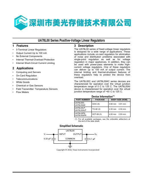
LM78L05
- 格式:pdf
- 大小:377.65 KB
- 文档页数:14
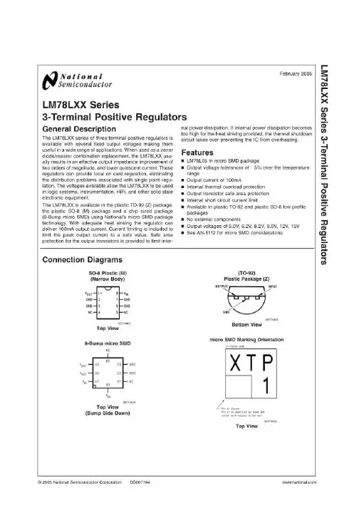
LM78LXX SeriesApril 14, 20113-Terminal Positive RegulatorsGeneral DescriptionThe LM78LXX series of three terminal positive regulators isavailable with several fixed output voltages making them use-ful in a wide range of applications. When used as a zenerdiode/resistor combination replacement, the LM78LXX usu-ally results in an effective output impedance improvement oftwo orders of magnitude, and lower quiescent current. Theseregulators can provide local on card regulation, eliminatingthe distribution problems associated with single point regula-tion. The voltages available allow the LM78LXX to be used inlogic systems, instrumentation, HiFi, and other solid stateelectronic equipment.The LM78LXX is available in the plastic TO-92 (Z) package,the plastic SO-8 (M) package and a chip sized package (8-Bump micro SMD) using National's micro SMD package tech-nology. With adequate heat sinking the regulator can deliver100mA output current. Current limiting is included to limit thepeak output current to a safe value. Safe area protection forthe output transistors is provided to limit internal power dissi-pation. If internal power dissipation becomes too high for theheat sinking provided, the thermal shutdown circuit takes overpreventing the IC from overheating.Features■LM78L05 in micro SMD package■Output voltage tolerances of ±5% over the temperaturerange■Output current of 100mA■Internal thermal overload protection■Output transistor safe area protection■Internal short circuit current limit■Available in plastic TO-92 and plastic SO-8 low profilepackages■No external components■Output voltages of 5.0V, 6.2V, 8.2V, 9.0V, 12V, 15V■See AN-1112 for micro SMD considerations Connection DiagramsSO-8 Plastic (M)(Narrow Body)774402Top View8-Bump micro SMD774424Top View(Bump Side Down)(TO-92)Plastic Package (Z)774403Bottom Viewmicro SMD Marking Orientation774433Top View© 2011 National Semiconductor LM78LXX Series 3-Terminal Positive RegulatorsOrdering InformationPackage NSC Drawing Output VoltageOrder Number Supplied As micro SMD BPA08AAB 5V LM78L05IBPX Reel of 3000Thin micro SMDTPA08AAA5V LM78L05ITP Reel of 250LM78L05ITPX Reel of 30009VLM78L09ITPX Reel of 3000SOIC NarrowM08A5VLM78L05ACMRail of 95LM78L05ACMX Reel of 2500LM78L05AIM Rail of 95LM78L05AIMX Reel of 250012V LM78L12ACMX Reel of 250015V LM78L15ACMX Reel of 2500TO-92Z03A5V LM78L05ACZ Box of 18006.2VLM78L62ACZ Box of 18009V LM78L09ACZ Box of 180012V LM78L12ACZ Box of 180015VLM78L15ACZBox of 1800 2L M 78L X X S e r i e sAbsolute Maximum Ratings (Note 1)If Military/Aerospace specified devices are required,please contact the National Semiconductor Sales Office/Distributors for availability and specifications.Power Dissipation (Note 5)Internally LimitedInput Voltage35VStorage Temperature−65°C to +150°CESD Susceptibility (Note 2)1kVOperating Junction Temperature SO-8, TO-920°C to 125°C SO-8 (5V Only)-40°C to 125°C micro SMD−40°C to 85°C Soldering InformationInfrared or Convection (20 sec.)235°CWave Soldering (10 sec.)260°C (lead time)LM78LXX Electrical CharacteristicsLimits in standard typeface are for T J = 25°C, Bold typeface appliesover the entire operating temperature range of the indicated package. Limits are guaranteed by production testing or correlation techniques using standard Statistical Quality Control (SQC) methods. Unless otherwise specified: I O = 40mA, C I =0.33μF, C O = 0.1μF.LM78L05Unless otherwise specified, V IN = 10V Symbol ParameterConditionsMin Typ Max UnitsV OOutput Voltage4.855.2V7V ≤ V IN ≤ 20V 1mA ≤ I O ≤ 40mA (Note 3)4.755.251mA ≤ I O ≤ 70mA (Note 3)4.755.25ΔV O Line Regulation7V ≤ V IN ≤ 20V 1875mV8V ≤ V IN ≤ 20V1054ΔV O Load Regulation1mA ≤ I O ≤ 100mA 20601mA ≤ I O ≤ 40mA530I Q Quiescent Current35mA ΔI Q Quiescent Current Change8V ≤ V IN ≤ 20V 1.01mA ≤ I O ≤ 40mA0.1V nOutput Noise Voltage f = 10 Hz to 100 kHz (Note 4) 40 μV Ripple Rejectionf = 120 Hz 8V ≤ V IN ≤ 16V 4762 dB I PKPeak Output Current140 mA Average Output Voltage TempcoI O = 5mA −0.65 mV/°C V IN (Min)Minimum Value of Input VoltageRequired to Maintain Line Regulation 6.77V θJAThermal Resistance (8-Bump micro SMD)230.9°C/W LM78LXX SeriesLM78L62ACUnless otherwise specified, V IN = 12V Symbol ParameterConditionsMin Typ Max UnitsV OOutput Voltage5.956.26.45V8.5V ≤ V IN ≤ 20V 1mA ≤ I O ≤ 40mA (Note 3)5.96.51mA ≤ I O ≤ 70mA (Note 3)5.96.5ΔV O Line Regulation8.5V ≤ V IN ≤ 20V 65175mV9V ≤ V IN ≤ 20V55125ΔV O Load Regulation1mA ≤ I O ≤ 100mA 13801mA ≤ I O ≤ 40mA640I Q Quiescent Current 25.5mA ΔI Q Quiescent Current Change8V ≤ V IN ≤ 20V 1.51mA ≤ I O ≤ 40mA0.1V nOutput Noise Voltage f = 10 Hz to 100 kHz (Note 4)50μV Ripple Rejectionf = 120 Hz 10V ≤ V IN ≤ 20V4046dB I PKPeak Output Current140mA Average Output Voltage TempcoI O = 5mA −0.75mV/°C V IN (Min)Minimum Value of Input VoltageRequired to Maintain Line Regulation7.9V LM78L82ACUnless otherwise specified, V IN = 14V Symbol ParameterConditionsMin Typ Max UnitsV OOutput Voltage7.878.28.53V11V ≤ V IN ≤ 23V 1mA ≤ I O ≤ 40mA (Note 3)7.88.61mA ≤ I O ≤ 70mA (Note 3)7.88.6ΔV O Line Regulation11V ≤ V IN ≤ 23V 80175mV12V ≤ V IN ≤ 23V70125ΔV O Load Regulation1mA ≤ I O ≤ 100mA 15801mA ≤ I O ≤ 40mA840I Q Quiescent Current 2 5.5mA ΔI Q Quiescent Current Change12V ≤ V IN ≤ 23V1.51mA ≤ I O ≤ 40mA0.1V nOutput Noise Voltage f = 10 Hz to 100 kHz (Note 4)60μV Ripple Rejectionf = 120 Hz 12V ≤ V IN ≤ 22V3945dB I PKPeak Output Current140mA 4L M 78L X X S e r i e sSymbol ParameterConditionsMin Typ Max Units Average Output Voltage TempcoI O = 5mA−0.8mV/°C V IN (Min)Minimum Value of Input VoltageRequired to Maintain Line Regulation9.9VLM78L09ACUnless otherwise specified, V IN = 15V Symbol ParameterConditionsMin Typ Max UnitsV OOutput Voltage8.649.09.36V11.5V ≤ V IN ≤ 24V 1mA ≤ I O ≤ 40mA (Note 3)8.559.451mA ≤ I O ≤ 70mA (Note 3)8.559.45ΔV O Line Regulation11.5V ≤ V IN ≤ 24V 100200mV13V ≤ V IN ≤ 24V90150ΔV O Load Regulation1mA ≤ I O ≤ 100mA 20901mA ≤ I O ≤ 40mA1045I Q Quiescent Current 25.5mA ΔI Q Quiescent Current Change11.5V ≤ V IN ≤ 24V 1.51mA ≤ I O ≤ 40mA0.1V nOutput Noise Voltage 70μV Ripple Rejectionf = 120 Hz 15V ≤ V IN ≤ 25V3844dB I PKPeak Output Current140mA Average Output Voltage TempcoI O = 5mA −0.9mV/°C V IN (Min)Minimum Value of Input VoltageRequired to Maintain Line Regulation10.7V LM78L12ACUnless otherwise specified, V IN = 19V Symbol ParameterConditionsMin Typ Max UnitsV OOutput Voltage11.51212.5V14.5V ≤ V IN ≤ 27V 1mA ≤ I O ≤ 40mA (Note 3)11.412.61mA ≤ I O ≤ 70mA (Note 3)11.412.6ΔV O Line Regulation14.5V ≤ V IN ≤ 27V 30180mV16V ≤ V IN ≤ 27V20110ΔV O Load Regulation1mA ≤ I O ≤ 100mA 301001mA ≤ I O ≤ 40mA1050I Q Quiescent Current 35mA ΔI Q Quiescent Current Change16V ≤ V IN ≤ 27V 11mA ≤ I O ≤ 40mA0.1V nOutput Noise Voltage80μV LM78LXX SeriesSymbolParameter Conditions Min Typ Max Units Ripple Rejectionf = 120 Hz 15V ≤ V IN ≤ 254054dB I PKPeak Output Current140mA Average Output Voltage TempcoI O = 5mA−1.0mV/°CV IN (Min)Minimum Value of Input VoltageRequired to Maintain Line Regulation13.714.5VLM78L15ACUnless otherwise specified, V IN = 23V Symbol ParameterConditionsMin Typ Max UnitsV OOutput Voltage14.415.015.6V17.5V ≤ V IN ≤ 30V 1mA ≤ I O ≤ 40mA (Note 3)14.2515.751mA ≤ I O ≤ 70mA (Note 3)14.2515.75ΔV O Line Regulation17.5V ≤ V IN ≤ 30V 37250mV20V ≤ V IN ≤ 30V25140ΔV O Load Regulation1mA ≤ I O ≤ 100mA 351501mA ≤ I O ≤ 40mA1275I QQuiescent Current 35mA ΔI QQuiescent Current Change20V ≤ V IN ≤ 30V 11mA ≤ I O ≤ 40mA0.1V nOutput Noise Voltage 90μV Ripple Rejectionf = 120 Hz18.5V ≤ V IN ≤ 28.5V3751dB I PKPeak Output Current140mA Average Output Voltage TempcoI O = 5mA −1.3mV/°C V IN (Min)Minimum Value of Input VoltageRequired to Maintain Line Regulation16.717.5V Note 1:Absolute Maximum Ratings indicate limits beyond which damage to the device may occur. Electrical specifications do not apply when operating the device outside of its stated operating conditions.Note 2:Human body model, 1.5 k Ω in series with 100pF.Note 3:Power dissipation ≤ 0.75W.Note 4:Recommended minimum load capacitance of 0.01μF to limit high frequency noise.Note 5:Typical thermal resistance values for the packages are: Z Package: θJC = 60 °C/W, = θJA = 230 °C/W M Package: θJA = 180 °C/W micro SMD Package: θJA = 230.9°C/W 6L M 78L X X S e r i e sTypical Performance CharacteristicsMaximum Average Power Dissipation (Z Package)774414Peak Output Current774416Dropout Voltage774417Ripple Rejection774418Output Impedance774419Quiescent Current774420LM78LXX SeriesQuiescent Current774421Equivalent CircuitLM78LXX774407 8L M 78L X X S e r i e sTypical ApplicationsFixed Output Regulator774408*Required if the regulator is located more than 3″ from the power supply filter.**See (Note 4) in the electrical characteristics table.Adjustable Output Regulator774409V OUT = 5V + (5V/R1 + I Q ) R25V/R1 > 3 I Q , load regulation (L r ) ≈ [(R1 + R2)/R1] (L r of LM78L05)Current Regulator774410I OUT = (V OUT /R1) + I Q>I Q = 1.5mA over line and load changes5V, 500mA Regulator with Short Circuit Protection774411*Solid tantalum.**Heat sink Q1.***Optional: Improves ripple rejection and transient response.Load Regulation: 0.6% 0 ≤ I L ≤ 250mA pulsed with t ON = 50ms.LM78LXX Series±15V, 100mA Dual Power Supply774412*Solid tantalum.Variable Output Regulator 0.5V-18V774413*Solid tantalum.V OUT = V G + 5V, R1 = (−V IN /I Q LM78L05)V OUT = 5V (R2/R4) for (R2 + R3) = (R4 + R5)A 0.5V output will correspond to (R2/R4) = 0.1 (R3/R4) = 0.9 10L M 78L X X S e r i e sPhysical Dimensions inches (millimeters) unless otherwise notedNOTES: UNLESS OTHERWISE SPECIFIED1. EPOXY COATING2. 63Sn/37Pb EUTECTIC BUMP3. RECOMMEND NON-SOLDER MASK DEFINED LANDING PAD.4. PIN A1 IS ESTABLISHED BY LOWER LEFT CORNER WITH RESPECT TO TEXT ORIENTATION. REMAINING PINS ARE NUMBERED COUNTERCLOCK-WISE.5. XXX IN DRAWING NUMBER REPRESENTS PACKAGE SIZE VARIATION WHERE X1 IS PACKAGE WIDTH, X2IS PACKAGE LENGTH AND X3IS PACKAGEHEIGHT.6. REFERENCE JEDEC REGISTRATION MO-211, VARIATION BC.8-Bump micro SMDNS Package Number BPA08AABX1 = 1.285mm X2 = 1.285mm X3 = 0.850mm LM78LXX Series8-Bump Thin micro SMD NS Package Number TPA08AAAX1 = 1.285mm X2 = 1.285mm X3 = 0.500mmS.O. Package (M)NS Package Number M08A 12L M 78L X X S e r i e sLM78LXX Series Molded Offset TO-92 (Z)NS Package Number Z03ANotesL M 78L X X S e r i e s 3-T e r m i n a l P o s i t i v e R e g u l a t o r sFor more National Semiconductor product information and proven design tools, visit the following Web sites at:ProductsDesign SupportAmplifiers /amplifiers WEBENCH® Tools /webench Audio/audio App Notes /appnotes Clock and Timing /timing Reference Designs /refdesigns Data Converters /adc Samples /samples Interface /interface Eval Boards /evalboards LVDS/lvds Packaging /packaging Power Management /power Green Compliance /quality/green Switching Regulators /switchers Distributors/contacts LDOs /ldo Quality and Reliability /quality LED Lighting /led Feedback/Support /feedback Voltage References /vref Design Made Easy/easy PowerWise® Solutions /powerwiseApplications & Markets /solutions Serial Digital Interface (SDI)/sdiMil/Aero/milaero Temperature Sensors /tempsensors SolarMagic™/solarmagic PLL/VCO/wirelessPowerWise® Design University/trainingTHE CONTENTS OF THIS DOCUMENT ARE PROVIDED IN CONNECTION WITH NATIONAL SEMICONDUCTOR CORPORATION (“NATIONAL”) PRODUCTS. NATIONAL MAKES NO REPRESENTATIONS OR WARRANTIES WITH RESPECT TO THE ACCURACY OR COMPLETENESS OF THE CONTENTS OF THIS PUBLICATION AND RESERVES THE RIG HT TO MAKE CHANG ES TO SPECIFICATIONS AND PRODUCT DESCRIPTIONS AT ANY TIME WITHOUT NOTICE. NO LICENSE, WHETHER EXPRESS,IMPLIED, ARISING BY ESTOPPEL OR OTHERWISE, TO ANY INTELLECTUAL PROPERTY RIG HTS IS G RANTED BY THIS DOCUMENT.TESTING AND OTHER QUALITY CONTROLS ARE USED TO THE EXTENT NATIONAL DEEMS NECESSARY TO SUPPORT NATIONAL’S PRODUCT WARRANTY. EXCEPT WHERE MANDATED BY G OVERNMENT REQUIREMENTS, TESTING OF ALL PARAMETERS OF EACH PRODUCT IS NOT NECESSARILY PERFORMED. NATIONAL ASSUMES NO LIABILITY FOR APPLICATIONS ASSISTANCE OR BUYER PRODUCT DESIG N. BUYERS ARE RESPONSIBLE FOR THEIR PRODUCTS AND APPLICATIONS USING NATIONAL COMPONENTS. PRIOR TO USING OR DISTRIBUTING ANY PRODUCTS THAT INCLUDE NATIONAL COMPONENTS, BUYERS SHOULD PROVIDE ADEQUATE DESIGN, TESTING AND OPERATING SAFEGUARDS.EXCEPT AS PROVIDED IN NATIONAL’S TERMS AND CONDITIONS OF SALE FOR SUCH PRODUCTS, NATIONAL ASSUMES NO LIABILITY WHATSOEVER, AND NATIONAL DISCLAIMS ANY EXPRESS OR IMPLIED WARRANTY RELATING TO THE SALE AND/OR USE OF NATIONAL PRODUCTS INCLUDING LIABILITY OR WARRANTIES RELATING TO FITNESS FOR A PARTICULAR PURPOSE, MERCHANTABILITY, OR INFRING EMENT OF ANY PATENT, COPYRIG HT OR OTHER INTELLECTUAL PROPERTY RIGHT.LIFE SUPPORT POLICYN ATION AL’S PRODUCTS ARE N OT AUTHORIZED FOR USE AS CRITICAL COMPON EN TS IN LIFE SUPPORT DEVICES OR SYSTEMS WITHOUT THE EXPRESS PRIOR WRITTEN APPROVAL OF THE CHIEF EXECUTIVE OFFICER AN D GEN ERAL COUNSEL OF NATIONAL SEMICONDUCTOR CORPORATION. As used herein:Life support devices or systems are devices which (a) are intended for surgical implant into the body, or (b) support or sustain life and whose failure to perform when properly used in accordance with instructions for use provided in the labeling can be reasonably expected to result in a significant injury to the user. A critical component is any component in a life support device or system whose failure to perform can be reasonably expected to cause the failure of the life support device or system or to affect its safety or effectiveness.National Semiconductor and the National Semiconductor logo are registered trademarks of National Semiconductor Corporation. All other brand or product names may be trademarks or registered trademarks of their respective holders.Copyright© 2011 National Semiconductor CorporationFor the most current product information visit us at National Semiconductor Americas Technical Support CenterEmail: support@ Tel: 1-800-272-9959National Semiconductor Europe Technical Support CenterEmail: europe.support@National Semiconductor Asia Pacific Technical Support Center Email: ap.support@National Semiconductor Japan Technical Support Center Email: jpn.feedback@。