
L78MS05J中文资料
- 格式:pdf
- 大小:533.43 KB
- 文档页数:6
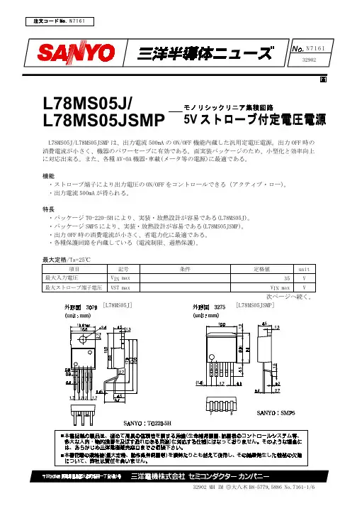
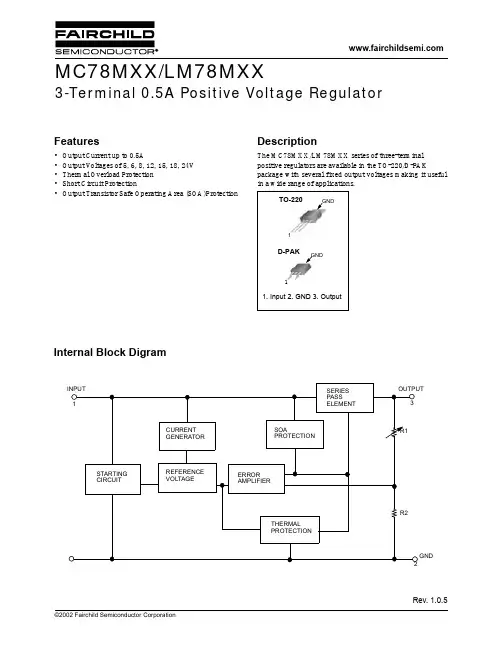
Rev. 1.0.5Features•Output Current up to 0.5A•Output V oltages of 5, 6, 8, 12, 15, 18, 24V •Thermal Overload Protection •Short Circuit Protection•Output Transistor Safe Operating Area (SOA)ProtectionDescriptionThe MC78MXX/LM78MXX series of three-terminal positive regulators are available in the TO-220/D-PAKpackage with several fixed output voltages making it useful in a wide range of applications.TO-220D-PAK1. Input2. GND3. Output11GNDGNDInternal Block DigramOUTPUT3R1R2GND 21INPUT SERIES PASSELEMENTSOAPROTECTIONCURRENT GENERATOR STARTING CIRCUITREFERENCE VOLTAGEERROR AMPLIFIERTHERMAL PROTECTIONMC78MXX/LM78MXX3-Terminal 0.5A Positive Voltage RegulatorMC78MXX/LM78MXXAbsolute Maximum RatingsNote:1. Thermal resistance test boardSize: 76.2mm * 114.3mm * 1.6mm(1S0P)JEDEC standard: JESD51-3, JESD51-72. Assume no ambient airflowElectrical Characteristics (MC78M05/LM78M05)(Refer to the test circuits, 0 < T J < +125°C, I O =350mA, V I =10V, unless otherwise specified, C I = 0.33µF, C O =0.1µF)Note:3. Load and line regulation are specified at constant junction temperature. Change in V o due to heating effects must be takeninto account separately. Pulse testing with low duty is used.ParameterSymbol Value Unit Input Voltage (for V O = 5V to 18V)(for V O = 24V)V I V I 3540V V Thermal Resistance Junction-Case (Note1)TO-220 (Tc = +25°C)R θJC 2.5°C/W Thermal Resistance Junction-Air (Note1, 2)TO-220 (Ta = +25°C)D-PAK (Ta = +25°C)R θJA 6692°C/W Operating Junction Temperature Range T OPR 0 ~ +150°C Storage Temperature RangeT STG-65 ~ +150°CParameter Symbol ConditionsMin.Typ.Max.UnitOutput VoltageV OT J = +25°C 4.85 5.2V I O = 5mA to 350mA V I = 7V to 20V 4.755 5.25Line Regulation (Note3)∆V O I O = 200mA T J =+25°CV I = 7V to 25V --100mV V I = 8V to 25V--50Load Regulation (Note3)∆V O I O = 5mA to 0.5A, T J =+25°C --100mV I O = 5mA to 200mA, T J =+25 °C --50Quiescent Current I Q T J =+25°C- 4.0 6.0mAQuiescent Current Change∆I Q I O = 5mA to 350mA --0.5mA I O = 200mA V I = 8V to 25V --0.8Output Voltage Drift ∆V/∆T I O = 5mAT J = 0 to +125°C --0.5-mV/°COutput Noise Voltage V N f = 10Hz to 100kHz -40-µV/VoRipple Rejection RR f = 120Hz, I O = 300mA V I = 8V to 18V, T J =+25 °C -80-dB Dropout Voltage V D T J =+25°C, I O = 500mA -2-V Short Circuit Current I SC T J =+25°C, V I = 35V -300-mA Peak CurrentI PKT J =+25°C-700-mAMC78MXX/LM78MXXElectrical Characteristics (MC78M06) (Continued)(Refer to the test circuits, 0 < T J < +125°C, I O =350mA, V I =11V, unless otherwise specified, C I =0.33µF, C O =0.1µF)Note:1. Load and line regulation are specified at constant junction temperature. Change in V o due to heating effects must be takeninto account separately. Pulse testing with low duty is used.Parameter Symbol ConditionsMin.Typ.Max.UnitOutput VoltageV OT J = +25°C 5.756 6.25V I O = 5mA to 350mA V I = 8V to 21V 5.76 6.3Line Regulation (Note1)∆V O I O = 200mA T J = +25°CV I = 8V to 25V --100mV V I = 9V to 25V--50Load Regulation (Note1)∆V O I O = 5mA to 0.5A, T J = +25°C --120mV I O = 5mA to 200mA, T J = +25°C --60Quiescent Current I Q T J = +25°C - 4.0 6.0mAQuiescent Current Change∆I Q I O = 5mA to 350mA --0.5mA I O = 200mA V I = 9V to 25V --0.8Output Voltage Drift ∆V/∆T I O = 5mAT J = 0 to +125°C --0.5-mV/°COutput Noise Voltage V N f = 10Hz to 100kHz -45-µV/VoRipple Rejection RR f = 120Hz, I O = 300mA V I = 9V to 19V, T J =+25 °C -80-dB Dropout Voltage V D T J =+25°C, I O = 500mA -2-V Short Circuit Current I SC T J = +25°C, V I = 35V -300-mA Peak CurrentI PKT J =+25°C-700-mAMC78MXX/LM78MXXElectrical Characteristics (MC78M08) (Continued)(Refer to the test circuits, 0 < T J < +125°C, I O =350mA, V I =14V, unless otherwise specified, C I = 0.33µF, C O =0.1µF)Note:1. Load and line regulation are specified at constant junction temperature. Change in V O due to heating effects must be takeninto account separately. Pulse testing with low duty is used.Parameter SymbolConditionsMin.Typ.Max.UnitOutput VoltageV OT J =+25°C7.788.3V I O = 5mA to 350mA V I = 10.5V to 23V 7.688.4Line Regulation (Note1)∆V O I O = 200mA T J =+25°CV I = 10.5V to 25V --100mV V I = 11V to 25V --50Load Regulation (Note1)∆V O I O = 5mA to 0.5A, T J =+25°C --160mV I O = 5mA to 200mA, T J =+25°C --80Quiescent Current I Q T J = +25°C - 4.0 6.0mAQuiescent Current Change∆I Q I O = 5mA to 350mA --0.5mA I O = 200mAV I = 10.5V to 25V --0.8Output Voltage Drift RR I O = 5mAT J = 0 to +125°C -−0.5-mV/°COutput Noise Voltage V N f = 10Hz to 100kHz-52-µV/VoRipple Rejection RR f = 120Hz, I O = 300mAV I = 11.5V to 21.5V, T J =+25 °C -80-dB Dropout Voltage V D T J = +25°C, I O = 500mA -2-V Short Circuit Current I SC T J = +25°C, V I = 35V -300-mA Peak CurrentI PKT J = +25°C-700-mA(Refer to the test circuits, 0 < T J < +125°C, I O =350mA, V I =19V, unless otherwise specified, C I =0.33µF, C O =0.1µF)Note:1. Load and line regulation are specified at constant junction temperature. Change in V o due to heating effects must be takeninto account separately. Pulse testing with low duty is used.Parameter SymbolConditionsMin.Typ.Max.UnitOutput VoltageV OT J = +25°C11.51212.5V I O = 5mA to 350mA V I = 14.5V to 27V 11.41212.6Line Regulation (Note1)∆V O I O = 200mA T J = +25°CV I = 14.5V to 30V --100mV V I = 16V to 30V --50Load Regulation (Note1)∆V O I O = 5mA to 0.5A, T J = +25°C --240mV I O = 5mA to 200mA, T J = +25°C --120Quiescent Current I Q T J =+25°C- 4.1 6.0mAQuiescent Current Change∆I Q I O = 5mA to 350mA --0.5mA I O = 200mAV I = 14.5V to 30V --0.8Output Voltage Drift ∆V/∆T I O = 5mAT J = 0 to +125°C --0.5-mV/°COutput Noise Voltage V N f = 10Hz to 100kHz-75-µV/VoRipple Rejection RR f = 120Hz, I O = 300mAV I = 15V to 25V, T J =+25 °C -80-dB Dropout Voltage V D T J =+25°C, I O = 500mA -2-V Short Circuit Current I SC T J = +25°C, V I = 35V -300-mA Peak CurrentI PKT J = +25°C-700-mA(Refer to the test circuits, 0 < T J < +125°C, I O =350mA, V I =23V, unless otherwise specified, C I =0.33µF, C O =0.1µF)Note:1. Load and line regulation are specified at constant junction temperature. Change in V O due to heating effects must be takeninto account separately. Pulse testing with low duty is used.Parameter Symbol ConditionsMin.Typ.Max.UnitOutput VoltageV OT J = +25°C 14.41515.6V I O = 5mA to 350mA V I = 17.5V to 30V 14.251515.75Line Regulation (Note1)∆V O I O = 200mA T J =+25°CV I = 17.5V to 30V --100mV V I = 20V to 30V--50Load Regulation (Note1)∆V O I O = 5mA to 0.5A, T J =+25°C --300mV I O = 5mA to 200mA, T J =+25°C --150Quiescent Current I Q T J = +25°C - 4.1 6.0mAQuiescent Current Change∆I Q I O = 5mA to 350mA --0.5mA I O = 200mAV I = 17.5V to 30V --0.8Output Voltage Drift ∆V/∆T I O = 5mAT J = 0 to +125°C --1-mV/°COutput Noise Voltage V N f = 10Hz to 100kHz-100-µV/VoRipple Rejection RR f = 120Hz, I O = 300mAV I = 18.5V to 28.5V, T J =+25 °C -70-dB Dropout Voltage V D T J =+25°C, I O = 500mA -2-V Short Circuit Current I SC T J = +25°C, V I = 35V -300-mA Peak CurrentI PKT J = +25°C-700-mAMC78MXX/LM78MXXElectrical Characteristics (MC78M18) (Continued)(Refer to the test circuits, 0 < T J < +125°C, I O =350mA, V I =26V, unless otherwise specified, C I =0.33µF, C O =0.1µF)Note:1. Load and line regulation are specified at constant junction temperature. Change in V O due to heating effects must be takeninto account separately. Pulse testing with low duty is used.Parameter SymbolConditionsMin.Typ.Max.UnitOutput VoltageV OT J = +25°C17.31818.7V I O = 5mA to 350mA V I = 20.5V to 33V 17.11818.9Line Regulation (Note1)∆V O I O = 200mA T J = +25°CV I = 21V to 33V --100mV V I = 24V to 33V --50Load Regulation (Note1)∆V ΟI O = 5mA to 0.5A, T J = +25°C --360mV I O = 5mA to 200mA, T J = +25°C --180Quiescent Current I Q T J = +25°C - 4.2 6.0mAQuiescent Current Change ∆I Q I O = 5mA to 350mA --0.5mA I O = 200mA V I = 21V to 33V--0.8Output Voltage Drift ∆V/∆T I O = 5mAT J = 0 to 125°C --1.1-mV/°C Output Noise Voltage V N f = 10Hz to 100kHz-100-µV/Vo Ripple Rejection RR f = 120Hz, I O = 300mA , V I = 22V to 32V T J =+25 °C-70-dB Dropout Voltage V D T J = +25°C, I O = 500mA -2-V Short Circuit Current I SC T J = +25°C, V I = 35V -300-mA Peak CurrentI PKT J = +25°C-700-mAElectrical Characteristics (MC78M24) (Continued)(Refer to the test circuits, 0 < T J < +125°C, I O =350mA, V I =33V, unless otherwise specified, C I =0.33µF, C O =0.1µF)Note:1. Load and line regulation are specified at constant junction temperature. Change in V O due to heating effects must be takeninto account separately. Pulse testing with low duty is used.Parameter Symbol ConditionsMin.Typ.Max.UnitOutput VoltageV OT J =+25°C 232425V I O = 5mA to 350mA V I = 27V to 38V22.82425.2Line Regulation (Note1)∆V O I O = 200mA T J =+25°C V I = 27V to 38V --100mV V I = 28V to 38V --50Load Regulation (Note1)∆V O I O = 5mA to 0.5A, T J =+25°C --480mV I O = 5mA to 200mA, T J =+25°C --240Quiescent CurrentI QT J = +25°C - 4.2 6.0mAQuiescent Current Change∆I Q I O = 5mA to 350mA--0.5mA I O = 200mA V I = 27V to 38V --0.8Output Voltage Drift ∆V/∆T I O = 5mAT J = 0 to +125°C --1.2-mV/°COutput Noise Voltage V N f = 10Hz to 100kHz-170-µV/VoRipple Rejection RR f = 120Hz, I O = 300mAV I = 28V to 38V, T J =+25 °C -70-dB Dropout Voltage V D T J = +25°C, I O = 500mA -2-V Short Circuit Current I SC T J = +25°C, V I = 35V -300-mA Peak CurrentI PKT J = +25°C-700-mATypical ApplicationsFigure 1.Fixed Output RegulatorFigure 2.Constant Current RegulatorNotes:1.To specify an output voltage, substitute voltage value for "XX"2.Although no output capacitor is needed for stability, it does improve transient response.3.C I is required if regulator is located an appreciable distance from power Supply filterFigure 3.Circuit for Increasing Output Voltage0.1µFC OC I0.3µFV OV IMC78MXX LM78MXX1320.1µFC OC I0.33µFI OV IMC78MXX LM78MXX132VXXI O R 1I O = R 1 +I OVxx 0.1µFC OC I0.33µFI OV IMC78MXX LM78MXX132V XXV OR 1R 2I R1 ≥ 5I OV O = V XX (1+R 2/R 1) +I O R 2MC78MXX/LM78MXXFigure 4.Adjustable Output Regulator (7 to 30V)Figure 5.0.5 to 10V Regulator0.1µFC OC I0.33µFV OV IMC78M05LM78M0513210k Ω32476LM7410.1µFC2C10.33µFV OV IMC78M05LM78M0513210k Ω32476LM741R3R1VXXR4R5910Ω9.1k Ω13V < V I < 25V-7 < -VI < 17V_+VO = VxxR 1R 4Mechanical DimensionsPackageDimensions in millimetersTO-22011Mechanical Dimensions (Continued)PackageDimensions in millimetersD-PAK1213Ordering InformationProduct Number Package Operating TemperatureLM78M05CT TO-2200 ~ +125°C Product Number PackageOperating TemperatureMC78M05CT TO-2200 ~ +125°CMC78M06CT MC78M08CT MC78M12CT MC78M15CT MC78M18CT MC78M24CT MC78M05CDT D-PAKMC78M06CDT MC78M08CDT MC78M12CDT11/12/02 0.0m 001Stock#DSxxxxxxxx2002 Fairchild Semiconductor CorporationLIFE SUPPORT POLICYFAIRCHILD’S PRODUCTS ARE NOT AUTHORIZED FOR USE AS CRITICAL COMPONENTS IN LIFE SUPPORT DEVICES OR SYSTEMS WITHOUT THE EXPRESS WRITTEN APPROVAL OF THE PRESIDENT OF FAIRCHILD SEMICONDUCTOR CORPORATION. As used herein:1.Life support devices or systems are devices or systemswhich, (a) are intended for surgical implant into the body, or (b) support or sustain life, and (c) whose failure to perform when properly used in accordance with instructions for use provided in the labeling, can bereasonably expected to result in a significant injury of the user.2. A critical component in any component of a life supportdevice or system whose failure to perform can bereasonably expected to cause the failure of the life support device or system, or to affect its safety or effectiveness.DISCLAIMERFAIRCHILD SEMICONDUCTOR RESERVES THE RIGHT TO MAKE CHANGES WITHOUT FURTHER NOTICE TO ANY PRODUCTS HEREIN TO IMPROVE RELIABILITY, FUNCTION OR DESIGN. FAIRCHILD DOES NOT ASSUME ANYLIABILITY ARISING OUT OF THE APPLICATION OR USE OF ANY PRODUCT OR CIRCUIT DESCRIBED HEREIN; NEITHER DOES IT CONVEY ANY LICENSE UNDER ITS PATENT RIGHTS, NOR THE RIGHTS OF OTHERS.。

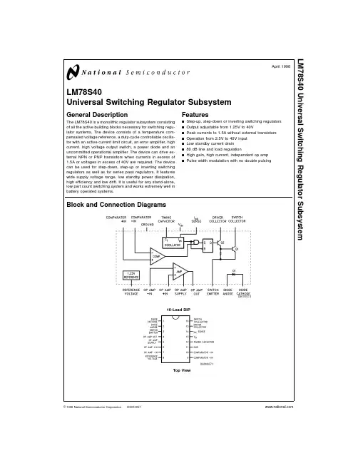
LM78S40Universal Switching Regulator SubsystemGeneral DescriptionThe LM78S40is a monolithic regulator subsystem consisting of all the active building blocks necessary for switching regu-lator systems.The device consists of a temperature com-pensated voltage reference,a duty-cycle controllable oscilla-tor with an active current limit circuit,an error amplifier,high current,high voltage output switch,a power diode and an uncommitted operational amplifier.The device can drive ex-ternal NPN or PNP transistors when currents in excess of 1.5A or voltages in excess of 40V are required.The device can be used for step-down,step-up or inverting switching regulators as well as for series pass regulators.It features wide supply voltage range,low standby power dissipation,high efficiency and low drift.It is useful for any stand-alone,low part count switching system and works extremely well in battery operated systems.Featuresn Step-up,step-down or inverting switching regulators n Output adjustable from 1.25V to 40Vn Peak currents to 1.5A without external transistors n Operation from 2.5V to 40V input n Low standby current drain n 80dB line and load regulationn High gain,high current,independent op amp nPulse width modulation with no double pulsingBlock and Connection DiagramsDS010057-216-Lead DIPDS010057-1Top ViewApril 1998LM78S40Universal Switching Regulator Subsystem©1998National Semiconductor Corporation Ordering InformationPart Number NS Package Temperature Range LM78S40J/883J16A Ceramic DIP−55˚C to+125˚C LM78S40N N16E Molded DIP−40˚C to+125˚C LM78S40CN N16E Molded DIP0˚C to+70˚C2Absolute Maximum Ratings(Note1)If Military/Aerospace specified devices are required, please contact the National Semiconductor Sales Office/ Distributors for availability and specifications.Storage Temperature RangeCeramic DIP−65˚C to+175˚C Molded DIP−65˚C to+150˚C Operating Temperature RangeExtended(LM78S40J)−55˚C to+125˚C Industrial(LM78S40N)−40˚C to+125˚C Commercial(LM78S40CN)0˚C to+70˚C Lead TemperatureCeramic DIP(Soldering,60sec.)300˚C Molded DIP(Soldering,10sec.)265˚C Internal Power Dissipation(Note2)(Note3)16L-Ceramic DIP 1.50W 16L-Molded DIP 1.04W Input Voltage from V IN to GND40V Input Voltage from V+(Op Amp)to GND40V Common Mode Input Range(Comparator and Op Amp)−0.3to V+ Differential Input Voltage(Note4)±30V Output Short CircuitDuration(Op Amp)Continuous Current from V REF10mA Voltage from SwitchCollectors to GND40V Voltage from SwitchEmitters to GND40V Voltage from SwitchCollectors to Emitter40V Voltage from Power Diode to GND40V Reverse Power Diode Voltage40V Current through Power Switch 1.5A Current through Power Diode 1.5A ESD Susceptibility(to be determined)LM78S40Electrical Characteristics(Note5)T A=Operating temperature range,V IN=5.0V,V+(Op Amp)=5.0V,unless otherwise specified.Symbol Parameter Conditions Min Typ Max Units GENERAL CHARACTERISTICSI CC Supply Current V IN=5.0V 1.8 3.5mA(Op Amp Disconnected)V IN=40V 2.3 5.0mAI CC Supply Current V IN=5.0V 4.0mA(Op Amp Connected)V IN=40V 5.5mA REFERENCE SECTIONV REF Reference Voltage I REF=1.0mA Extend−55˚C<T A<+125˚C,Comm0<T A<+70˚C, 1.180 1.245 1.310VIndus−40˚C<T A<+85˚CV R LINE Reference Voltage V IN=3.0V to V IN=40V,0.040.2mV/V Line Regulation I REF=1.0mA,T A=25˚CV R LOAD Reference Voltage I REF=1.0mA to I REF=10mA,0.20.5mV/mA Load Regulation T A=25˚COSCILLATOR SECTIONI CHG Charging Current V IN=5.0V,T A=25˚C2050µAI CHG Charging Current V IN=40V,T A=25˚C2070µAI DISCHG Discharge Current V IN=5.0V,T A=25˚C150250µAI DISCHG Discharge Current V IN=40V,T A=25˚C150350µAV OSC Oscillator Voltage Swing V IN=5.0V,T A=25˚C0.5Vt on/t off Ratio of Charge/ 6.0µs/µs Discharge TimeCURRENT LIMIT SECTIONV CLS Current Limit SenseVoltageT A=25˚C250350mV OUTPUT SWITCH SECTIONV SAT1Output Saturation Voltage1I SW=1.0A(Figure1) 1.1 1.3VV SAT2Output Saturation Voltage2I SW=1.0A(Figure2)0.450.7VLM78S40Electrical Characteristics(Note5)(Continued)T A=Operating temperature range,V IN=5.0V,V+(Op Amp)=5.0V,unless otherwise specified.Symbol Parameter Conditions Min Typ Max Units OUTPUT SWITCH SECTIONh FE Output Transistor CurrentI C=1.0A,V CE=5.0V,T A=25˚C70GainI L Output Leakage Current V O=40V,T A=25˚C10nA POWER DIODEV FD Forward Voltage Drop I D=1.0A 1.25 1.5V I DR Diode Leakage Current V D=40V,T A=25˚C10nA COMPARATORV IO Input Offset Voltage V CM=V REF 1.515mV I IB Input Bias Current V CM=V REF35200nA I IO Input Offset Current V CM=V REF 5.075nA V CM Common Mode VoltageT A=25˚C0V IN–2V RangeV IN=3.0V to40V,T A=25˚C7096dB PSRR Power Supply RejectionRatioOPERATIONAL AMPLIFIERV IO Input Offset Voltage V CM=2.5V 4.015mV I IB Input Bias Current V CM=2.5V30200nA I IO Input Offset Current V CM=2.5V 5.075nA A VS+Voltage Gain+R L=2.0kΩto GND;25250V/mVV O=1.0V to2.5V,T A=25˚CA VS−Voltage Gain−R L=2.0kΩto V+(Op Amp)25250V/mVV O=1.0V to2.5V,T A=25˚CV CM Common Mode VoltageT A=25˚C0V CC−2V RangeCMR Common Mode Rejection V CM=0V to3.0V,T A=25˚C76100dB PSRR Power Supply RejectionV+(Op Amp)=3.0V to40V,T A=25˚C76100dB RatioI O+Output Source Current T A=25˚C75150mA I O−Output Sink Current T A=25˚C1035mA SR Slew Rate T A=25˚C0.6V/µs V OL Output Voltage LOW I L=−5.0mA,T A=25˚C 1.0V V OH Output Voltage High I L=50mA,T A=25˚C V+(Op VAmp)−3VNote1:Absolute Maximum Ratings indicate limits beyond which damage to the device may occur.Electrical specifications do not apply when ordering the device beyond its rated operating conditions.Note2:T J Max=150˚C for the Molded DIP,and175˚C for the Ceramic DIP.Note3:Ratings apply to ambient temperature at25˚C.Above this temperature,derate the16L-Ceramic DIP at10mW/˚C,and the16L-Molded DIP at8.3mW/˚C.Note4:For supply voltages less than30V,the absolute maximum voltage is equal to the supply voltage.Note5:A military RETS specification is available on request.At the time of printing,the LM78S40RETS specification complied with the Min and Max limits in this table.The LM78S40J may also be procured as a Standard Military Drawing.4Typical Performance CharacteristicsDesign FormulasCharacteristic Step-Down Step-Up Inverting UnitsFunctional DescriptionSWITCHING FREQUENCY CONTROLThe LM78S40is a variable frequency,variable duty cycle device.The initial switching frequency is set by the timing capacitor.(Oscillator frequency is set by a single external capacitor and may be varied over a range of100Hz to 100kHz).The initial duty cycle is6:1.This switching fre-quency and duty cycle can be modified by two mechanisms—the current limit circuitry(I pk sense)and the comparator.The comparator modifies the OFF time.When the output voltage is correct,the comparator output is in the HIGH state and has no effect on the circuit operation.If the out-put voltage is too high then the comparator output goes LOW.In the LOW state the comparator inhibits the turn-on of the output stage switching transistors.As long as the comparator is LOW the system is in OFF time.As the out-put current rises the OFF time decreases.As the output current nears its maximum the OFF time approaches its minimum value.The comparator can inhibit several ON cycles,one ON cycle or any portion of an ON cycle.Once the ON cycle has begun the comparator cannot inhibit un-til the beginning of the next ON cycle.The current limit modifies the ON time.The current limit is activated when a300mV potential appears between lead 13(V CC)and lead14(I pk).This potential is intended to re-sult when designed for peak current flows through R SC. When the peak current is reached the current limit is turned on.The current limit circuitry provides for a quick end to ON time and the immediate start of OFF time. Generally the oscillator is free running but the current limit action tends to reset the timing cycle.Increasing load results in more current limited ON time and less OFF time.The switching frequency increases with load current.USING THE INTERNAL REFERENCE,DIODE,AND SWITCHThe internal1.245V reference(pin8)must be bypassed, with0.1µF directly to the ground pin(pin11)of the LM78S40,to assure its stability.V FD is the forward voltage drop across the internal power diode.It is listed on the data sheet as1.25V typical,1.5V maximum.If an external diode is used,then its own for-ward voltage drop must be used for V FD.V SAT is the voltage across the switch element(output tran-sistors Q1and Q2)when the switch is closed or ON.This is listed on the data sheet as Output Saturation Voltage.“Output saturation voltage1”is defined as the switching element voltage for Q2and Q1in the Darlington configu-ration with collectors tied together.This applies to Figure 1,the step down mode.“Output saturation voltage2”is the switching element volt-age for Q1only when used as a transistor switch.This ap-plies to Figure2,the step up mode.For the inverting mode,Figure3,the saturation voltage of the external transistor should be used for V SAT.Typical ApplicationsCharacteristic Condition TypicalValue Output Voltage I O=200mA10V Line Regulation20V≤V I≤30V 1.5mV Load Regulation 5.0mA≤I O 3.0mVI O≤300mAMax Output Current V O=9.5V500mA Output Ripple I O=200mA50mV Efficiency I O=200mA74% Standby Current I O=200mA 2.8mA Note7:For I O≥200mA use external diode to limit on-chip power dissipation.DS010057-3 FIGURE1.Typical Step-Down Regulator andOperational Performance(T A=25˚C)6Typical Applications(Continued)Characteristic Condition TypicalValue Output Voltage I O=50mA25V Line Regulation 5.0V≤V I≤15V 4.0mV Load Regulation 5.0mA≤I O 2.0mVI O≤100mAMax Output Current V O=23.75V160mA Output Ripple I O=50mA30mV Efficiency I O=50mA79% Standby Current I O=50mA 2.6mACharacteristic Condition TypicalValue Output Voltage I O=100mA−15V Line Regulation8.0V≤V I≤18V 5.0mV Load Regulation 5.0mA≤I O 3.0mVI O≤150mAMax Output Current V O=14.25V160mA Output Ripple I O=100mA20mV Efficiency I O=100mA70% Standby Current I O=100mA 2.3mADS010057-4FIGURE2.Typical Step-Up Regulator and Operational Performance(T A=25˚C)DS010057-5FIGURE3.Typical Inverting Regulator andOperational Performance(T A=25˚C)Typical Applications(Continued)DS010057-10 FIGURE4.Pulse Width Modulated Step-Down Regulator(f OSC=20kHz)8Physical Dimensions inches(millimeters)unless otherwise noted16-Lead Ceramic Dual-In-Line Package(J)Order Number LM78S40J/883NS Package Number J16A16-Lead Molded Dual-In-Line Package(N)Order Number LM78S40N or LM78S40CNNS Package Number N16ALIFE SUPPORT POLICYNATIONAL’S PRODUCTS ARE NOT AUTHORIZED FOR USE AS CRITICAL COMPONENTS IN LIFE SUPPORT DE-VICES OR SYSTEMS WITHOUT THE EXPRESS WRITTEN APPROVAL OF THE PRESIDENT OF NATIONAL SEMI-CONDUCTOR CORPORATION.As used herein:1.Life support devices or systems are devices or sys-tems which,(a)are intended for surgical implant intothe body,or (b)support or sustain life,and whose fail-ure to perform when properly used in accordancewith instructions for use provided in the labeling,can be reasonably expected to result in a significant injury to the user.2.A critical component in any component of a life support device or system whose failure to perform can be rea-sonably expected to cause the failure of the life support device or system,or to affect its safety or effectiveness.National Semiconductor Corporation AmericasTel:1-800-272-9959Fax:1-800-737-7018Email:support@National Semiconductor EuropeFax:+49(0)180-5308586Email:europe.support@Deutsch Tel:+49(0)180-5308585English Tel:+49(0)180-5327832Français Tel:+49(0)180-5329358Italiano Tel:+49(0)180-5341680National Semiconductor Asia Pacific Customer Response Group Tel:65-2544466Fax:65-2504466Email:sea.support@National Semiconductor Japan Ltd.Tel:81-3-5620-6175Fax:81-3-5620-6179L M 78S 40U n i v e r s a l S w i t c h i n g R e g u l a t o r S u b s y s t e mNational does not assume any responsibility for use of any circuitry described,no circuit patent licenses are implied and National reserves the right at any time without notice to change said circuitry and specifications.。
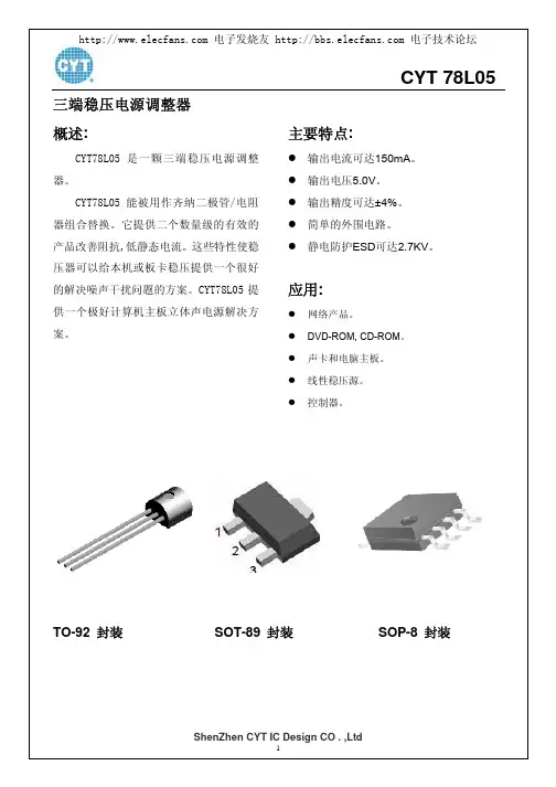
TO-92 SOT-891. VOUT2. GND3. GND4. NC5. NC6. GND7. GND8.VINSOP-8CYT78L05GND10uF 10uF最大的额定值:参数符号 额定值 单位功耗 P 0.75 W 输入电压 V IN 18V 封装热阻抗 ӨJA 150(TO-92) ℃/W 烙铁焊接温度 (10秒) T LEAD 260℃ 工作温度范围 T J 0 to +125 ℃ 存储温度 T STG-65 to +150℃静电防护V ESD 2.7KV电性能参数:VIN = 10V; IOUT = 10mA; CIN = 0.33µF; COUT = 0.1µF TJ = 25°C; 有特殊说明的除外。
符号参数测试条件最小值典型值最大值单位V OUT 输出电压4.8 55.2 V△V OUT /V OUT 空载调整率 7V ≤ V IN ≤ 18V -- 11 45 △V OUT /V OUT负载调整率(5) 1mA ≤ I OUT ≤ 100mA -- 5 50 mVI Q 静态电流 -- 4.3 68V ≤ V IN ≤ 18V -- 1.1 -- △I Q 静态电流调整率 1mA ≤ I OUT ≤ 40mA--0.13--mA△V IN /V OUT输出纹波抑制 F=120Hz , 8V ≤ V IN ≤16V -- 62 -- dB I PK 最大输出电流 -- 150 -- mA△V OUT /△T 输出电压温度系数 I OUT =5mA --0.66 -- MV/℃V IN (Min) 空载最小输入电压-- 6.1 6.4 V静态电流与输入电压静态电流嗻mA 嗼输入电压(V ) 结温(℃) 静态电流嗻mA 嗼静态电流与结温压差与结温压差嗻V 嗼结温(℃) 压差:△V OUT =2%压差与输出电流压差嗻V 嗼输出电流(mA )纹波抑制纹波抑制嗻dB 嗼封装尺寸图: TO-92封装尺寸图: SOP-8尺寸英制(in ) 公制(mm) 编号 最小 最大最小 最大A 0.175 0.205 4.445 5.207B 0.170 0.210 4.318 5.334 E 0.500 0.610 12.70 15.50 F 0.016 0.021 0.407 0.533 G 0.045 0.055 1.143 1.397 H 0.095 0.105 2.413 2.667 J 0.080 0.105 2.032 2.667 K0.125 0.165 3.175 4.191尺寸英制(in ) 公制(mm) 编号 最小 最大最小 最大A 0.05320.0688 0.35 1.75 A1 0.00400.0098 0.10 0.25B 0.01300.0200 0.33 0.51 B1 0.050BSC 1.27BSCC 0.00750.0098 0.19 0.25D 0.18900.1968 4.80 5.00 H 0.22840.2440 5.80 6.20 E0.14970.1574 3.80 4.00封装尺寸图: SOT-89英制(in)公制(mm)编号最小最大最小最大A 0.173 0.181 4.400 4.600B 0.159 0.167 4.050 4.250C 0.067 0.075 1.700 1.900D 0.051 0.059 1.300 1.500E 0.094 0.102 2.400 2.600F 0.035 0.047 0.890 1.200G 0.118REF 3.00REFH 0.059REF 1.50REFI 0.016 0.020 0.400 0.520J 0.055 0.063 1.400 1.600K 0.014 0.016 0.350 0.410L 10°TYP 10°TYPM 0.028REF 0.70REF。