MAX1647电源管理电路设计详解
- 格式:docx
- 大小:11.29 KB
- 文档页数:2

电源管理电路设计随着电子技术的飞速发展,电子产品在人们的日常生活中越来越普及。
电子产品绝大部分都需要电源来供电,并且电源管理电路的设计关系到电子产品的性能和稳定性。
本文将分别从电源管理电路的基本要求、设计流程、以及常见设计问题三个方面进行探讨。
一、电源管理电路的基本要求电源管理电路的基本要求包括以下几个方面:1、稳定性:电源管理电路要保证输出电压、电流的稳定性,防止因为电压波动而出现故障。
2、高效性:电源管理电路要充分利用能量,达到预期的功率转换效率。
3、绿色环保:电源管理电路要遵循环保要求,尽量达到低能耗、低噪声、低辐射的目的,减少对环境的污染。
4、可靠性:电源管理电路的设计要考虑产品的实际应用情况,确保电子产品的长期运行可靠性。
二、电源管理电路的设计流程电源管理电路的设计流程如下:1、分析电源要求,确定电源管理电路的主要参数,包括输出电压和电流、输入电压、转换效率等。
2、选择主要元器件,包括变压器、二极管、场效应管等。
3、设计电路原理图,确定各个部分的电路参数和设计方案。
4、进行仿真分析,确保电路工作的可靠性和电性能满足要求。
5、进行电路板的设计和布局,将原理图转换为电路布线图,确定元器件的放置位置和连接方式。
6、制作电路板,装配元器件,进行电路调试,保证电路实现设计参数和性能。
7、进行可靠性测试,保证电源管理电路的长期稳定性和可靠性。
三、电源管理电路设计中常见问题及解决方法1、电磁兼容问题电磁兼容是电源管理电路设计中的重要问题,涉及到电路板和元器件的选取、布线设计、地线的处理等。
处理方法是考虑在电路板设计之初,尽量减少环路面积,同时使用各种抑制措施,如滤波电容、电感等。
2、输出电压杂波问题在电源管理电路设计中,输出电压杂波问题经常会出现。
我们可以采取滤波措施,通过增加电容或电感来减少输出电压的杂波。
3、过温保护问题在电源管理电路工作中,存在过载、过电流等问题,会使得电路温度上升,导致电路寿命缩短。

500mA Low-Dropout Linear Regulator in µMAXGeneral Description The MAX1792 low-dropout linear regulator operates from a +2.5V to +5.5V supply and delivers a guaran-teed 500mA load current with low 130mV dropout. The high-accuracy (±1%) output voltage is preset at an internally trimmed voltage (see Selector G uide) or can be adjusted from 1.25V to 5.0V with an external resis-tive divider.An internal PMOS pass transistor allows the low 80µA supply current to remain independent of load, making this device ideal for portable battery-operated equip-ment such as personal digital assistants (PDAs), cellu-lar phones, cordless phones, base stations, and notebook computers.Other features include an active-low open-drain reset output with a 4ms timeout period that indicates when the output is out of regulation, a 0.1µA shutdown mode, short-circuit protection, and thermal shutdown protec-tion. The device is available in a miniature 1.3W, 8-pin power-µMAX package with a metal pad on the under-side of the package.________________________Applications Notebook ComputersCellular and Cordless TelephonesPersonal Digital Assistants (PDAs)Palmtop ComputersBase StationsUSB HubsDocking StationsFeatures o Guaranteed 500mA Output Currento Low 130mV Dropout at 500mAo Up to ±1% Output Voltage AccuracyPreset at 1.5V, 1.8V, 2.5V, 3.3V, or 5.0VAdjustable from 1.25V to 5.0Vo Reset Output with 4ms Timeout Periodo Low 80µA Ground Currento0.1µA Shutdown Currento Thermal Overload Protectiono Output Current Limito Tiny 1.3W Power-µMAX PackageTypical Operating CircuitOrdering Information*blanks to complete the part number.+Denotes a lead(Pb)-free/RoHS-compliant package./V denotes an automotive qualified part.Contact factory for other preset output voltages.500mA Low-DropoutLinear Regulator in µMAXABSOLUTE MAXIMUM RATINGSELECTRICAL CHARACTERISTICSStresses beyond those listed under “Absolute Maximum Ratings” may cause permanent damage to the device. These are stress ratings only, and functional operation of the device at these or any other conditions beyond those indicated in the operational sections of the specifications is not implied. Exposure to absolute maximum rating conditions for extended periods may affect device reliability.IN, SHDN , RST , SET to GND....................................-0.3V to +6V OUT to GND ................................................-0.3V to (V IN + 0.3V)Output Short-Circuit Duration........................................Indefinite Continuous Power Dissipation (T A = +70°C)8-Pin Power-µMAX (derate 17mW/°C above +70°C).......1.3WOperating Temperature Range ...........................-40°C to +85°C Junction Temperature......................................................+150°C Storage Temperature Range.............................-65°C to +150°C Lead Temperature (soldering, 10s).................................+300°C Soldering Temperature (reflow).......................................+260°C500mA Low-Dropout Linear Regulator in µMAXELECTRICAL CHARACTERISTICSELECTRICAL CHARACTERISTICS (continued)500mA Low-DropoutLinear Regulator in µMAX01.00.52.01.53.02.53.52.03.03.52.54.04.55.05.5OUTPUT VOLTAGE vs. INPUT VOLTAGEINPUT VOLTAGE (V)O U T P U T V O L T A G E (V )3.273.283.293.303.313.323.330200100300400500600700800OUTPUT VOLTAGE vs. LOAD CURRENTM A X 1792-02LOAD CURRENT (mA)O U T P U T V O L T A G E (V )3.273.293.283.313.303.323.33-4010-15356085OUTPUT VOLTAGE vs. TEMPERATURETEMPERATURE (°C)O U T P U T V O L T A G E (V )050150100200250200300100400500600700800DROPOUT VOLTAGE vs. LOAD CURRENTLOAD CURRENT (mA)D R O P O U T V O L T A GE (m V )402080601201001400 1.0 1.5 2.00.5 2.5 3.0 3.5 4.0 4.5 5.0 5.5GROUND-PIN CURRENT vs. INPUT VOLTAGEINPUT VOLTAGE (V)G R O U N D -P I N C U R R E N T (μA)608070100901101201301400200300100400500600700800GROUND-PIN CURRENT vs. LOAD CURRENTLOAD CURRENT (mA)G R O U N D -P I N C U R R E N T (μA )Typical Operating Characteristics(MAX1792EUA33, V IN = V OUT + 500mV, SHDN = IN, C IN = 1µF, C OUT = 3.3µF, T A = +25°C, unless otherwise noted.)ELECTRICAL CHARACTERISTICS (continued)(V IN = V OUT(NOM)+ 500mV, or V IN = +2.5V (whichever is greater), SHDN = IN, T A = -40°C to +85°C , unless otherwise noted.) (Note 2)Note 1:Dropout voltage is defined as V IN - V OUT , when V OUT is 100mV below the value of V OUT measured when V IN = V OUT(NOM)+ 0.5V. Since the minimum input voltage is 2.5V, this specification is only meaningful when V OUT(NOM)≥2.5V. For V OUT(NOM)between 2.5V and 3.5V, use the following equations: Typical Dropout = -93mV/V V OUT(NOM) + 445mV; Guaranteed Maximum Dropout = -137mV/V V OUT(NOM) + 704mV. For V OUT(NOM) ≥3.5V: Typical Dropout = 120mV; Guaranteed Maximum Dropout = 225mV.Note 2:Specifications to -40°C are guaranteed by design, not production tested.PARAMETER SYMBOLCONDITIONSMIN MAX UNITS RESET OUTPUTReset Output Low Voltage V OLRST sinking 1mA 0.1 V Operating Voltage Range for Valid ResetRST sinking 100μA 1.0 5.5 V RST Output High Leakage Current V RST = +5.5V100nARST Threshold Rising edge, referred to V OUT(NOMINAL) 90 96 % RST Release Delayt RP Rising edge of OUT to rising edge of RST 1.5 8 ms500mA Low-Dropout Linear Regulator in µMAXOUTPUT NOISE DC TO 1MHzV OUT200μV/divV OUT = 3.3VR OUT = 66Ω (50mA)1000.01200100400600REGION OF STABLE C OUT ESRvs. LOAD CURRENT0.1110LOAD CURRENT (mA)C O U T E S R (Ω)300500700800LOAD-TRANSIENT RESPONSEMAX1792-1210μs/divI OUT500mA/divV OUT 20mV/divV IN = V OUT + 500mV C IN = 10μFR OUT = 660Ω TO 6.6Ω (5mA TO 500mA)6070658075908595-4010-15356085GROUND-PIN CURRENT vs. TEMPERATURETEMPERATURE (°C)G R O U N D -P I N C U R R E N T (μA )-8000.010.11000POWER-SUPPLY REJECTION RATIOvs. FREQUENCY-10-30-60-70FREQUENCY (kHz)P S R R (d B )110-50-40-201000.11101001000OUTPUT SPECTRAL NOISE DENSITYvs. FREQUENCYFREQUENCY (kHz)O U T P U T S P E C T R A L N O I S E D E N S I T Y (μV /√H z )100.0010.010.11Typical Operating Characteristics (continued)(MAX1792EUA33, V IN = V OUT + 500mV, SHDN = IN, C IN = 1µF, C OUT = 3.3µF, T A = +25°C, unless otherwise noted.)500mA Low-DropoutLinear Regulator in µMAXSHUTDOWN WAVEFORMMAX1792-1520μs/divV SHDN 1V/div V OUT 1V/div 0V0V 2V 3V R OUT = 6.6Ω (500mA)RST WAVEFORMMAX1792-1620ms/divV IN2.5V/div V OUT 2V/div 0V5V 0V 0V R OUT = 66Ω (50mA)V RST 2V/div LINE-TRANSIENT RESPONSEMAX1792-14100μs/divV IN 1V/div V OUT 10mV/div6V 3VLOAD-TRANSIENT RESPONSENEAR DROPOUT20μs/divI OUT500mA/divV OUT 50mV/divV IN = V OUT + 100mV C IN = 10μFR OUT = 660Ω TO 6.6Ω (5mA TO 500mA)Typical Operating Characteristics (continued)(MAX1792EUA33, V IN = V OUT + 500mV, SHDN = IN, C IN = 1µF, C OUT = 3.3µF, T A = +25°C, unless otherwise noted.)500mA Low-Dropout Linear Regulator in µMAXDetailed Description The MAX1792 is a low-dropout, low-quiescent-current linear regulator designed primarily for battery-powered applications. The device supplies loads up to 500mA and is available with preset output voltages. As illustrat-ed in Figure 1, the MAX1792 consists of a 1.25V refer-ence, error amplifier, P-channel pass transistor, and internal feedback voltage-divider.The 1.25V reference is connected to the error amplifier, which compares this reference with the feedback volt-age and amplifies the difference. If the feedback volt-age is lower than the reference voltage, the pass-transistor gate is pulled lower, which allows more current to pass to the output and increases the output voltage. If the feedback voltage is too high, the pass-transistor gate is pulled up, allowing less current to pass to the output.The output voltage is fed back through either an inter-nal resistive divider connected to OUT or an external resistor network connected to SET. The Dual Mode comparator examines V SET and selects the feedback path. If V SET is below 50mV, the internal feedback path is used and the output is regulated to the factory-preset voltage.Additional blocks include an output current limiter, ther-mal sensor, and shutdown logic.Internal P-Channel Pass Transistor The MAX1792 features a 0.25ΩP-channel MOSFET pass transistor. Unlike similar designs using PNP pass transistors, P-channel MOSFETs require no base drive, which reduces quiescent current. PNP-based regula-tors also waste considerable current in dropout when the pass transistor saturates, and use high base-drive currents under large loads.Figure 1. Functional Diagram500mA Low-Dropout Linear Regulator in µMAXThe MAX1792 does not suffer from these problems and consumes only 110µA of quiescent current under heavy loads as well as in dropout.Output Voltage Selection The MAX1792’s Dual Mode operation allows operation in either a preset voltage mode or an adjustable mode. Connect SET to G ND to select the preset output volt-age. The two-digit part number suffix identifies the out-put voltage (see Selector G uide). For example, the MAX1792EUA33 has a preset 3.3V output voltage.The output voltage may also be adjusted by connecting a voltage-divider from OUT to SET to G ND (Figure 2). Select R2 in the 25kΩto 100kΩrange. Calculate R1 with the following equation:R1 = R2 [(V OUT/ V SET) - 1]where V SET= 1.25V and V OUT may range from 1.25V to 5.0V.Shutdown Pull SHDN low to enter shutdown. During shutdown, the output is disconnected from the input and supply current drops to 0.1µA. When in shutdown, RST pulls low and OUT is discharged through an internal 5kΩresistor. The capacitance and load at OUT determine the rate at which V OUT decays. SHDN can be pulled as high as +6V, regardless of the input and output voltage.Reset Output The reset output (RST) pulls low when OUT is less than 93% of the nominal regulation voltage. Once OUT exceeds 93% of the nominal voltage, RST goes high impedance after 4ms. RST is an open-drain N-channel output. To obtain a voltage output, connect a pullup resistor from RST to OUT. A 100kΩresistor works well for most applications. RST can be used as a power-on-reset (POR) signal to a microcontroller (µC), or drive an exter-nal LED to indicate power failure. When the MAX1792 is shut down, RST is held low independent of the output voltage. If unused, leave RST grounded or unconnected.Current Limit The MAX1792 monitors and controls the pass transis-tor’s gate voltage, limiting the output current to 0.8A (typ). This current limit doubles when the output voltage is within 4% of the nominal value to improve perfor-mance with large load transients. The output can be shorted to ground for an indefinite period of time with-out damaging the part.Thermal Overload Protection Thermal overload protection limits total power dissipa-tion in the MAX1792. When the junction temperature exceeds T J= +170°C, a thermal sensor turns off the pass transistor, allowing the device to cool. The thermal sensor turns the pass transistor on again after the junc-tion temperature cools by 20°C, resulting in a pulsed output during continuous thermal overload conditions. Thermal overload protection protects the MAX1792 in the event of fault conditions. For continuous operation, do not exceed the absolute maximum junction-temper-ature rating of T J= +150°C.Operating Region andPower Dissipation The MAX1792’s maximum power dissipation depends on the thermal resistance of the IC package and circuit board, the temperature difference between the die junc-tion and ambient air, and the rate of air flow. The power dissipated in the device is P = I OUT x (V IN- V OUT). The maximum allowed power dissipation is 1.3W or:P MAX= (T J(MAX)- T A) / ( θJC+ θCA)where T J- T A is the temperature difference between the MAX1792 die junction and the surrounding air, θJC is the thermal resistance from the junction to the case, and θCA is the thermal resistance from the case through the PC board, copper traces, and other materi-als to the surrounding air.The MAX1792 package features an exposed thermal pad on its underside. This pad lowers the thermal resis-tance of the package by providing a direct heat con-500mA Low-Dropout Linear Regulator in µMAXduction path from the die to the PC board. Additionally,the MAX1792’s ground pin (G ND) performs the dual function of providing an electrical connection to system ground and channeling heat away. Connect the exposed backside pad and GND to the system ground using a large pad or ground plane, or multiple vias to the ground plane layer.The MAX1792 delivers up to 0.5A (RMS)and operates with input voltages up to 5.5V, but not simultaneously.High output currents can only be sustained when input-output differential voltages are low, as shown in Figure 3.Applications InformationCapacitor Selection and Regulator StabilityCapacitors are required at the MAX1792’s input and output for stable operation over the full temperature range and with load currents up to 500mA. Connect a 1µF capacitor between IN and ground and a 3.3µF low equivalent series resistance (ESR) capacitor between OUT and ground. For output voltages less than 2V, use a 4.7µF low-ESR output capacitor. The input capacitor (C IN ) lowers the source impedance of the input supply.Reduce noise and improve load-transient response,stability, and power-supply rejection by using larger output capacitors such as 10µF.The output capacitor’s (C OUT ) ESR affects stability and output noise. Use output capacitors with an ESR of0.1Ωor less to ensure stability and optimum transient response. Surface-mount ceramic capacitors have very low ESR and are commonly available in values up to 10µF. Connect C IN and C OUT as close to the MAX1792as possible to minimize the impact of PC board trace inductance.Noise, PSRR, and Transient ResponseThe MAX1792 is designed to operate with low dropout voltages and low quiescent currents in battery-powered systems while still maintaining good noise, transient response, and AC rejection. See the Typical Operating Characteristics for a plot of Power-Supply Rejection Ratio (PSRR) vs. Frequency. When operating from noisy sources, improved supply-noise rejection and transient response can be achieved by increasing the values of the input and output bypass capacitors and through passive filtering techniques.The MAX1792 load-transient response graphs (see Typical Operating Characteristics ) show two compo-nents of the output response: a DC shift from the output impedance due to the load current change, and the transient response. A typical transient response for a step change in the load current from 5mA to 500mA is 18mV. Increasing the output capacitor’s value and decreasing the ESR attenuates the overshoot.Input-Output (Dropout) VoltageA regulator’s minimum input-to-output voltage differen-tial (dropout voltage) determines the lowest usable sup-ply voltage. In battery-powered systems, this determines the useful end-of-life battery voltage.Because the MAX1792 uses a P-channel MOSFET pass transistor, its dropout voltage is a function of drain-to-source on-resistance (R DS(ON)) multiplied by the load current (see Typical Operating Characteristics ):V DROPOUT = V IN - V OUT = R DS(ON)x I OUTThe MAX1792 ground current remains below 150µA in dropout.Note:The MAX1792 has an exposed thermal pad on the bottom side of the package.Figure 3. Power Operating Regions: Maximum Output Current vs. Supply VoltagePackage InformationFor the latest package outline information and land patterns (foot-prints), go to /packages . Note that a “+”, “#”, or “-” in the package code indicates RoHS status only.Package drawings may show a different suffix character, but the drawing pertains to the package regardless of RoHS status.Maxim Integrated cannot assume responsibility for use of any circuitry other than circuitry entirely embodied in a Maxim Integrated product. No circuit patentlicenses are implied. Maxim Integrated reserves the right to change the circuitry and specifications without notice at any time. The parametric values (min and max limits) shown in the Electrical Characteristics table are guaranteed. Other parametric values quoted in this data sheet are provided for guidance.500mA Low-DropoutLinear Regulator in µMAXRevision History。
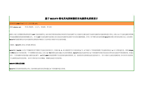
MAX1631工作流程MAX1631工作流程:1, 插上电源适配器,16V电压输出一路至待机电路高端MOS管Q16,Q18的D 极,另一路通过10Ω电阻来到MAX1631的22脚,这时芯片不工作.若22脚无16V供电,注意检修10Ω电阻是否开路或阻值变大.当1631的23脚接到为高电平(3.3V-5V)的总开启信号后,芯片开始待机.待机时21脚产生VL电压5V,9脚输出基准电压2.5V若23脚无3.3V,请检修与该脚相连的元件:如电阻,二极管,控制芯片等VL5V电压分成2路分别给芯片自身及其它芯片作为待机电压一路给1.8v/1.5v产生电路(MAX1845)作为其待机电压,二路通过D15(复合二极管,表面像是三极管)给了芯片BST端(18,25脚) ,作为内部高低端驱动器的激励供电.当VL < 5v时,芯片本身有损坏或外围负载有短路.(比如MAX1845芯片坏)当VL > 5V时,芯片本身有损坏或外接电容虚焊或人为弄掉.(IBM R31的通病) 当VL = 5V,而9脚 < 2.5V时,为芯片损坏,当VL = 5V,待机时9脚 = 2.5V,但在按下开关时为0V,说明3M或5M负载有短路. 只有VL5V正常后,9脚2.5V才会正常.这时19脚,24脚都有5V直流电压输出(工作时为低端驱动器脉冲方波输出当(7),(28)接收到3.3V或5V高电平(3M_ON,5M_ON开启信号)且保持不变时,芯片开始正常工作,内部的四个驱动器输出方波脉冲去推动外部所接的4个场效应管导通工作,输出3.3V和5V当(7),(28)无高电平时,请根据线路找到相连的芯片或元件.IBM的开启信号控制芯片是PMH4和TB62501.其他品牌的由IO芯片或H8或M38867系列芯片控制.检修时要先检修该芯片的工作条件(供电,时钟)6, 5M输出电压经变压器L3,和D32升压变为15V(VDD15),输出给光驱,USB的电压调整MOS管的控制极,以及TB62501的25脚.当输出电压或负载电流发生变化,其变化会通过9脚REF2.5V经CSH、CSL、FB 引脚反馈给芯片内部,内部自动调整方波幅度及脉宽大小,最终达到3.3V、5V 电压的稳压输出.当负载过压或过流时,其反馈会让芯片自动切断输出,最终达到保护负载及电源本身的目的。

IBM笔记本维修资料--笔记本电脑系统供电单元电路(转载)系统供电芯片型号有:一、美信产的用的最多的两个芯片MAX1632、MAX1635可以互换,它们的工作原理一样。
主要产生出3.3V 、5V 、12V电压。
二、MAX1631、MAX1634、MAX1904这三种芯片的工作原理与MAX1632 MAX1635差不多,但不能与MAX1632 MAX1635芯片互换。
说明:1、MAX1631、MAX1634、MAX1904互相可以代换。
2、MAX1631、1634、1904没有12V输出,这一点与MAX1632、1635不一样,如果MAX1631、1634、1904的板子上需要12V的话,一般是在5V输出的后级,电路中设计一个升压电路。
(参考升压电路一节)3、MAX1632、1635芯片上的12#、3#的反馈信号脚没有使用,但MAX1631、1634、1904还使用了这个反馈角。
4、4#、5#的定义与MAX1632、1635不一样。
三、MAX785 MAX786用于东芝的笔记本电脑PⅡ PⅢ较多。
四、LTC1628用于索尼、康柏的笔记本较多。
系统供电电路维修方法与经验小结:1、23PIN有总控制SHDN时?9PIN2.5V不正常或9PIN为0V 时 ? 芯片坏或者18PIIN、25PIN 5V供激放供电没有查D1与D22、7# 28#应有5V高电平控制信号,有时为NQ送来,有时与21#相连,由21#5V电压作为控制信号用,还有的由键盘芯片送来。
注:7#与28#加上一个5V的控制信号,电路应该有正常3.3V或5V 电压输出,如果还没有,一般是芯片损坏。
3、先不加电测对地阻值,首先测高端管是否击穿,供电负载是否击穿,如果是OΩ表明击穿短路了,如果有正常的几百欧阻值,但一加电就短路,表明是稳压二极管已经保护了,这是高端还管击穿的结果。
4、电源控制器芯片本身损坏的故障现象:①供电和控制都正常,但没有输出。

电路设计中的电源管理电路设计电源管理电路设计的原理和应用电路设计中的电源管理电源管理是电路设计中非常重要的一部分,它负责对电路中的电源进行管理和控制,保证电路在正常工作范围内稳定供电。
本文将介绍电源管理电路设计的原理和应用。
一、电源管理电路设计原理1. 电源管理电路的分类电源管理电路根据其功能和性质可以分为多种类型,常见的包括:稳压电源、电池管理电路、过压保护电路、欠压保护电路、过流保护电路、过热保护电路等。
每种电源管理电路都有其特定的设计原理和应用场景。
2. 稳压电源设计原理稳压电源是电路中常用的一种电源管理电路,其主要功能是保持输出电压的稳定。
常见的稳压电源设计包括线性稳压电源和开关稳压电源。
线性稳压电源的原理是通过稳压芯片将输入电压降低到所需的输出电压,然后再通过放大器将电流放大并加以稳定。
开关稳压电源则通过开关原件将输入电压进行调制,控制输出电压的稳定性。
3. 电池管理电路设计原理电池管理电路主要用于对电池进行充电和放电的控制,以及电池电量的监测和保护。
常见的电池管理电路包括充电管理电路、放电管理电路和电池保护电路。
充电管理电路通过控制电流和电压,对电池进行安全、高效的充电;放电管理电路则可以根据电池的工作状态进行放电控制,延长电池的使用寿命;电池保护电路则负责监测电池的电压、温度等参数,一旦发现异常情况,及时采取保护措施,防止电池损坏。
二、电源管理电路的应用1. 通信设备中的电源管理电路在通信设备中,电源管理电路的设计尤为重要。
通信设备通常需要多个电源来同时供电,而不同的电源需要不同的电压和电流特性,因此需要设计合适的电源管理电路来满足这些需求。
同时,通信设备的电源管理电路还需要具备过压、欠压、过流等保护功能,以确保设备的安全和稳定运行。
2. 汽车电子中的电源管理电路汽车电子由于工作环境的恶劣和电源的复杂性,对电源管理电路的要求更高。
电源管理电路在汽车电子中起到了至关重要的作用,能够保证电路的稳定供电,同时承担着电源保护、电池管理等功能。
电源管理电路设计与优化一、引言近年来,随着无线设备和便携电子产品的不断普及,对于电源管理电路的设计和优化需求日益增长。
电源管理电路是电子设备中关键的组成部分,其功能是对输入电源进行处理和转换,以满足各个组件的电源需求,同时保证系统的稳定性和高效性。
本文将针对电源管理电路的设计与优化进行探讨,总结出一些实用的方法和技巧,帮助提升电路性能和效率。
二、电源管理电路的设计要点1. 输入电源的选择与滤波电源管理电路的设计从输入端开始,合理选择适合系统的输入电源,通常有交流电源和直流电源两种选择。
在选择好输入电源后,还需要考虑使用滤波电路对输入信号进行滤波处理,以减小电源噪声对系统的影响。
2. DC-DC转换与稳压DC-DC转换是电源管理电路最常见的功能之一,通过DC-DC转换器可以将输入电源转换为适合系统组件工作的电压。
在选择DC-DC转换器时,需要考虑电流输出能力、效率、纹波噪声等因素。
此外,稳压功能也是电源管理电路必备的一部分,通过添加稳压模块可以确保输出电压的稳定性,避免对系统的不良影响。
3. 电池管理对于便携式电子产品而言,电池管理是至关重要的。
设计一个高效的电池管理电路可以有效延长电池寿命,并提供稳定的电源供应。
其中,包括充电管理、放电管理、电池保护等功能的设计与优化。
4. 低功耗设计随着对便携电子产品续航时间要求的提高,低功耗设计成为电源管理电路设计中的重要环节。
通过降低待机功耗、优化工作模式等方式,可以有效降低功耗,提升设备的续航时间。
三、电源管理电路的优化方法1. 考虑系统整体需求在进行电源管理电路设计和优化时,需要全面考虑系统的整体需求。
了解各个组件对电源的要求,合理规划电源管理电路的拓扑结构和工作模式,以满足系统性能的要求。
2. 选用高效稳定的元器件选用高效稳定的元器件是优化电源管理电路的关键。
通过选用低压降、低纹波噪声、高转换效率的电容、电感、二极管等元器件,可以有效减小功耗,提升系统效率。
什么是电源管理器如何设计一个电源管理器电路电源管理器(Power Manager)是一种用于监控和控制电源供应的设备或电路,它的主要功能是确保电源能够高效稳定地供应给各个电子设备,并且能够进行合理的功耗管理。
本文将介绍电源管理器的基本原理和设计方法。
一、电源管理器的基本原理电源管理器的基本原理是通过监控、调节和保护电源供给,并协调各个电子设备的电源需求,实现对电源的有效管理。
1.1 监控电源状态电源管理器需要实时监控电源的状态,包括输入电压、输出电压、输出电流等参数。
通过对这些参数的监测,可以及时发现电源工作异常或过载情况,并采取相应的保护措施,确保电源的稳定性和安全性。
1.2 调节电源输出电源管理器可以通过调节电源输出的电压和电流,满足不同电子设备的需求。
例如,在一些电子设备中,需要提供不同电压的电源给不同的电路模块,电源管理器可以根据电路模块的需求,调节输出电压的大小。
1.3 保护电源和电子设备电源管理器需要具备保护电源和电子设备的功能。
当电源超出工作范围或出现故障时,电源管理器可以通过监测电流、电压等参数,及时切断电源供给,避免对电子设备的损坏。
二、电源管理器的电路设计方法设计一个电源管理器的电路需要考虑多方面的因素,包括电源类型、电源输入和输出参数、保护机制等。
下面介绍一种常见的电源管理器电路设计方法。
2.1 电源选择与整流首先需要选择适合的电源类型,如交流电源或直流电源。
接下来,针对所选电源类型设计电源整流电路,将交流电源转换为直流电源,以供后续电路使用。
2.2 电压调节与稳定在电源管理器电路设计中,电压调节和稳定是重要的环节。
可以采用稳压模块(Voltage Regulator Module)来实现电压调节和稳定功能。
根据输出电压的需求,选择合适的稳压模块,并进行相应的连接和调试。
2.3 运算放大与反馈控制为了实现电源输出的准确调节,常常需要运用运算放大器和反馈控制的技术。
通过采集输出电压或电流的信息,与设定值进行比较,并通过反馈控制的方式来调节输出电压或电流的大小,实现精确的电源管理。
PARTTEMP. RANGE BOARD TYPE MAX1630EVKIT-SO 0°C to +70°C Surface Mount MAX1631EVKIT-SO 0°C to +70°C Surface Mount MAX1632EVKIT-SO0°C to +70°CSurface Mount19-1211; Rev 0; 3/97MAX1630/MAX1631/MAX1632 Evaluation Kits_______________General DescriptionThe MAX1630/MAX1631/MAX1632 evaluation kits (EV kits) each consist of one of three preassembled and tested evaluation boards (EV boards) that embody thestandard application circuits. The MAX1630 andMAX1632 EV boards provide the triple-output 3.3V/5V/ 12V circuit, and the MAX1631 EV board provides the dual-output 3.3V/5V circuit.All three use the same PC board but have different components to accommodate different input voltage ranges. The main differences between the MAX1630 and MAX1632 EV boards are in the turns ratio (1:4 or1:2.2) and in the location of the transformer connection (3.3V side or 5V side). Connecting the transformer to the 3.3V side allows lower input voltage. Connecting the transformer to the 5V side provides slightly better efficiency and lower stress voltages.These circuits are configured to deliver up to 3A of out- put current on each of the main PWM outputs with greater than 90% efficiency. The MAX1630/MAX1631/ MAX1632 EV kits can also be used to evaluate other output voltages.____________________________Featur esBattery Range: 5.2V to 20V (MAX1630)5.2V to 28V (MAX1631)6.5V to 28V (MAX1632) Outputs: 3.3V at 3A 12V at 120mA5V at 3A 5V at 30mA Keep-Alive 1:4 Transformer (MAX1630)1:2.2 Transformer (MAX1632)Adjustable 2.5V to 5.5V Outputs (optional resistor divider) Precision 2.5V Reference Output Oscillator Sync InputLow-Noise Mode Control Input (SKIP ) Power-Good Monitor (RESET output) Fully Assembled and Tested______________Or dering InformationCommon to All Thr ee EV KitsMaxim Integrated Products 1For free samples&the latest literature:,or phone1-800-998-8800DESIGNATION QTY DESCRIPTIONC412.2µF, 25V tantalum capacitor Sprague 595D225X0025B2BC110OpenD211A, 100V, fast-recovery diode Nihon EC11FS1 orMotorola MBRS1100T3D40OpenJU1, JU3–JU6,JU8,JU10,JU1182-pin headers JU51ShuntL2110µH power inductorSumida CDRH125-100 (shielded)or Coiltronics UP2-100 orCoilcraft DO3316P-103T1110µH,1:4transformer Transpower Technologies TTI-5902U11MAX1630 (SSOP-28) Maxim MAX1630CAIDESIGNATION QTY DESCRIPTION C40OpenC1112.2µF, 25V tantalum capacitor Sprague 595D225X0025B2BD411A, 100V, fast-recovery diode Nihon EC11FS1 orMotorola MBRS1100T3L1110µH power inductorSumida CDRH125-100 (shielded)or Coiltronics UP2-100 orCoilcraft DO3316P-103T2110µH,1:2.2transformer Transpower Technologies TTI-5870JU1, JU3–JU6,JU8,JU10,JU1182-pin headers JU51ShuntU11MAX1632 (SSOP-28) Maxim MAX1632CAIMAX1630/MAX1631/MAX1632Evaluation KitsMAX1630EV Kit Additional ComponentsMAX1631EV Kit Additional Components Component SuppliersMAX1632EV KitAdditional Components*Note:Please indicate that you are using theMAX1630/MAX1631/MAX1632 when contacting these componentsuppliers.2MAX1630/MAX1631/MAX1632Evaluation KitsQuick Star t The MAX1630/MAX1631/MAX1632EV kits are fullyassembled and tested. Follow these steps to verify board operation. Do not turn on the power supply until all connections are completed. 1) Connect a bench power supply(50W or better) tothe VIN and GND pads at the edge of the board.2) Connect voltmeters and loads (if any) to the VOUTpads.3) Verify that switch SW1 positions SHDN, ON5, andON3 are on, and that the shunt is across JU5.4) Turn on the power supply and verify that the outputvoltages are 3.3V and5V.Detailed DescriptionOutput Voltage The main output voltages come preset to 3.3V and5V. Install resistors R6/R7and R12/R13 for adjustable mode. Two small PC trace jumpers, JU9 and JU7,shunt FB3 and FB5 to GND on the board. These default jumpers must be cut for adjustable-mode operation. Refer to the MAX1630–MAX1635data sheet for instructions on calculating R6/R7and R12/R13.Donot operate the circuit without a jumper or resistor- divider installed, or output overvoltage will damage the IC.In addition to the standard components, the extra pull- up and pull-down resistors listed below are used to set logic input levels. These resistors can usually be omit- ted in the final design.R6,R7Adjustable-mode resistor-divider (not in- stalled). V OUT =2.5V (1 +R6 / R7).R12,R13Adjustable-mode resistor-divider (not in- stalled). V OUT =2.5V (1 +R12 / R13).R1–R42MΩlogic pull-down resistors. Shorted out or driven by logic.R14100kΩSYNC pull-up resistor (usually short ed out). SYNC to VL.Jumper Selection The three 2-pin headers JU3, JU4, and JU5 select the power-up sequence mode. Table 1 lists the selectable jumper options.The 2-pin header JU6 selects the operating frequency. Table 2 lists the selectable jumper options. The EV kit’s components are selected for 300kHz operation. C omponent values might need to be changed if200kHz operation is selected (refer to the DesignProcedure section in the MAX1630–MAX1635 data sheet). Synchronize the oscillator to an external clock signal by driving the SYNC pad with a pulse train of 5V amplitude in the 240kHz to 350kHz frequency range.Table1.Jumper JU3,JU4,JU5FunctionsAdditional Jumpers(MAX1631Only) Additional jumpers on the board along with R10 and R11 are for configuring the MAX1631 for an auxiliarysecondary output. R10and R11 set the secondaryfeedback voltage (refer to the MAX1630–MAX1635data sheet). Table 3 lists the MAX1631 jumper settings.3MAX1630/MAX1631/MAX1632Evaluation Kits 3D6CMPD2838 R L N1C210.1μFR1910ΩC244.7μF35V2225V+217T1/L1R16C10.1μFBST327DH3D7R6OPENC20220μF10V220μF10VVIN3D1R15N226LX324DL3FB3R7 OPEN 87651Figure1.MAX1630/MAX1631/MAX1632EV Kit Schematic 4MAX1630/MAX1631/MAX1632Evaluation KitsC230.01μFJU11C220.1μFJU10C1510μF30VC250.1μFC161030V12OUTC7 0.1μF R18VDDN3T2/L2D471031C112.2μF4.716VRAW+15VJU1VDDR17D5N4R80.020Ω 25V R10R11OPEN OPEN1215JU36JU4JU5VLC14VL4.7μF16V+2.5VR145MAX1630/MAX1631/MAX1632 Evaluation KitsFigure 2. MAX1630/MAX1631/MAX1632 EV Kit ComponentPlacement Guide —Component Side Figure 3. MAX1630/MAX1631/MAX1632 EV Kit Component Placement Guide —Solder SideFigure 4. MAX1630/MAX1631/MAX1632 EV Kit PC BoardLayout —Component Side6MAX1630/MAX1631/MAX1632 Evaluation KitsFigure 5. MAX1630/MAX1631/MAX1632 EV Kit PC BoardLayout —Internal GND Plane Figure 6. MAX1630/MAX1631/MAX1632 EV Kit PC Board Layout —Internal Voltage PlaneFigure 7. MAX1630/MAX1631/MAX1632 EV Kit PC BoardLayout —Solder Side7MAX1630/MAX1631/MAX1632Evaluation KitsNOTESMaxim cannot assume responsibility for use of any circuitry other than circuitry entirely embodied in a Maxim product. No circu it patent licenses areimplied. Maxim reserves the right to change the circuitry and specifications without notice at any time.8Maxim Integrated Products,120San Gabriel Drive,Sunnyvale,CA94086(408)737-7600©1997Maxim Integrated Products Printed USA is a registered trademark of Maxim Integrated Products.。
第30卷 第5期2007年10月电子器件Ch inese Jou r nal Of Elect ro n DevicesVol.30 No.5Oct.2007Design of L ED Measur ement Instr ument B a sed on Ma x16473L O N G Xi n g 2mi n g1,2,Z H OU J i n g21.P hysics Dept .of Chongqin g Nor mal Uni versi t y ,Chon gqi n g 400047,Chi na;2.EE Dep art ment of Chongqi ng Univers it y ,Chongqin g 400044,Chi naAbstract :A para met ers measurement system of Li ght Emi tt ing Diode (L ED )elect ronic ,color a nd spat ial is gi ven to ove rco me t he di sadvant ages of t he exi st ed L ED measurement tools :low int elli gence ,mono 2f unc 2t ion and i nefficie ncy.U si ng t he powe r manger Max1647,t he hi gh accurat e di gital cont rol led const ant cur 2rent/vol tage L ED driver wi t h abilit y of 4.096A ,is reali zed in step of 1mA .Co mbini ng ful l f unctional si n 2gle 2c hip microcomp ut er C8051F020wit h const ructed opt ical 2elect ronic processi ng met hod and Human 2PC i nte rface met hod ,a real 2time L ED measuring syst em was realized.The practical application shows t ha t t he developed L ED measurement syst em i s convenient and efficie nt in measuring t he L ED paramet er s.K eyw or ds :semiconductormeasurementtechnology;L EDmeasurement ;MAX1647;di gitalcont rolled driverEEACC :1210基于M AX 1647的L ED 参数测试仪驱动电路设计3龙兴明1,2,周 静21.重庆师范大学物理系,重庆400047;2.重庆大学电气工程学院,重庆400044收稿日期622基金项目重庆市教委资助(K 68)作者简介龙兴明(62)男,讲师,博士研究生,研究方向为L D 照明技术、光电信号检测,y @63摘 要:针对半导体发光二极管(L ED)参数检测仪器还比较欠缺的现状,提出可以实现L ED 光、色、电性能的全性能、高精度测试驱动电路.通过利用M AX 1647电源管理芯片的数控恒流/恒压特性,设计了驱动能力为4.096A ,步长为1mA 的L ED 供电电路,结合C8051F020的内部特性,实现了光电转换信号的采集,光谱分析步进电机同步驱动,并且提供了友好的L CM 接口界面和上位PC 机的串口通讯.在实际的LED 参数测试中,证明了该驱动电路设计不仅高效、安全、可靠,而且大大的提高了整个系统的智能化程度.关键词:半导体测试技术;L ED 参数检测;MAX1647;数控恒流中图分类号:TN 206 文献标识码:A 文章编号:100529490(2007)0521754204 近年来,L ED 的开发、生产和应用得到快速的发展.L ED 具有发光强度高、功耗低、可靠性高、易驱动、小巧等优点,已被广泛应用于城市景观装饰、交通车站和商业广告等公众设施.然而,L ED 的输出光强和波长具有分散性,并且各性能参数可能随时间和工作温度的变化而变化,这使得它作为一般照明推广仍然存在挑战.因此,L ED 参数的测试对生产研发有着重要的指导意义.目前,市面上的L ED 参数测试大都采用手动完成,在对大量样品进行参数检测分析时,效率非常低下.本文分析了L ED 参数的特点,提出基于功能强大的电源管理芯片MAX1647的数控恒流驱动,设计了集单片机技术,传感器技术以及光电信号分析技术于一体,实现L ED 参数测试智能化、一体化的驱动电路,有效地提高了L ED 参数测试的速度和效率.:2000929:J 0009:197E len n d rago n 1.co m.1 整机驱动电路设计根据L ED性能参数指标及单晶片单管L ED低电压、大电流驱动的发展趋势,L ED参数测试指标可分为以下三类:(1)电参数测试:正向工作电流0~4096mA、步长为1mA;正向工作电压0~20V;反向击穿电压0~400V;反向漏电流测量;(2)空间光强分布测试:光度光强:0~200000 mcd;发射角度:0°~180°;2π光通量:0~1000l m;(3)色参数测试:波长范围:380~780nm;自动获取峰值波长、光谱半宽度等参数.因此,相应地设计三个测试模块驱动电路:电性能参数测试驱动电路、空间光强分布测试驱动电路、色参数测量驱动电路;另外还包括键盘、LCM等辅助功能模块.我们选择沈阳新华龙电子有限公司的C8051F020单片机为系统的核心器件(以下简写为: F020).F020单片机内部包含12bit DAC转换器、5个通用16bit定时器、内部可编程振荡器、低功耗、128kbyt e的非易失数据存储以及丰富的I/O资源等,它是一个性能优良的单片机芯片,可以有效的减少硬件电路的复杂性.整体驱动电路框图如图1所示.图1 LED参数测试驱动电路总体框图电性能参数测试驱动电路主要完成正向工作电流与正向工作电压变化关系、反向击穿电压、反向漏电流的测量.该功能具体由数控电流芯片max1647,反向击穿电压升压电路,电压/电流取样电路以及F020采集处理电路具体完成.比如,当测量正向工作电流———电压特性时,根据F020的设定值确定ma x1647数控恒流输出的范围和步长,并对测试L ED样品进行供电,与此同时利用F020的A/D转换器记录下相应电流的L ED压降大小.空间光强分布测试驱动电路主要完成发射角度测量、光强和光通量随电流变化关系的测量,包括x6数控恒流,积分球,准直透镜系统,步进电机旋转机构,光电转换、放大,F的采集处理对于电流———光通量特性测量,首先由F020控制max1647输出满足测试L ED的电流范围和步长,然后利用积分球对输出光进行混光,并在积分球的窗口处利用硅光电二极管实现光电转换;最后利用F020的A/D转换采集该电流下的光电转换结果.色参数测量电路主要完成光谱曲线采集,包括max1647数控恒流,平面光栅(光谱分析),步进电机控制,光电转换、放大,F020的采集处理.设定电流下的L ED输出光束经过光栅分光后,把入射的复合光分解为单色光照在光电探测器上,此时,光栅转过的角度对应一定波长的单色光,光电探测器上的电压对应着该单色光的强度.其中,光栅转动的角度由步进电机的运动控制.因此,驱动电路的设计主要从以下几个方面进行描述:①max1647数控恒流/恒压电源的设计;②光电转换和步进电机驱动电路;③输入输出接口;其中,满足需要的数控恒流/恒压电源和光电转换电路设计是本系统精度和自能化高低的关键和重点.1.1 max1647数控恒流/恒压源MAX1647是MA XIM公司的新型电源管理芯片,它包括一个电压调整环与一个电流调整环,内部有一个6bit电流预置D/A转换器和10bit的电压预置D/A转换器,最大电流输出为4.096A并且具有恒流与恒压以及自动转换功能;采用IN TEL系统管理总线(SMBU S)接口.MA X1647的输出特性曲线如图2.图2 MAX1647的输出特性曲线当输出电压小于预置电压V0时,电流调整环发挥作用,输出是恒流模式;当负载的电压到达预置电压V0以后,电流调整环停止作用,电压调整环开始工作,这时输出为恒压模式.1.1.1 L ED数控电源驱动电路设计数控电源驱动电路使其输出电流/电压满足L ED电参数测试指标的驱动范围,并且输出电流/电压具有程序可预置功能.基于MAX1647的L ED数控驱动电路如图3.M X6的WM输出端子LD和D I分别控制两个场效应管Q和Q,经同步整流、滤波器滤波后,得到所需的输出信号输出电流电压检测5571第5期龙兴明,周 静:基于MAX1647的L ED参数测试仪驱动电路设计ma147020.A147P P H01./图3 L E D数控驱动电路结果由反馈输入CS/BA TT引脚引入,结合F020的预置电压/电流实现设定恒流/恒压输出.1.1.2 F020对MAX1647的控制F020通过SMBU S的R EAD2WORD和WRI TE2WORD协议与MAX1647进行双向通信,实现参数的设置.F020与MA X1647通信的开始条件是SDA端口为下降沿,同时SCL端口为高电平; MAX1647的WR IT E2WORD协议为0x12(0x表示十六进制),R EAD2WORD协议为0x13.另外,命令由CMD0~CMD7表示,当命令位为0x12时,完成内部清零和复位;0x15表示电压预置命令;0x14表示电流预置命令;设置的电压/电流大小由16位二进制数D15~D0组成表示.本电路SEL端子与VL 短接,则I0的最大预置值为4.095 A.因此, MAX1647数据位D11~D6对应为6位电流预置DAC的DA5~DA0位;数据位D4~D0对应内部提供的线性电流源二进调整数.为了满足SMBU S的通信规则,我们用单片机P1口的其中两位分别模拟数据信号SDA和时钟信号SCL,F020的P1.1口与MAX1647的SCL端子连接,P1.0口与MAX1647的SDA端子连接.F020与MA X1647相互通信的部分代码如下:;设置电压V0子程序.(设置电流I0时,42h,43h单元分别为35h,36h)chargv:mov r0,#40h;预置电压数据存在40H、41H中mov40h,#12hmov41h,#15hmov42h,33hmov43h,34hlcall writ ew,把设置的数据写入MAX1647;写数据子程序,#3,@;读待写数据或命令se tb p1.1;开始与MAX1647通信se tb p1.0clr p1.0ext w1:mov sbuf,a;逐位写入.jbc ri,extwlinc r0mov a,@r0djnz r2,extw1ret1.2 光电转换及步进电机驱动在光、色参数测试模式下,L ED输出光先经光电二极管转化为微弱模拟电信号,然后经过高精度的仪表放大器MA X4197放大,最后由F020内部12位A/D转换器进行采样.在光电转换电路中,考虑到实测波段范围在380~780nm,故光电转换传感器选用电子工业部24所生产的低噪、高放大硅光电二极管.根据提供的参数,为进一步降低其暗电流,并保证一定的准确度,我们采用-24V的偏压.考虑到负载电阻的分压效应,负载电阻不宜太大,取200Ω比较适合.另外,步进电机控制是光、色参数测试的重要机构.它包括起/停、前进、后退、转速等控制等功能(其中,单片机的P1.4口负责产生驱动方波、P1.3口负责方向控制).同时,为了提高单片机的稳定性,在驱动电路与单片机之间增加光电隔离电路.1.3 输入输出接口一方面,为了整个系统可以工作在单机状态下,即不需要上位机支持.我们用136键盘直接连在F020单片机P7的5个端口上,结合1283 64MG L S212864液晶显示模块实现友好的界面显示.其中,L CM的操作利用直接控制方式由P1口作为数据端口,P3口作为控制端口.另一方面,结合PC机的虚拟仪器编程技术,我们通过RS232把F020采集的数据打包处理,送入PC机.单片机与PC机之间的通信必须进行电平转换,将T TL电平转换成R S2232电平.用一片MAX232专用转换芯片可达到此目的.2 测试实验我们利用提出的驱动电路,结合美国NI公司推出的虚拟仪器编程语言L abWindow s/CVI设计了虚拟分析功能,整个软件系统分为:文件管理,数据预处理,串口设置,色参数测试,空间参数测试和电参数测试等模块把该系统应用于泰富照明制造有限公司的大量L D样品参数测试中,结果令人非常满意6571电 子 器 件第30卷retwritew:mov r2mov a r0.E.一方面,大大提供了测试速度,并且数据测试结果易于保存;另一方面,降低了工人测试过程中由于疲劳引起的误差,提高了参数的可对比性.图4为明学封装的Φ5高亮L ED实际测试的测试结果,从分析系统界面上可以直观快速的得到相关参数.从这些图我们可以确定相应得光电参数特性,通过移动各界面分析界面的光标知,当电流为18mA时,对应的光强为4.710cd;电流为17mA时,对应的光通量为3.52lm;样品PN 结温度为25℃,电流为20mA时的配光曲线图(直角坐标),从该曲线可得发射角为36o,并且说明峰值强度不在机械轴的中心位置.图4 从上到下,从左到右:正向电流/电压图,光谱曲线,电流/光通量和配光曲线图3 结论本文讨论了基于MAX1647为核心的L ED测试驱动电路,通过利用C8051F020单片机实现了L ED参数测试中的光电信号的采集、步进电机控制以及数据的输入输出功能.实际应用证明,由于引入了数控恒流/恒压芯片使得建议的L ED测试驱动方案具有功能性强、编程容易;另一方面,避免了纯硬件控制带来的复杂性,提高了L ED测试的智能性.参考文献:[1] 2006,4《L ED mont hly》[EB/OL],htt p://www.ledmont hl /.[2] Subramani an Mut hu,Sch uurmans Frank J P and Pashley Mi2chael D.Red,Green,and Blue L ED fo r Whi te Lig ht Ill u2mi n2Atio n[J].IEEE Jo urnal on S elect ed Topics i n Quan2t u m Elect ronics,March/Ap ril2002,8(2):3332338.[3] 赵良炳.现代电力电子技术基础[M].清华大学出版社,1995年第一版.[4] 龙兴明.基于L abWindows/CV I的光谱分析系统的设计与实现[J].微计算机信息,2003,19(10):60261,102.[5] Maxi m C orp,New Release Dat a[M]CD2R o m.2001.[6] 潘琢金.C8051F单片机应用解析[M].北京:北京航空航天大学出版社,2002.[7] NI公司LabWi ndo ws/CVI用户手册[S].7571第5期龙兴明,周 静:基于MAX1647的L ED参数测试仪驱动电路设计。
MAX1647电源管理电路设计详解
随着二极管泵浦全固态激光器相关技术的不断发展,它在工业、国防
科研、生物医学工程等领域的应用越来越广泛,对其输出功率、可靠性要求也
不断提高。
作为二极管泵浦全固态激光器的重要组成部分的电源,其可靠性、
稳定性也就显得格外重要。
二极管泵浦全固态激光器的电源功率较大,输出为
大电流、低电压,工作脉冲频率较高(可达1kHz),输出电流、电压的稳定性要求很高。
微小的电流扰动将影响激光器的出光质量,不当的保护可能引起巨
大的损失。
针对这些特点,我们选择功能强大的电源管理芯片MAX1647作为
整个系统控制的核心部分,设计出完全满足要求的大功率激光器电源。
MAX1647电源管理芯片介绍
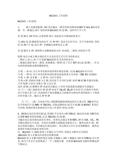
MAX1647是MAXIM公司的新型电源管理芯片,其内部结构如
在MAX1647的电压调整环中,通过SMBUS总线,经内部10位DAC 设置预置电压,负载电压与预置电压通过GMV误差放大器进行比较放大后的
误差信号输出到CCV端口,然后送到一个由二选一电路组成的恒流/恒压自动
转换电路的一个端子上,其中由CCV端口输出的误差信号由内部钳位电路限
制在1/4到3/4参考电压之间的;与电压调整环工作原理相类似,被钳位的电
流误差信号由CCI端口送到自动转换电路的另一个端子上;利用PWM控制器,把电压/电流误差信号转换为脉宽调制信号,用以驱动两个N沟道MOSFET管,经同步整流、滤波器滤波后,得到所需的输出信号。
MAX1647的输出特性曲线如整体电路设计
整体电路设计框
MAX1647电源管理芯片是整个系统的控制核心部分,它完成恒流、恒
压及相互之间自动转换的功能。
但MAX1647的最大输出4A,不足以达到设计。