第二节STR-W6553A电源简介
- 格式:pdf
- 大小:74.69 KB
- 文档页数:3
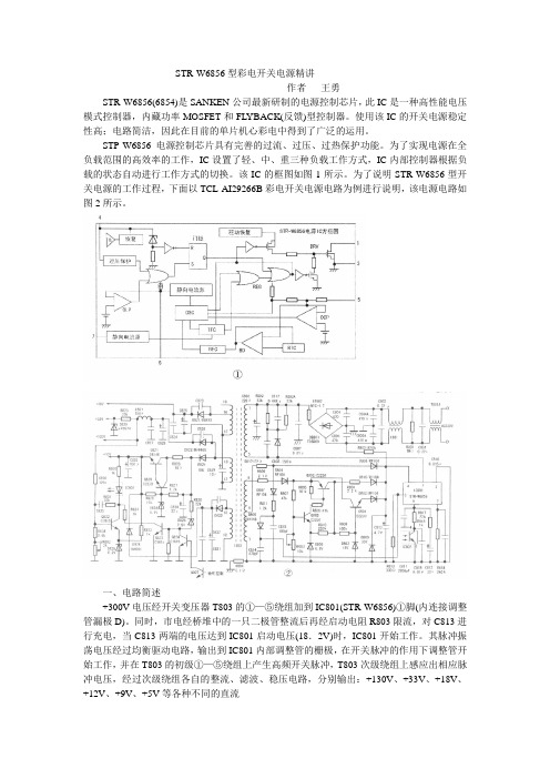
STR-W6856型彩电开关电源精讲作者王勇STR-W6856(6854)是SANKEN公司最新研制的电源控制芯片,此IC是一种高性能电压模式控制器,内藏功率MOSFET和FL YBACK(反馈)型控制器。
使用该IC的开关电源稳定性高;电路简洁,因此在目前的单片机心彩电中得到了广泛的运用。
STP-W6856电源控制芯片具有完善的过流、过压、过热保护功能。
为了实现电源在全负载范围的高效率的工作,IC设置了轻、中、重三种负载工作方式,IC内部控制器根据负载的状态自动进行工作方式的切换。
该IC的框图如图1所示。
为了说明STR-W6856型开关电源的工作过程,下面以TCL-AI29266B彩电开关电源电路为例进行说明,该电源电路如图2所示。
一、电路简述+300V电压经开关变压器T803的①—⑤绕组加到IC801(STR-W6856)①脚(内连接调整管漏极D)。
同时,市电经桥堆中的一只二极管整流后再经启动电阻R803限流,对C813进行充电,当C813两端的电压达到IC801启动电压(18.2V)时,IC801开始工作。
其脉冲振荡电压经过均衡驱动电路,输出到IC801内部调整管的栅极,在开关脉冲的作用下调整管开始工作,并在T803的初级①—⑤绕组上产生高频开关脉冲,T803次级绕组上感应出相应脉冲电压,经过次级绕组各自的整流、滤波、稳压电路,分别输出:+130V、+33V、+18V、+12V、+9V、+5V等各种不同的直流稳压电源,供给整机各部分使用,其中:+130V主电源,主要供给行扫描输出电路工作;+33V调谐电压,主要供TU调谐工作;+18V电压,主要供IC601伴音功放电路工作;+12V 电压经IC803 (L7809) 和IC804(L7805)稳压后输出+9V和+5V直流电压,供芯片小信号处理电路工作。
二、单元电路分析1.电源启动电路通电后,AC220V市电经半波整流、K803限流、C813滤波后给IC801④脚供电,如图3所示。

使用说明书OPERATIONMANUALTH6300系列单路线性自动范围可编程DC电源TH6303 AUTO RANGE DC POWER SUPPLY***********目录第1章概述 .......................................................................................................................... 1-11.1引言 .......................................................................................................................... 1-11.2使用条件 ................................................................................................................... 1-11.2.1电源 .............................................................................................................. 1-11.2.2环境温度与湿度................................................................................................ 1-21.2.3预热 ................................................................................................................. 1-2第2章几点注意问题............................................................................................................ 2-12.1体积与重量................................................................................................................ 2-12.2安全要求 ................................................................................................................... 2-12.2.1绝缘电阻 .......................................................................................................... 2-12.2.2绝缘强度 .......................................................................................................... 2-12.2.3泄漏电流 .......................................................................................................... 2-12.3电磁兼容 ................................................................................................................... 2-22.3.1电源瞬态敏感度按GB6833.4的要求。


科技成果——除尘用STR03系列高频电源适用范围该技术可配套各类除尘设备,广泛应用于电力、冶金、建材、轻工、化工等众多行业的烟气粉尘治理。
技术原理除尘用STR03系列高频电源原理图该技术的基本原理如图所示,采用的总体的技术方案为:三相交流电源输入-整流-高频谐振逆变-升压整流输出直流高压。
该技术通过调节供电方式给除尘器提供接近纯直流到脉动幅度很大的各种电压波形,工况适应性强。
纯直流供电时,通过调节高频逆变环节的开关频率调节输入到变压器的谐振电流平均值,从而调节设备的输出电压,纯直流供电输出电压纹波小于3%,适用于中低比电阻粉尘工况。
间歇供电时,设备开关频率可以调节,同时通过控制逆变电路开通Pon 和关断Poff的时间,实现间歇供电,间歇比任意可调,可有效抑制反电晕现象,实现保效节能,特别适用于高比电阻粉尘工况。
工艺流程该技术的工艺流程是:将三相380V交流电源通过整流桥后输出直流电源,并采用滤波电感和直流支撑电容降低交流脉动波纹系数使输出直流电压平滑。
直流电源经逆变器逆变为高频交流电源,逆变器采用串联谐振拓扑结构具有恒流特性,在输出短路时有极好的限流能力;同时采用软开关控制技术,有效降低器件的关断应力,开关损耗小;设计合理的叠层母排式布置结构有效降低线路分布电感提高功率器件运行的可靠性和稳定性。
高频交流电源经高频整流变压器升压整流后输出直流负高压给电除尘器供电,供电方式采用纯直流或间歇供电方式,该技术可针对烟气工况自动调节供电方式,提供最合适的电压波形给电除尘器供电,从而提高除尘效率。
关键技术叠层母排式大功率变换器结构降低线路分布电感提高功率器件运行可靠性及稳定性;IGBT功率器件、分立式整流模块采用热管散热技术,散热效率高;机柜热交换密封式散热技术确保控制柜防护等级达到IP55,确保高频电源在户外环境可靠应用;印刷电路板采用灌封和涂覆有机硅三防漆工艺技术,确保电路板可靠工作;大功率高频高压硅堆和变压器分布参数设计,确保高频整流变压器在大功率高频状态下可靠运行。

创维32/37寸LED电视〔LGV6屏〕通用电源一、电源方案介绍1.此液晶电源输进电压范围为AC110~240,输出电压情况为5V/、24V/2.5A、12V/三组直流电源。
2.此电源采纳Sanken公司的待机芯片STR-A6059M。
3.PFC操纵芯片FA5591与主芯片FA5641,主芯片为反激操纵芯片。
二、产品系列与机型比立表1-1产品系列与机型比立三、电源要紧特点1、本产品为自冷形式;2、有过压,过载保卫功能。
电源因过压,过载,短路时会自动进进保卫状态,当故障排除后电源需重新启动才能恢复工作;3、本电路为软驱动电路,需先开机后带重载;a、24V输出电压超过27-32.5V时进进保卫状态,12V输出电压超过13-18V时进进保卫状态;b-4A时进进保卫状态;c、有短路保卫功能。
正负极短路,电源进进保卫状态;4、电磁兼容要求。
符合GB9254B级的要求;5、电源工作效率大于80%〔输进电压为220V满载时〕;6、满载时功率因素大于0.90;四、电源组件要紧器件了解1、市电输进电路与整流滤波电路:由电感、电容组成的低通滤波器组成。
2、PFC〔功率因数校正〕校正电路,由FUJI操纵芯片FA5591组成。
3、操纵电路:这局部电路由两局部组成。
A:副电源〔+5待机开关稳压电路〕;由Sanken公司的STR-A6059M组成。
此电路为反激式电路,STR-A6059M集成了开关管MOSFET管,为集成块。
B:+24V、12V主开关稳压电路。
由FUJI芯片FA5641操纵开关管,与它操纵的开关管组成了反激式电路。
4、各操纵电路输出整流稳压电路。
输出整流电路由二极管组成的半波整流电路。
5、还有保卫电路和相应电路图1-1电源组件实物图解〔正面〕图1-2电源组件实物图解〔反面〕五、电源组件信号流程框图液晶电源都有严格的时序操纵:接通电源,副电源产生待机5V电压至主板,主板CPU开始工作,当整机处于待机状态,主板CPU接收到开机指令〔按远控器或本机按键上的开机键〕,CPU发出开机指令至电源板ON/OFF足,促使供电操纵电路工作,给主DC-DC电路和PFC电路供电,然后产生主板和背光〔恒流〕板所需要的12V和24V电压。
第二节 STR-W6553A 电源简介STR-W6553A 为内藏功率MOSFET 和控制器,以准共振方式工作的开关电源用厚膜集成电路。
通常工作以准共振或Bottom Skip 准共振动作,实现了开关电源的高效率,低噪声等优良性能,待机时以间歇振荡方式工作以降低待机功率。
使用该IC 可以大量减少电源元件的数量,简化电路的设计。
一、特点1、 在待机的状态下,当输出电压下降时电源以间歇振荡方式工作以降低待机功率。
2、 在原来的准共振工作方式的基础上增加了Bottom Skip 功能,改善了高电压输入时的电源效率。
3、电源启动时,以SOFT-START 方式启动。
4、内藏STEP-DRIVER 功能以减小开关噪声。
5、 使用SENSE-MOSFET ,不需要漏极电流检测用的电阻,且可以做到过电流保护的调整。
6、 内藏过电流保护电路,过电压保护电路,过负载保护电路,和最大的ON 时间限制电路。
7、保证MOSFET 的雪崩耐量。
二、IC 引脚介绍: 记号 名称 功能 1D MOSFET 漏极端子 开关管漏极D 2NC3S/GND MOSFET 源极端子/GND 控制器GND 4VCC 电源端子 启动电路5 SS/ADJ SOFT-START/过电流保护调整端子6 FB 反馈端子7BD Bottom 检测端子 U n R e g i s t e r e d三、启动原理启动电路检测VCC 端子(4号端子)的电压,控制IC 的动作开始和停止。
当AC 电源输入以后,AC 输入电压通过启动电阻R803对C808充电。
当C808的电压达到启动开始电压VCC (on )=18V 时,STR-W6553A 开始工作,开关管开始有开关动作。
随着输出电压和辅助绕组电压的上升,由辅助绕组给IC 供电。
1、关于启动①由于IC 的启动电流很小,R803可使用高阻值的电阻,来降低待机功耗。
但是要注意R803要向IC 提供足够的锁定电路保持电流,特别是低电压输入的时候能向IC 提供100UA 以上的电流。
利用STR 设计34″彩色电视机开关电源摘要:介绍Sanken公司的混合型开关电源ICSTR F6600系列的原理和应用,作为实例,介绍了使用STR F6656设计一个34″彩电用的开关电源,并给出满意的实验结果。
1引言混合型电源ICSTR F6600系列是日本Sanken电气公司的近年产品。
它内含MOSFET及控制IC部分,是专门为反激型变换器设计的,特适用于彩色电视机开关电源。
该混合IC可工作于准谐振方式以及脉冲占空比控制(PRC——PulseRatioControl)方式。
它具有常规第二代SMPSIC的特点,即采用次级输出采样及光耦反馈稳压、准谐振、高效率、宽输入范围、良好的输入电压调整率和负载输出特性,还有过流、过压及热保护等。
相对于同类型的其它厂家IC,它多了一个热保护以及开关电噪声较小,可简化或甚至取消浪涌吸收电路。
本文介绍该系列IC的工作原理,在此基础上描述怎样利用它设计制造一个34″彩色电视机开关电源。
文中给出样机电源电路,变压器设计以及实验结果。
实验表明,该电源完全符合电视机电气要求,它外围元件少,设计容易,稳定度高。
在高温、低温、EMI、短路和开路等环境和安全实验中均符合国家标准,是一个不可多得的简单和高效能的电视机实用开关电源。
2混合型开关电源控制器STR F6600系列原理和特性简介图1给出了STR F6600系列的原理方框图。
这是一个有一个引出脚的塑料封装IC,其每脚功能简述见表1。
表1STR F6600系列每脚功能2 1起动电路当AC电源在t0加入时,由图2可知,在半个周期内,A点对地峰值电压VA≈Vd(整流电压),VA经过R902向C909充电,使IC脚④上电压Vin 近似线性上升(见图3)。
当Vin上升到阈值电压Vin(ON)=16V图1STR F6600系列方框图图2起动电路图3起动时Vin端口电压的波形时,IC内的控制电路开始起动,Vin端口上的输入电流Iin由100μA突升到30mA,电容C909来不及供电而使Vin下降。
DescriptionThe STR-A6059H, STR-A6061H, STR-A6062H, and STR-A6069H are power ICs for switching power supplies, incorporating a power MOSFET and a current mode PWM controller IC in one package.To achieve low power consumption, these products include a startup circuit and a standby function in the controller. The switching modes are automatically changed according to load conditions: in normal operation, PWM mode, and in light load conditions, burst mode. The rich set of protection features helps to realize low component counts, and high performance-to-cost power supply.Features and Benefits▪ Current mode PWM control▪ Brown-In and Brown-Out function: auto-restart, prevents excess input current and heat rise at low input voltage ▪ Auto Standby function: improves efficiency by Burst mode operation in light load▫ Normal load operation: PWM mode ▫ Light load operation: Burst mode ▪ No load power consumption < 25 mW▪ Operating frequency, f OSC(A VG)(typ) = 100 kHz▪ Random Switching function: reduces EMI noise, and simplifies EMI filters▪ Slope Compensation function: avoids subharmonic oscillation▪ Leading Edge Blanking functionPWM Off-Line Switching Regulator ICsTypical Application CircuitNot to scaleContinued on the next page…STR-A6000H SeriesApplications:Switching power supplies for electronic devices such as:• Battery charger• Standby power supply• Small switch-mode power supply (SMPS)• Auxiliary power supply for controllerPackage: DIP8Selection GuidePart NumberPower MOSFETOutput Power*, P OUT (W)V DSS (min)(V)R DS(ON)(max)(Ω)Open Frame Adaptor230 VAC 85 to 265 VAC 230 VAC85 to265 VACSTR-A6059H 650630191711STR-A6069H 700630191711STR-A6061H 700 3.9535242115STR-A6062H 700 2.838262318*The listed output power is based on the thermal ratings, and the peak output power can be 120% to 140% of the value stated here. At low output voltage and short duty cycle, the output power may be less than the value stated here.Features and Benefits (continued)The polarity value for current specifies a sink as "+," and a source as “−,” referencing the IC.Absolute Maximum Ratings Unless otherwise specified, T A = 25°CCharacteristicSymbolNotesPinsRating Unit Drain Peak Current 1I DPEAKSTR-A6059H STR-A6069HSingle pulse8 − 11.8A STR-A6061H2.5A STR-A6062H3.0A Avalanche Energy 2E ASSTR-A6059H STR-A6069H Single pulse, V DD = 99 V, L = 20 mH, I LPEAK = 1.8 A8 − 124mJ STR-A6061H Single pulse, V DD = 99 V, L = 20 mH, I LPEAK = 2 A 46mJ STR-A6062HSingle pulse, V DD = 99 V, L = 20 mH, I LPEAK = 2.2 A56mJ S/OCP Pin Voltage V OCP 1 − 3−2 to 6V Control Part Input Voltage V CC 5 − 332V FB/OLP Pin Voltage V FB 4 − 3−0.3 to 14V FB/OLP Pin Sink Current I FB 4 − 3 1.0mA BR Pin Voltage V BR 2 − 3−0.3 to 7V BR Pin Sink CurrentI BR 2 − 3 1.0mA Power Dissipation of MOSFET 3P D1Mounted on 15 mm × 15 mm printed circuit board8 − 1 1.35W Power Dissipation of Control Part P D2 5 − 3 1.2W Operating Ambient Temperature 4T OP –−20 to 125°C Storage Temperature T stg –−40 to 125°C Channel TemperatureT ch–150°C1Refer to MOSFET Safe Operating Area Curve.2Refer to MOSFET Avalanche Energy Derating Coefficient Curve.3Refer to MOSFET Temperature versus Power Dissipation Curve.4The recommended internal frame temperature, TF, is 115°C (max).▪ Audible Noise Suppression function during Standby mode ▪ Protection features▫ Overcurrent protection (OCP): pulse-by-pulse, with input compensation function▫ Overvoltage protection (OVP): latched shutdown ▫ Overload protection (OLP): auto-restart, with timer ▫ Thermal shutdown protection (TSD): latched shutdownElectrical Characteristics of Control Part Unless otherwise specified, T A = 25°C, V CC = 18 VCharacteristic Symbol Test Conditions Pins Min.Typ.Max.UnitOperation Start Voltage V CC(ON) 5 − 313.815.316.8VOperation Stop Voltage1V CC(OFF) 5 − 37.38.18.9VCircuit Current in Operation I CC(ON)V CC = 12 V 5 − 3–– 2.5mAMinimum Start Voltage V ST(ON) 5 − 3–38–VStartup Current I STARTUP V CC = 13.5 V 5 − 3−3.7−2.5−1.5mAStartup Current Threshold Biasing Voltage1V CC(BIAS)I CC = −100 μA 5 − 38.59.510.5VAverage Operation Frequency f OSC(AVG)8 − 390100110kHzFrequency Modulation DeviationΔf8 − 3–8–kHzMaximum Duty Cycle D MAX8 −3778389%Minimum On-Time t ON(MIN)––470–nsLeading Edge Blanking Time t BW––280–nsOCP Compensation Coefficient DPC––33–mV/μsOCP Compensation Duty Cycle Limit D DPC––36–%OCP Threshold Voltage at Zero Duty Cycle V OCP(L) 1 − 30.700.780.86VOCP Threshold Voltage at 36% Duty Cycle V OCP(H)V CC = 32 V 1 − 30.810.90.99VMaximum Feedback Current I FB(MAX)V CC = 12 V 4 − 3−340−230−150μAMinimum Feedback Current I FB(MIN) 4 − 3−30−15−7μAFB/OLP Pin Oscillation Stop ThresholdV FB(STB) 4 − 30.850.95 1.05V VoltageOLP Threshold Voltage V FB(OLP) 4 − 37.38.18.9VOLP Delay Time t OLP 4 −3546882msOLP Operation Current I CC(OLP)V CC = 12 V 5 − 3–300600μAFB/OLP Pin Clamp Voltage V FB(CLAMP) 4 − 31112.814VBrown-In Threshold Voltage V BR(IN)V CC = 32 V 2 − 3 5.2 5.66VBrown-Out Threshold Voltage V BR(OUT)V CC = 32 V 2 − 3 4.45 4.8 5.15VBR Pin Clamp Voltage V BR(CLAMP)V CC = 32 V 2 − 36 6.47VBR Function Disabling Threshold Voltage V BR(DIS)V CC = 32 V 2 − 30.30.480.7VVCC Pin OVP Threshold Voltage V CC(OVP) 5 −3262932VLatch Circuits Holding Current2I CC(LATCH) V CC = 9.5 V 5 − 3–700–μAThermal Shutdown Temperature T j(TSD)–135––°C1V CC(BIAS) > V CC(OFF) always.2A latch circuit is a circuit operated with Overvoltage Protection (OVP) and/or Thermal Shutdown Protection (TSD) in operation.Electrical Characteristics of MOSFET Unless otherwise specified, T A is 25°CCharacteristic Symbol Test Conditions Pins Min.Typ.Max.UnitDrain-to-Source Breakdown Voltage V DSS STR-A6059H8 – 1650––V STR-A6061HSTR-A6062HSTR-A6069H700––VDrain Leakage Current I DSS8 – 1––300μAOn-Resistance R DS(ON)STR-A6059HSTR-A6069H8 – 1––6ΩSTR-A6061H–– 3.95ΩSTR-A6062H–– 2.8ΩSwitching Time t f8 – 1––250nsThermal Resistance Rθch-C The thermal resistance betweenthe channels of the MOSFET andthe case. Case temperature, T C, ismeasured at the center of the casetop surface.–––22°C/WTime (s)1010.10.0110-610-510-410-310-210-1T r a n s i e n t T h e r m a l R e s i s t a n c e , R θc h -c (°C /W )Transient Thermal Resistance CurveAmbient Temperature, T A (°C)1.61.41.21.00.80.60.40.20A l l o w a b l e P o w e r D i s s i p a t i o n , P D 1 (W )MOSFET Temperature versus Power Dissipation CurveChannel Temperature, T ch (°C)100806040200255075125100150E A S T e m p e r a t u r e D e r a t i n g C o e f f i c i e n t (%)MOSFET Avalanche Energy Derating Coefficient CurveDrain-to-Source Voltage, V DS (V)1010.10.01D r a i n C u r r e n t , I D (A )MOSFET Safe Operating Area CurveChannel Temperature, T ch (°C)100806040200 25 50 75 100 125 150S a f e O p e r a t i n g A r e a T e m p e r a t u r e D e r a t i n g C o e f f i c i e n t (%)S. O. A. Temperature Derating Coefficient CurveCharacteristic PerformanceSTR-A6059HTime (s)1010.10.0110-610-510-410-310-210-1T r a n s i e n t T h e r m a l R e s i s t a n c e , R θc h -c (°C /W )Transient Thermal Resistance CurveAmbient Temperature, T A (°C)1.61.41.21.00.80.60.40.20A l l o w a b l e P o w e r D i s s i p a t i o n , P D 1 (W )MOSFET Temperature versus Power Dissipation CurveChannel Temperature, T ch (°C)100806040200255075125100150E A S T e m p e r a t u r e D e r a t i n g C o e f f i c i e n t (%)MOSFET Avalanche Energy Derating Coefficient CurveDrain-to-Source Voltage, V DS(V)1010.10.01D r a i n C u r r e n t , I D (A )MOSFET Safe Operating Area CurveChannel Temperature, T ch (°C)100806040200 25 50 75 100 125 150S a f e O p e r a t i n g A r e a T e m p e r a t u r e D e r a t i n g C o e f f i c i e n t (%)S. O. A. Temperature Derating Coefficient CurveCharacteristic PerformanceSTR-A6061HTime (s)1010.10.0110-610-510-410-310-210-1T r a n s i e n t T h e r m a l R e s i s t a n c e , R θc h -c (°C /W )Transient Thermal Resistance CurveAmbient Temperature, T A (°C)1.61.41.21.00.80.60.40.20A l l o w a b l e P o w e r D i s s i p a t i o n , P D 1 (W )MOSFET Temperature versus Power Dissipation CurveChannel Temperature, T ch (°C)100806040200255075125100150E A S T e m p e r a t u r e D e r a t i n g C o e f f i c i e n t (%)MOSFET Avalanche Energy Derating Coefficient CurveDrain-to-Source Voltage, V DS(V)1010.10.01D r a i n C u r r e n t , I D (A )MOSFET Safe Operating Area CurveChannel Temperature, T ch (°C)100806040200 25 50 75 100 125 150S a f e O p e r a t i n g A r e a T e m p e r a t u r e D e r a t i n g C o e f f i c i e n t (%)S. O. A. Temperature Derating Coefficient CurveCharacteristic PerformanceSTR-A6062HTime (s)1010.10.0110-610-510-410-310-210-1T r a n s i e n t T h e r m a l R e s i s t a n c e , R θc h -c (°C /W )Transient Thermal Resistance CurveAmbient Temperature, T A (°C)1.61.41.21.00.80.60.40.20A l l o w a b l e P o w e r D i s s i p a t i o n , P D 1 (W )MOSFET Temperature versus Power Dissipation CurveChannel Temperature, T ch (°C)100806040200255075125100150E A S T e m p e r a t u r e D e r a t i n g C o e f f i c i e n t (%)MOSFET Avalanche Energy Derating Coefficient CurveDrain-to-Source Voltage, V DS(V)1010.10.01D r a i n C u r r e n t , I D (A )MOSFET Safe Operating Area CurveChannel Temperature, T ch (°C)100806040200 25 50 75 100 125 150S a f e O p e r a t i n g A r e a T e m p e r a t u r e D e r a t i n g C o e f f i c i e n t (%)S. O. A. Temperature Derating Coefficient CurveCharacteristic PerformanceSTR-A6069H7,8 Functional Block Diagram1 2 3 4875D/STD/STVCCS/OCPBRGNDFB/OLPPin-out DiagramPin List TableNumber Name Function1S/OCP MOSFET source, and input for Overcurrent Protection (OCP) signal 2BR Input for Brown-In and Brown-Out detection voltage3GND Ground4FB/OLP Feedback signal input for constant voltage control signal, and input of Overload Protection (OLP) signal5VCC Power supply voltage input for Control Part and input of Overvoltage Protection (OVP) signal6–(Pin removed)7, 8D/ST MOSFET drain, and input of the startup currentTypical Application CircuitsTypical application circuit example, enabled Brown-In/Brown-Out function (DC line detection)Typical application circuit example, disabled Brown-In/Brown-Out function0~15°0~15°0.25+0.1-0.056.514589.4±0.30.5±0.10.89 TYP4.2±0.33.33.4±0.1±0.2(7.6 TYP)2.54 TYP-0.05-0.05±0.2±0.57.5+0.3+0.31.0 1.52Unit :mmPart NumberLot NumberSanken Control NumberA60xx HSK YMDY is the last digit of the year (0 to 9)M is the month (1 to 9, O, N, or D)D is a period of days (1 to 3): 1 – 1st to 10th 2 – 11th to 20th 3 – 21st to 31st81Package DiagramDevice composition compliant with the RoHS directive.• DIP8 package• The following show a representative type of DIP8.• The pin 6 is removed to provide greater creepage and clearance isolation between the high voltage pins (pins 7 and 8: D/ST) and the low voltage pin (pin 5: VCC).Operating PrecautionsIn the case that you use Sanken products or design your prod-ucts by using Sanken products, the reliability largely depends on the degree of derating to be made to the rated values. Derat-ing may be interpreted as a case that an operation range is set by derating the load from each rated value or surge voltage or noise is considered for derating in order to assure or improve the reliability. In general, derating factors include electric stresses such as electric voltage, electric current, electric power etc., environmental stresses such as ambient temperature, humidity etc. and thermal stress caused due to self-heating of semiconductor products. For these stresses, instantaneous val-ues, maximum values and minimum values must be taken into consideration. In addition, it should be noted that since power devices or IC’s including power devices have large self-heating value, the degree of derating of junction temperature affects the reliability significantly.Because reliability can be affected adversely by improper stor-age environments and handling methods, please observe the following cautions.Cautions for Storage• Ensure that storage conditions comply with the standard tem-perature (5 to 35°C) and the standard relative humidity (around 40 to 75%); avoid storage locations that experience extreme changes in temperature or humidity.• Avoid locations where dust or harmful gases are present and avoid direct sunlight.• Reinspect for rust on leads and solderability of the products that have been stored for a long time.Cautions for Testing and HandlingWhen tests are carried out during inspection testing and other standard test periods, protect the products from power surges from the testing device, shorts between the product pins, and wrong connections. Ensure all test parameters are within the ratings specified by Sanken for the products.Remarks About Using Silicone Grease with a Heatsink• When silicone grease is used in mounting the products on a heatsink, it shall be applied evenly and thinly. If more silicone grease than required is applied, it may produce excess stress. • V olatile-type silicone greases may crack after long periods of time, resulting in reduced heat radiation effect. Silicone greases with low consistency (hard grease) may cause cracks in the mold resin when screwing the products to a heatsink.Our recommended silicone greases for heat radiation purposes, which will not cause any adverse effect on the product life, are indicated below:Type SuppliersG746Shin-Etsu Chemical Co., Ltd.YG6260Momentive Performance Materials Inc.SC102Dow Corning Toray Co., Ltd.Soldering• When soldering the products, please be sure to minimize the working time, within the following limits:260 ± 5 °C 10 ± 1 s (Flow, 2 times)380 ± 10 °C 3.5 ± 0.5 s (Soldering iron, 1 time)• Soldering should be at a distance of at least 1.5 mm from the body of the products.Electrostatic Discharge• When handling the products, the operator must be grounded. Grounded wrist straps worn should have at least 1MΩ of resis-tance from the operator to ground to prevent shock hazard, and it should be placed near the operator.• Workbenches where the products are handled should be grounded and be provided with conductive table and floor mats.• When using measuring equipment such as a curve tracer, the equipment should be grounded.• When soldering the products, the head of soldering irons or the solder bath must be grounded in order to prevent leak volt-ages generated by them from being applied to the products.• The products should always be stored and transported in Sanken shipping containers or conductive containers, or be wrapped in aluminum foil.IMPORTANT NOTES• The contents in this document are subject to changes, for improvement and other purposes, without notice. Make sure that this is the latest revision of the document before use.• Application and operation examples described in this document are quoted for the sole purpose of reference for the use of the prod-ucts herein and Sanken can assume no responsibility for any infringement of industrial property rights, intellectual property rights or any other rights of Sanken or any third party which may result from its use. Unless otherwise agreed in writing by Sanken, Sanken makes no warranties of any kind, whether express or implied, as to the products, including product merchantability, and fitness for a particular purpose and special environment, and the information, including its accuracy, usefulness, and reliability, included in this document.• Although Sanken undertakes to enhance the quality and reliability of its products, the occurrence of failure and defect of semicon-ductor products at a certain rate is inevitable. Users of Sanken products are requested to take, at their own risk, preventative measures including safety design of the equipment or systems against any possible injury, death, fires or damages to the society due to device failure or malfunction.• Sanken products listed in this document are designed and intended for the use as components in general purpose electronic equip-ment or apparatus (home appliances, office equipment, telecommunication equipment, measuring equipment, etc.).When considering the use of Sanken products in the applications where higher reliability is required (transportation equipment and its control systems, traffic signal control systems or equipment, fire/crime alarm systems, various safety devices, etc.), and whenever long life expectancy is required even in general purpose electronic equipment or apparatus, please contact your nearest Sanken sales representative to discuss, prior to the use of the products herein.The use of Sanken products without the written consent of Sanken in the applications where extremely high reliability is required (aerospace equipment, nuclear power control systems, life support systems, etc.) is strictly prohibited.• When using the products specified herein by either (i) combining other products or materials therewith or (ii) physically, chemically or otherwise processing or treating the products, please duly consider all possible risks that may result from all such uses in advance and proceed therewith at your own responsibility.• Anti radioactive ray design is not considered for the products listed herein.• Sanken assumes no responsibility for any troubles, such as dropping products caused during transportation out of Sanken’s distribu-tion network.• The contents in this document must not be transcribed or copied without Sanken’s written consent.。
第二节 STR-W6553A 电源简介
STR-W6553A 为内藏功率MOSFET 和控制器,以准共振方式工作的开关电源用厚膜集成电路。
通常工作以准共振或Bottom Skip 准共振动作,实现了开关电源的高效率,低噪声等优良性能,待机时以间歇振荡方式工作以降低待机功率。
使用该IC 可以大量减少电源元件的数量,简化电路的设计。
一、特点
1、 在待机的状态下,当输出电压下降时电源以间歇振荡方式工作以降低待机
功率。
2、 在原来的准共振工作方式的基础上增加了Bottom Skip 功能,改善了高电
压输入时的电源效率。
3、
电源启动时,以SOFT-START 方式启动。
4、
内藏STEP-DRIVER 功能以减小开关噪声。
5、 使用SENSE-MOSFET ,不需要漏极电流检测用的电阻,且可以做到过电
流保护的调整。
6、 内藏过电流保护电路,过电压保护电路,过负载保护电路,和最大的ON 时间限制电路。
7、
保证MOSFET 的雪崩耐量。
二、IC 引脚介绍: 记号 名称 功能 1
D MOSFET 漏极端子 开关管漏极D 2
NC
3
S/GND MOSFET 源极端子/GND 控制器GND 4
VCC 电源端子 启动电路
5 SS/ADJ SOFT-START/过电流保护调整端子
6 FB 反馈端子
7
BD Bottom 检测端子 U n R e g i s t e r e d
三、启动原理
启动电路检测VCC 端子(4号端子)的电压,控制IC 的动作开始和停止。
当AC 电源输入以后,AC 输入电压通过启动电阻R803对C808充电。
当C808的电压达到启动开始电压VCC (on )=18V 时,STR-W6553A 开始工作,开关管开始有开关动作。
随着输出电压和辅助绕组电压的上升,由辅助绕组给IC 供电。
1、关于启动
①由于IC 的启动电流很小,R803可使用高阻值的电阻,来降低待机功耗。
但是要注意R803要向IC 提供足够的锁定电路保持电流,特别是低电压输入的时候能向IC 提供100UA 以上的电流。
②由于STR-W6553A 要求的工作电流很小,因此C808不需要很大的电容。
当启动控制器工作以后IC 的工作电流增加,VCC 端子的电压将会随C808的放
电而下降。
适当的增加C808的容量可缓解VCC 端子电压在启动期间的下降率,因此即使辅助绕组的电压上升稍迟,VCC 端子的电压也不会降到动作停止电压以下,
确保电源能安全的启动起来。
但是,当C808的容量太大时,从AC 电源输入到C808充电至动作开始电压之间的时间将变的很长,即电源启动缓慢。
因此启动电阻和电容的大小要配合使用。
2、输入过压保护电路
STR-W6553A 具有过压保护功能,但保护电路需外加。
即当VCC 端子的电压达到29.5V 时,控制IC 内部的OVP 电路开始动作,进入锁定模式,并且控制IC 停止振荡,电源进入过电压保护状态。
在控制电路动作开始动作以后,辅助绕组的电压经整流以后得到IC 的工作电源。
辅助绕组的电压在电源启动后并不能马上上升到设定的电压,VIN 端子电压因C808的放电而开始下降,所以辅助绕组在正常工作的状态下的电压要设定在使电容C808两端电压在控制器动作停止电压10.0V 和27.2V 之间,且要留有一定的余量,一般选择18V 。
注意:实际的电源电路中,VCC 端子的电压有时会随输出电流的大小而发U n R e g i s t e r e d
生变化。
这是由于STR-W6553A 控制器的消耗电流非常小,MOSFET 在关断时会产生一定的尖峰电压,且尖峰电压是随负载的增大而增大的,为避免该尖峰电压使电源进入过压保护状态,在辅助绕组输出端串入R804使给C808充电时变的平缓。
3、5号端子:SOFT-START ,过电流保护调整端子
对SS/ADJ 端子而言,它有两种功能:
第一是在启动时对SOFT-START 动作进行调整;
第二是对过电流保护幅度进行调整。
①电源启动时,从SS/ADJ 端子会流出大约-100UA 的电流给外接的电容充电,直至SOFT-START 动作的门槛电压(2.17V )。
在此过程里SS/ADJ 端子的电压是逐渐增加的。
电源的启动实现了SOFT-START 动作。
当电源OFF 时,IC 内部的RESET 电路会对SS/ADJ 端子快速的放电,正常工作
时RESET 电路处于休止状态。
②调整SS/ADJ 端子的电阻可以对过电流保护的幅值进行调整
4、6号端子:FB 端子 从次级的误差放大器流出的反馈电流,通过光藕流入6号端子。
流入的电流通过IC 内部的电阻变成了一个电压信号,这样通过反馈电流就可以得到一个偏置电压。
此外,SENSE-MOSFET 的SENSE 电流通过R-SENSE ,也实现了电流到电压的变化。
该电压和以前的偏置电压重叠合成VFB 。
这个电压一旦达到1.85V ,MOSFET 就被关断。
所以STR-W6553A 通过控制电流的偏值,实现了定电压控制。
5、7号端子:Bottom 检测端子
BD 端子有以下3种不同的功能:
①通过辅助绕组的正电压,可以决定MOSFET 的打开时间。
②通过辅助绕组的负电压,可以决定准共振或Bottom Skip 准共振动作的切换点。
③通过辅助绕组的负电压,可以实现输入的校正。
U n R e g i s t e r e d。