晶体滤波器设计
- 格式:doc
- 大小:13.80 KB
- 文档页数:3

L ST -9.0M Hz 晶体滤波器的研制□靳宝安1,牟 强1,王林力2(1.陕西科技大学,陕西咸阳712081;2.陕西北川无线电器材厂,陕西咸阳712099)摘 要:设计制作了一种以A T 切基频压电石英晶体振子为滤波元件的L ST -9.0MHz 型分立式带通晶体滤波器。
滤波电路采用两节差接桥型电路即格型网络,输入信号在输入端为双路平衡输入,网络输入/输出端阻抗不对称,直流不共地,具有在-55~+85℃工作环境温度范围内、工作频率9.0MHz 时,中心频率偏差≤200Hz 、矩形系数≤2.5的特性。
关键词:滤波晶体;中心频率偏差;带通网络中图分类号:TN713+.91 文献标识码:A 文章编号:1007-7022(2004)12-0061-03The Design and manufacture of LST -9.0M H z Crystal Filter□J IN Bao 2an ,MU Qiang 1,WAN G Lin 2li 2(1.ShaanXi University of Science and Technology ,Shaanxi Xianyang 712081,China ;2.Shaanxi Beichuan Radio Component Factory ,Shaanxi Xianyang 712099,China )Abstract :Using A T cut thickness oscillate mode piezoelectricity quartz resonator and the normal crossed network at the crystal filter design ,It was designed L ST -9.0MHz two channel message balance input ,input/output resistance dissymmetry ,two stage bridge circuit segregative net of band pass.when the oper 2ation temperature is at the range from -55to +85℃,the operation frequency is 9.0MHz ,the center fre 2quency deviation will less than 200Hz ,the rectangle coefficient will less than 2.5.K ey w ords :Resonator for Filter ;Center Frequency Ceviation ;Net of Band Pass1 序言在通信、导航、频率综合等设备及仪器中,晶体滤波器作为频率选择的关键器件,具有损耗小、精度高、性能稳定及频率点分布丰富而利于应用选择的优点,因而应用非常广泛。
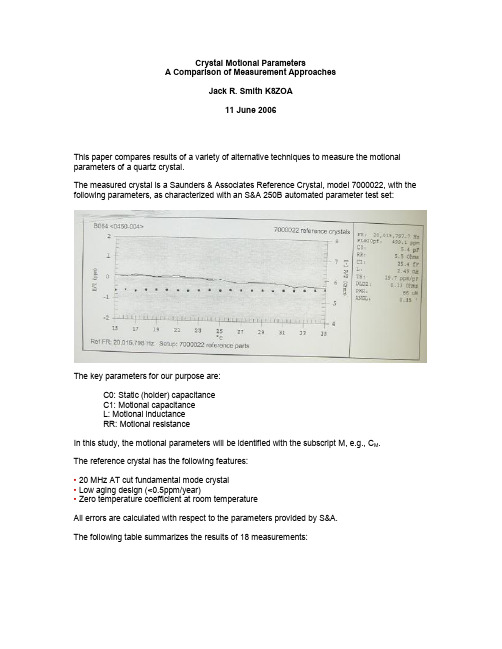
Crystal Motional ParametersA Comparison of Measurement ApproachesJack R. Smith K8ZOA11 June 2006This paper compares results of a variety of alternative techniques to measure the motional parameters of a quartz crystal.The measured crystal is a Saunders & Associates Reference Crystal, model 7000022, with the following parameters, as characterized with an S&A 250B automated parameter test set:The key parameters for our purpose are:C0: Static (holder) capacitanceC1: Motional capacitanceL: Motional inductanceRR: Motional resistanceIn this study, the motional parameters will be identified with the subscript M, e.g., C M.The reference crystal has the following features:• 20 MHz AT cut fundamental mode crystal• Low aging design (<0.5ppm/year)• Zero temperature coefficient at room temperatureAll errors are calculated with respect to the parameters provided by S&A.The following table summarizes the results of 18 measurements:MethodT e s t N u m b e rF i x t u r eM e t h o d o l o g yC o (p F )C 1 (f F )L 1 (m H )R 1 (o h m s )C 1 E r r o r %R 1 E r r o r % Saunders & Associates Calibration Standard0 N/A N/A 5.4 25.4 2.49 5.5 Std StdBoonton 250RX Meter C0 only @ 1 MHz 1 N/A N/A 5.52 G3UUR2 N/A 1 -- 24.73 2.65 -- -2.6% -- 09 Jun Pi Fixture & HP8752B 3 a 2 5.46 25.987 2.4336.77 2.3% 23.1%50 Ohm Transformer Fixture & HP8752B4 d 2 --28.91-- 6.5275 13.8% 18.7% Pi fixture SN-002 remeasure w/ HP8752B5 a 2 -- 26.446--6.392 4.1% 16.2%87510A with Fixture SN-001, 300 KHz Span, AUTO mode 6 a 5 -- 25.883 2.4475 6.6023 1.9% 20.0% 87510A with Fixture SN-001, 10 KHz span, power out: +20 dBm7 a 5 -- 26.463 2.3892 6.65 4.2% 20.9% 87510A with Fixture SN-001, 10 KHz span, power out: +10 dBm8 a 5 -- 26.468 2.3888 6.644 4.2% 20.8% 87510A with Fixture SN-001, 10 KHz span, power out: 0 dBm9 a 5 -- 26.4552.396.665 4.2% 21.2% 87510A with Fixture SN-001, 10 KHz span, power out: -10 dBm10 a 5 -- 26.479 2.3889 6.659 4.2% 21.1% Fixture SN-002, HP8752B, +/- 45 degree method 11 a 3 --26.26-- 6.659 3.4% 21.1% Remeasure 50 ohmtransformer fixture, HP8752B 12 d 3 -- 28.872 -- 3.72 13.7% -32.4% 12.5 Ohm Xfmr Fixture, HP8752B13b350.55--2.719 99.0% -50.6%50 ohm die-cast fixture, with 20 dB (in) & 6 dB pads (out), 0 dBm out of HP8752B, +/- 45 degree phase method 14 c 3 25.792 6.2916 1.5% 14.4%Same setup as 14, except measure fr & fs and calculate based on C0; shunting C only C0 and stray fixture15 c 3 -- 28.65 -- -- 12.8% --Same setup as 15, but with known 10.11 pF shunting capacitor16c3--28.50--5.83 12.2%5.9%HP8752B, 10 dB pad, Pi fixture sn-002, resistance via substitution method, Lm via Q measurement17 a 3 -- 26.152.426.18 2.9% 12.3% Resistance only via reflection, HP8752B18f66.82-- 24.1%Fixture a 12.5 ohm resistive pib 12.5 ohm transformerc 50 ohm - no transformerd 50 ohm transformere Reflection holderMethodology 1 G3UUR Oscillator frequency shift2 +/- 45 degree phase shift3 -3 dB bandwidth4 series and parallel resonance5 HP87510A Automatic characterization6 Reflection measurementThe methodologies and test fixtures are described in more detail later in this document.The following test equipment was used in these tests:HP8752B network analyzer, 300 KHz-3 GHz, with Minicircuits model UNMP-5075 75 ohm : 50 ohm matching padsHP87510A gain/phase analyzer, 100 KHz – 300 MHzMiscellaneous Minicircuit 50-ohm standards and pads, and miscellaneous adapters and cables. Boonton RX meter Type 250AHP 6205C DC power supplyHeath IM-2420 frequency counterBP Model DCM-601 digital capacitance meterHomebrew G3UUR oscillatorHomebrew test fixtures as described.Part I – Measurement Methodologies1. G3UUR Oscillator – Frequency Shift MethodThis method was developed by David Gordon-Smith, G3UUR, and popularized by Wes Hayward, W7ZOI. 1The above schematic shows the circuit I built. It follows the design of Reference 1, substituting2N4401s for the 2N3904s in the original design. I used Manhattan-style construction to build my unit.The procedure is to measure the frequency with the switch open and closed. When open, the crystal is in series with C2 and C0, the crystal’s holder capacitance.1 Hayward, Wes, Campbell, Rick, and Larkin, Bob, “Experimental Methods in RF Design,” (2003) American Radio Relay League, Hartford, CT at Page 3.19.To calculate the motional parameters, use the following equations:f fC C C S MD +=)(20MM C f L 2)2(1p =Cs should also include the strays associated with the switch and wiring. I measured Cs=34.1 pF in my oscillator. (To reduce stray capacitance, I used a two-pin header and shunt jumper instead of a standard switch.)C0 is the crystal holder capacitance.Δf is the shift in frequency between switch open and switch closedf is the frequency with switch closed.Remember to use proper units; capacitance is in farads (1pF = 10-12 Farads), f and Δf are in Hz, Lm is in Henries.Sample calculation with S&A calibrated crystal:Measured ParametersSwitch closed: 20016843 Hz Switch open: 20023109 Hz Δf = 6266 HzC0 = 5.52 pF = 5.52*10-12F (measured with Boonton model 250A RX meter at 1 MHz)Cs = 34.1 pF = 34.1*10-12F (measured with BP model DCM-601 digital capacitance meter)Calculated ParametersfF F C M 73.241073.24200168436266)101.341052.5(2151212=´=´´+´´=---mH H L M 56.21056.21073.24)200168432(13152=´=´´´´=--pA useful unit for motional capacitance is the femto farad, where 1000 fF = 1pF.We may compare the measured parameters with the calibration information:Parameter Measured Calibration Standard Error Cm 24.73 fF 25.4 fF -2.6% Lm 2.56 mH 2.49 mH +2.8% C0 5.52 pF 5.4 pF +2.2% Rm Not measured 5.5 ohms N/A2. Phase Shift MeasurementThe method recommended in international standards is to install the crystal in a low impedance test fixture, fed with an accurate, stable signal generator and measure the phase shift of the transmission signal near resonance.Historically, a stable signal generator and a vector voltmeter have been used to measure the phase of the transmission signal. In my case, I used either an HP8752B network analyzer, or an HP87510A gain/phase analyzer to generate the signal and measure the amplitude and phase of the transmission signal.Methodology and Equationsright shows theamplitude (toppanel) and phase(bottom panel) ofthe S&A calibrationcrystal in Fixture(a), the 12.5 ohmresistive pi designThe bottom tracehas markers at the+45 and –45 degreepoints.The +45 degreepoint is at –972 Hzbelow the zeroangle reference,whilst the –45degree point is1109 Hz above thezero reference.The ±45 degree bandwidth is thus 2081 Hz.We also use the same setup to measure Rm, by measuring the insertion loss at the zero phase point.When phase = 0 (marker 2), the insertion loss is 2.01131 dB.Note that the zero phase point is not the minimum loss point. In fact, the two are 89 Hz separated in this measurement.The relationship between attenuation and series resistance is:÷÷øöççèæ-=110220a L M R RWhereR M is the motional resistanceR L is the source and load resistance seen by the crystal (a function of the test fixture) α is the loss in dBApplying the measured data, we calculate R M :W =÷÷øöççèæ-´´=521.61105.122200131.2M RThe total resistance, R EFF , seen by the crystal is the sum of the load resistance (input and output) and the motional resistance, R M :R EFF = 2 R L + R M = 2 * 12.5 * 6.52 = 31.52 Ohms.The following formulas may be used to compute the motional parameters.)tan(2)(2J p J EFF R M R f f C ±D =)tan()(2J j p ±D =f R L EFFMThe standard calls for measurement at the ±45°, so φ = 45°WhereΔf is the frequency diffrerence between the ±45° points, measured at 2081 Hz. φ = 45°, so tan(45) = 1.R EFF = 31.52 ohms, as determined abovef R is the series resonant frequency , i.e., the frequency at which φ=0°.We now calculate the motional parameters:fF F C M 23.261023.26152.312001575722081152=´=´´´´=-pmH H L M 411.210411.212081252.313=´=´´´=-pWe now compare these measured values with the calibration standard:Parameter Measured Calibration Standard Error Cm 26.23 fF 25.4 fF +3.3% Lm 2.411 mH 2.49 mH -3.2% C0 Not measured 5.4 pF Rm 6.52 5.5 ohms +18.5%3. -3 dB Bandwidth MethodMeasuring the ±45°bandwidth requires equipment not easily available to all experimenters.2It’s also possible to derive motional parameters from a 3 dB bandwidth measurement. This may be made with much simpler equipment.The figure at the right shows the -3dB bandwidth data for thecalibration crystal. The crystal isinstalled in the type (a) 12.5 ohmresistive pi fixture.The network analyzer calculates the 3 dB bandwidth as 2056 Hz, and the measured Q as9737.5,with a center frequency of 20.015627 MHz. The attenuation at the point of minimum loss is 1.9733 dB.We base the motional parameter calculation on the definition of Q:EFFMr dB R R L f f f Q p 23=D =-Solving for L M we find:REFFM f QR L p 2=WhereR EFF is the effective series resistance seen by the crystal, R M + 2 * R L .f R is the series resonant frequency, i.e., the frequency of minimum loss, 20.015627 MHz. Δf is the –3dB bandwidth, displayed as 2056 Hz.Q is the ratio of f R to the –3dB bandwidth, displayed as 9737.5 (or can be calculated as 20015627 / 2056 = 9735)2See K8IQY’s low-cost approach to 3 dB crystal parameter measurements at /testequipment/pvxo/pvxopage.htm and/testequipment/pvxo/Atlanticon2002V1R5.pdf .MR M L f C 2241p =Using the methodology described before, we calculate R M and R EFF using the measured 1.9733 dB loss at the center frequency.R M = 6.38 ohms, REFF = 31.38 ohms.Calculating L M :mH H L M 429.210429.210015627.20238.315.973736=´=´´´´=-pfF F C M 03.261003.2610429.2200156274115322=´=´´´´=--pWe now compare these measured values with the calibration standard:Parameter Measured Calibration Standard Error Cm 26.03 fF 25.4 fF +2.5% Lm 2.429 mH 2.49 mH -2.4% C0 Not measured 5.4 pF Rm 6.38 5.5 ohms +16.0%4. Series and Parallel Resonant FrequenciesA variant on the two frequency method used in the G3UUR oscillator is to measure the series andparallel resonant frequencies of the crystal, and from their ratio determine the motional parameters.The figure at the right shows the series f S (at marker 1) and parallel f P (marker 2) resonantfrequencies of the calibrated crystal.The precise frequencies measured are:The relationship between motional parameters and the series and parallel resonant frequencies is:)(210STRAY S P M C C f f C +÷÷øöççèæ-=MR M C f L 2241p =Wheref P and f S are the parallel and series resonant frequencies as described above C0 is the holder capacitanceC STRAY is the stray shunting capacitance of the test fixtureTo measure C STRAY , we determine the attenuation through the test fixture with the crystal removed.Assuming that the stray capacitance is small, we can use the attenuation to determine thecorresponding capacitive reactance and from that the value of Cstray.With the crystal removed, the attenuation has a mean value of 44.3 dB at 20.03 MHz.This corresponds to a capacitive reactance of 4.08 K ohm,corresponding to1.95 pF stray capacitance shunting the crystal socket.As previouslymentioned, measuring the calibrated crystal at 1.0 MHz with a Boonton 250 RXmeter showed the C0 = 5.61 pF.Hence, C0 + C STRAY = 5.52 + 1.95 pF = 7.47 pF.We now are in a position to calculate the motional parameters:fF pF C M 63.2447.7212001562520048625=´´÷øöçèæ-=mH L M 57.21063.2420015625411522=´´´´=-pWe now compare these measured values with the calibration standard:Parameter Measured Calibration Standard Error Cm 24.63 fF 25.4 fF -3.0% Lm 2.57 mH 2.49 mH +3.2% C0 5.61 5.4 pF +3.9% Rm 6.35 5.5 ohms +15.4%(Rm is computed from the marker 1 attenuation value of 1,9649 dB)measuring theseries andparallelresonantfrequencies, besure you don’tinadvertentlymeasure aspuriousresonance, asmost crystalsexhibit severalspuriousresonancepoints abovethe true parallelresonancepoint.The calibrated crystal, for example, shows two major and one minor spurious resonance points.5. HP87510A Automatic characterizationThe HP87510A gain/phase analyzer has an internal firmware crystalresonator characterization routine that computes and displays a six-parameter model. To use theautomatic characterization function, the crystal must be installed in a transmission fixture.The primary advantage of the87510A’s automatic characterization function is that its analysis is based upon curve fitted data involving at least 8 measurement points. It thusoffers the prospect of increased accuracy by leveraging multiple data points.The 87510A’s Operation Manual describes the methodology used to calculate the six parameter values:1. Obtains the admittance characteristic circle diagram2. Obtains the maximum conductance (G max )3. Obtains frequencies f 1 and f 2 (f 1<f 2) of two points where conductance is half the maximumconductance. 4. Calculate f s by 21f f f s ´=5. Obtains susceptance B fs at f s6. Calculate ωS by S S f 2p w =7. Assumes that the frequency at which the phase difference becomes 0° near the parallelresonance frequency is f a and obtains its conductance G a . 8. Calculate ωa by a a f 2p w =9. Assumes that the frequency at which the phase difference becomes 0° near the seriesresonance frequency is f r .10. Calculates the constants using the above values and the following equations:12f f f Q SS -=SB BC w 221'0+=max 1G Q L S Sw =max 0'01G C C R =S S Q G C w max1= 1max01R G R -=SfsB C w =2210202101C R R C R G G a a a w w +-=Applying these equations by pressing the 87510A’s appropriate soft key produced the followingmotional parameters and errors:Parameter Measured Calibration Standard Error Cm 25.883 fF 25.4 fF +1.9% Lm 2.4475 mH 2.49 mH -1.7% C0 N/A 5.4 pF Rm 6.60 5.5 ohms +20.0%The measured parameters are sensitive to the span used and the above data represents the best case. Other 87510A measurements are summarized in the measurement table and display errors up to 4.2%.6. Reflection Resistance MeasurementThe final measurement approach was an attempt to resolve the wide gap between the reference crystal’s stated motional resistance of 5.5 ohms, whilst all my measurements were in the range 6.3 to 6.8 ohms, with 6.6 ohms being the most common value.In this mode, the network analyzer is successively calibrated, at the reflection measurement port, with an open, short and load (50 ohm) standard. The unknown is attached to the reflection measurement port and the instrument set to internally convert the complex reflection coefficient to either Z/theta or R and jX values.The data confirms the transmission-mode values in the 6.5 ohm range. At the point where the imaginary (reactive) part of the impedance is zero, the real (resistive) value is 6.8 ohms.Somecrystalsexhibitsignificantchange inmotionalresistanceas drivelevelchanges.To test thisas apossiblereason forthe consistent divergence between measured and calibration motional resistance, I ran a power sweep test using the HP87510A gain/phase analyzer.As shown, over the range -50 dBm to +20 dBm, R M changes less than 0.04 ohms and stays in the 6.6 ohm range.The crystal is held in a (a) type resistive fixture, with 10 dB attenuation between the 87510A’s output and the fixture.The extra attenuation, plus the fixture’s loss, means that the power delivered to the crystal is much less than the 87510A’s output shown on the horizontal axis. +20 dBm corresponds to approximately 4 mA crystal current, or about 100 microwatts.Marker 1, at +19.26 dBm corresponds to 88 microwatts, the power level at which the calibrated crystal was tested by S&A. The measured value at this point is 6.62 ohms.To verify the accuracyof the power sweepand test fixture, Isubstituted a 1% 10ohm, 1206 surfacemount resistor for thetest crystal.Although there issome variation, the87510A results arequite close to the testresistor’s 10.0 ohmmarket value.At DC, a four-wiremeasurement showsthe test resistor is10.03 ohms.Part II – Test FixturesI built and used five test fixtures:(a) Resistive Pi Fixture:The resistive pi fixture matches the 50 ohm input and output to 12.5 ohms. The ones I built follow the standard design in IEC standard, except that the phase compensation trimmers across the 14.3 ohm resistors are not used and I used the nearest 1% standard resistor values.The photo to the right shows the prototype pad unit I built, using Manhattan-style construction. The pad is constructed with re 1%, 1206 size surface mount resistors.It’s important to shield the input and output ports.The three photos show the printed circuit version of the prototype.The resistors provide a reasonably good impedance match and hence external stabilizing pads are less necessary than for other fixtures.(b) Transformer Pi FixtureIn addition to a resistive pad matching approach, it’s possible to use a 2:1 winding transformer to provide a 50ohm to 12.5 ohm impedance transformation.My transformer fixture uses two Coilcraft WB1040transformers. The transformers have a bandwidthof 200 KHz – 300 MHz.Any error in impedance on the 50 ohm side will bereflected in errors in the 12.5 ohm transformedside, so stabilizing pads will normally be employedon both sides of the fixture.(c) 50 Ohms, no Matching, no LossThe simplest fixture simply breaks theconnection between signal generatorand receiver and inserts the crystal.I built one into a Hammond die-castbox and brought the connections out tobinding posts.In order to accurately compute the crystal motionalparameters, it’s important that the impedance seen bythe crystal be accurately known. With a simple fixtureof this type, it’s important to use pads on both the inputand output in order to provide accurate and stable impedance.(d) 50 Ohm Transformer FixtureI also built a variant of the 12.5 ohmtransformer fixture described at (b),but with Coilcraft model WB1010transformers providing a 1:1impedance ratio.It is otherwise identical with the fixturediscussed in section (a). This fixture isalso to be used only with a controlledimpedance environment, as thetransformers reflect actual input andoutput impedance.(e) Reflection Test Fixturevia reflection, the reference crystal wasTo measure Rattached to the 8752B network analyzer using a standard BNC-to-binding post adapter, HP model 10110A.。

新型一维三元光子晶体滤波器设计佟悦;胥馨【摘要】This paper discussed a new type of one-dimensional three yuan photonic crystal filter,which breaking through the traditional filter only control the characteristics of the forbidden band.The most difference of the new type filter and the traditional filter,that was not to control the forbidden band,but to control the conduction band,that was the filter can control some useful light through the filter.%本文突破传统的滤波器只控制禁带的特点,研究了一种新型的一维三元光子晶体滤波器.这种滤波器与传统滤波器最大的区别在于它不是禁止某些无用的光通过滤波器,而是要控制某些有用的光透过滤波器.【期刊名称】《吉林师范大学学报(自然科学版)》【年(卷),期】2011(032)004【总页数】3页(P80-82)【关键词】光子晶体;禁带;滤波器【作者】佟悦;胥馨【作者单位】空军航空大学基础部,吉林长春130022;空军航空大学基础部,吉林长春130022【正文语种】中文【中图分类】O436半导体的应用,如手机、计算机、录音机等,对人类的生产和生活影响十分深远.但在其发展中也出现了一些问题,比如集成电路能量损耗大,易发热,集成器件延迟速度不能达到现在信息高速时代的要求等.为了解决这些问题,人们找到了一种新型材料,就是“光子晶体”.光子晶体本身的特性完全能够弥补半导体的不足.对于一维光子晶体滤波器的研究已经很深入了,通常人们还是以阻止某些光通过晶体为目的来进行研究的.为了突破前人,以达到更加优化滤波器的目的,本文设计了一种新型一维三元光子晶体滤波器.一维三元光子晶体就是三种介质在一个方向上周期性的交替排列,而在垂直于该方向的平面上为均匀介质的结构.图1为一维三元光子晶体示意图.图2为一维二元、三元光子晶体的透射谱的比较.从图中可以看出,三元光子晶体的中心禁带宽度比二元光子晶体的要宽,并且在短波区出现了二元光子晶体所没有的禁带,这使三元光子晶体产生了更大的实用价值.传统滤波器的设计理念是使三层介质的光学厚度取值分别为:通过改变 u和v的取值、介质折射率、晶体周期等方法来达到使某些光不能通过晶体的目的.本文旨在突破传统的设计理念,目标不在控制禁带,而是如何才能有效的控制导带,也就是控制何种光通过晶体.以此为目的,所做的设计如下.以折射率为4.10(碲化铅)、3.23(砷化镓)和1.45(二氧化硅)的三种物质组成的一维三元光子晶体为例,单块晶体周期为20,中心波长为1000纳米.三层介质的光学厚度取值分别为这样的晶体的透射谱与传统滤波器投射谱存在很大差别,如图3所示.上图为传统滤波器透射谱,下图为新型滤波器透射谱,从图中可看出,禁带区和导带区几乎完全相反,并且禁带变宽,导带也变宽,位置移动.这样我们就可以通过控制导带的边缘来控制透光范围.从图中可以看出,中心波长处在导带区,并且导带的左右边缘以及禁带都是是关于中心波长对称的.通过这一点,就可以用根据已知的波长范围求出中心波长,进而求出透带宽度:d=通过计算,画出透带宽度与N的关系图图5.从图5可以知道,当给定了透过波的范围,就可以确定N的值,从而就可以找出最合适的三种物质组成光子晶体.以可见光为例,让橙、黄、绿、青四种颜色的光通过晶体.此四种光的波长范围为450~630纳米.通过计算可得中心波长为525纳米,标度化的透带宽度为0.3333,N=8.5438.组成晶体的三种物质的最佳组合为1.35(冰晶石),1.4584(二氧化硅),4.10(碲化铅).得到的透射谱为图6.从图中可以看出,在450~630纳米波段为导带区,这与设想完全一致.本文突破传统的滤波器只控制禁带的特点,研究了一种新型的一维三元光子晶体滤波器.新型的滤波器是以改变物质的光学厚度为出发点,从而得到了与以往的研究完全不同的结果.这种滤波器与传统滤波器最大的区别在于,它不是禁止某些无用的光通过滤波器,而是要控制某些有用的光透过滤波器.这种以控制导带为特色的新型滤波器,应用前景十分广阔.【相关文献】[1]E.Yabonovitch.Inhibited Spontaneous Emission in Solid-State Physics and Electronics[J].Phy.Rev.Lett.,1987,58(20):2059~2062.[2]S.John.Strong Localization of Photons in Certain Disordered Dielectric Superlattices[J].Phys.Rev.Lett.,1987,58(23):2486~2489.[3]张道中.光子晶体[J].物理,1994,23(3):141~147.[4]Sozuer H,Haus J,Inguva R.Photonic bands:convergence problems with the plane-wave method[J].Phys.Rev.B,1992,45:13962~13972.[5]A.Van.Blaaderen.Materials science-Opals in a new light[J].Science,1988,282(5390):887~888.。


晶体滤波器设计范文晶体滤波器(crystal filter)是一种频率选择性滤波器,利用晶体的特性来实现滤波的功能。
在无线通信领域,晶体滤波器被广泛应用于无线电收发器以实现信号的滤波和频率选择。
本文将介绍晶体滤波器的设计过程,包括滤波器的原理、设计要求和设计步骤。
一、晶体滤波器的原理1.谐振频率:晶体在特定频率下具有谐振的特性,称为晶体的谐振频率。
利用晶体的谐振频率可以实现对信号的选择性传递。
2.谐振电路:晶体谐振电路是用来实现谐振频率的选择性传递,一般由电容和电感组成。
在谐振频率附近,电感和电容共同作用形成谐振回路,具有高阻抗,从而起到滤波的效果。
3.并联谐振电路和串联谐振电路:晶体滤波器可以通过并联谐振电路和串联谐振电路实现信号的选择性传递。
并联谐振电路类似于谐振回路并联的模式,它对输入信号进行选择性地短路,实现对一些频率范围内的信号的传递。
串联谐振电路类似于谐振回路串联的模式,它对输入信号进行选择性地阻断,实现对一些频率范围外的信号的抑制。
二、晶体滤波器的设计要求在设计晶体滤波器时,需要考虑以下几个要求:1.频率选择性:晶体滤波器应能够选择性地传递特定频率范围的信号,同时抑制其他频率的信号。
2.抑制带宽:晶体滤波器在设计过程中应确定一个带宽范围,即传递范围内的信号被传递,超出范围的信号被抑制。
3.插入损耗:晶体滤波器应尽量减小信号传递过程中的能量损耗,以提高传输效率。
4.通带和阻带衰减:晶体滤波器应能够对输入信号的通带内和阻带外的信号进行衰减,以实现滤波功能。
5.相位响应:晶体滤波器设计中需考虑信号的相位延迟,以确保输出信号的准确性。
三、晶体滤波器的设计步骤在设计晶体滤波器时,可以遵循以下步骤进行:1.确定设计频率范围:根据实际应用的要求,确定晶体滤波器的设计频率范围。
2.选择晶体材料:根据设计频率范围,选择合适的晶体材料,通常有石英、石英晶体和陶瓷晶体等。
3.计算并选择电容和电感:根据晶体材料的参数和设计频率,计算并选择合适的电容和电感值,以满足设计要求。
晶体滤波器crystal filte用晶体谐振器组成的滤波器。
与LC 谐振回路构成的滤波器相比,晶体滤波器在频率选择性、频率稳定性、过渡带陡度和插入损耗等方面都优越得多,已广泛用于通信、导航、测量等电子设备。
1921 年W. G.凯地将晶体谐振器用于各种调谐电路,形成了晶体滤波器的雏形。
1927年L.艾斯本希德把晶体谐振器用于真正的滤波电路。
1931年W.P.梅森又把它用于格型滤波器。
60年代中期,集成式晶体滤波器研制成功,晶体滤波器在小型化方面有了很大发展。
石英晶体滤波器是采用石英晶体谐振器为基本元件的电气滤波器,由于它有很高的品质因数(数万以上),因此在军、民用电子设备中应用极其广泛,特别是在中频范畴内具有不可替代的地位。
石英晶体滤波器可分为低通、高通、带通和带阻晶体滤波器。
其中又以带通及带阻晶体滤波器最为常用。
各种晶体滤波器都可由梯型或差接桥型电路组成,而差接桥型电路具有所需元件较少、对元件参数要求较低、设计灵活,因此在大多数工程设计中,通常采用这种电路。
石英晶体滤波器具有以下特点:阻带衰减高:石英晶体滤波器具有陡峭的阻带衰减特性,一般阻带衰减都在60dB以上,有的甚至达到90dB以上。
矩形系数好:石英晶体滤波器的矩形系数一般在2到5左右,频率较低的可达到1.8左右,具有良好频率择性。
频率温度稳定性好:由于石英晶体在宽温度范围内具有的特性,使得晶体滤波器的幅频特性在宽温度范围内具有非常高的稳定性。
体积小:石英晶体滤波器所需的元件较少,而且许多元件都可实现表贴化,因此,这种晶体滤波器的体积相对较小。
插损小:一般均小于5dB。
石英晶体谐振器是最常用的晶体谐振器之一,它在滤波器中主要用作窄带通滤波器。
钽酸锂或铌酸锂晶体谐振器的耦合系数和频率常数较大,适用于制做高频宽带通滤波器。
其他压电材料因温度稳定性较差,很少采用。
当作用于晶体谐振器的电信号频率等于晶体的固有频率时,电能通过晶体的逆压电效应在晶体中引起机械谐振产生机械能;在输出端,正压电效应又将这种机械能转换为电信号。
光子晶体光纤滤波器的设计与性能研究光子晶体光纤滤波器,在光通信领域发挥着重要的作用。
它的设计和性能研究,对于提高光纤通信系统的传输性能、减少光耦合损耗、增强光学信号处理能力等方面具有重要的意义。
一、光子晶体光纤滤波器的基础原理光子晶体光纤滤波器是一种基于光子晶体结构的光学器件。
光子晶体是一种具有周期性介电常数分布的材料,它可以通过调节介电常数的大小、周期和结构等来调控光子能量的传输和分布。
光子晶体光纤滤波器的基本原理就是利用光子晶体的调控作用,实现光的波长选择性传输和过滤。
光子晶体光纤滤波器的核心组成部分是一段光子晶体光纤。
光子晶体光纤是一种由光子晶体结构组成的光纤。
它具有周期性的介电常数分布结构,可以在一定范围内选择性地引导光子能量的传输和分布。
在光子晶体光纤中,由于光的能量被限制在周期性的介电常数分布结构中,光的能量密度被高度局限,从而可以实现波长选择性的过滤和传输。
二、光子晶体光纤滤波器的设计光子晶体光纤滤波器的设计需要考虑多种因素,如光子晶体结构、波长范围、滤波特性等。
其中,光子晶体结构的设计是关键因素之一。
光子晶体结构分为一维、二维和三维结构。
一维光子晶体结构是由一层介电常数周期性分布的材料组成的,常用于简单的滤波器和波长选择器中。
二维和三维光子晶体结构则更加复杂,能够实现更高级别的光学控制和加工。
在设计光子晶体光纤滤波器时,需要考虑具体应用场景和实现效果,选择合适的光子晶体结构。
同时,在滤波器的设计中,还需要考虑光子晶体光纤的长度、直径、折射率、波导长度等多种参数。
这些参数也会影响到滤波性能和传输特性。
三、光子晶体光纤滤波器的性能研究光子晶体光纤滤波器的性能研究是对其设计的验证和完善,也是对其实际应用的考验。
常见的光子晶体光纤滤波器性能指标包括传输特性、滤波特性、波长调谐范围、插入损耗等。
其中,传输特性是指光子晶体光纤滤波器对不同波长光的传输情况。
不同波长光在光子晶体光纤中的传输特性是不同的,因此需要研究滤波器在不同光波长下的传输性能。
晶体滤波器设计
图5.1-9 几种切型的频率温度特性曲线由图可知AT切型在-55~+85度之间频率变化都很小,特别是在-20~+40度范围内,频率基本上与温度无关。
2、石英谐振器等交电路
及电抗频率特性(1)石英谐振器等效电路模拟晶体谐振点附近情况,它相当于一个串联谐振电路,因此可用集中参数LS、CS、RS来等效,LS称之动态电感,CS称之动态电容,RS称之动态电阻,其基频等效电路见图5.1-10图5.1-10
石英谐振器基频等效电路图中右边支路的电容C0称为石英谐振器的静电容。
它是以石英为介质在两极板间形成的电容,其容量主要决定于石英片尺寸和电极面积,可用下式表示;式中E为石英的介电常数;S为极板面积;D为石英片厚度。
C0一般在几皮法到几十皮法之间。
石英晶体的Q值非常高,是一般LC振荡回路远所不及,Q值与动态参数关系为目前广泛使用的AT切型密封谐振器Q值,一般为(50~300)*10的3次方,而精密型的Q值可达(1~5)*10的8次方。
(2)石英谐振器等效电路电抗频率特性由等效电路可知,有两
个谐振角频率,一为左支路的串联谐振角频率WS,即石英片本身自然角频率另一石英谐振器的并联谐振角频率当忽
略动态电阻RS的影响时,由石英晶体和等效电路可求其效电抗X。
其电抗频率特性曲线示于图5.1-11。
图5.1-11 石
英谐振器电抗频率特性由图5.1-11可见当W大于WPW、W小于WS时电抗JX为容性;当W在WS、WP之间时,电抗JX为感性。
石英晶体滤波器工作时,石英晶体两个谐振频率之间的宽度,通常决定滤波器的通带宽度。
为要加宽滤波器的通带宽度,则必须加宽石英晶体两谐振频率之间的宽度,这通常可用外加电感与石英晶体串联或并联的方法来实现。
表5.1-8示出部分石英晶体的主要性能。
差接桥型带通晶体滤波器设计晶体滤波器也有两种方法:一是影象参数法;另一是有效参数法(即综合法)。
综合法是目前广泛采用的有效方法。
在许多现代电子设备中应用最多的是带通晶体滤波器,按其频带分类有察窄带、中等带宽、宽带三类,其相对带宽分别为小于0.1%以下、0.1%~1%和大于1%。
带通晶体滤波器中,以差接桥型或称之格型应用最为普遍,差接桥型电路实际上是惠斯登电桥电路。
其典型形式有以下两种:1、窄带差接桥型带通晶体滤波器此种滤波器的零件参数是由网络综合法设计计算得出的。
先将全极点归一化低通LC梯型电路转换成带通梯型电路,然后再由巴尔特勒特中剖定理,将梯型电路变换差接型电路或桥型电路或桥型电路,并用晶体谐振器等效来实现。
窄带差接桥型带通晶体滤波器电路的设计请参阅文献(7)。
2、宽带差接桥型带通晶体滤波器的设计表5.1-9列出了个设计公式和例子。
晶体滤波器定型产品的选用目前,国内外都已经生产出具有一定
技术指标的晶体滤波器系列产品。
现只介绍我国某著名厂家的两大类型产品如下。
1、通用型晶体滤波器表5.1-11示出通用型晶体滤波器主要性能参数。
2、单片晶体滤波器在单片晶体滤波器中又以集成式单片晶体滤波器性能为佳,它和普通分立式晶体滤波器相比,有更多优点:体积小,温度稳定性和机械稳定性都好,生产周期短,成本低,适合大批量生产。
自60年代集成晶体滤波器问世以来,世界各国竟先研制,取得很大发展。
直到目前,频率范围从3MHZ到180MHZ,相对带宽在0.002%~0.35%之间单片晶体滤波器已得到了广泛应用,低于5MHZ和高达35.0MHZ的集成式单片晶体滤波器早已研制成功。
集成式单片晶体滤波器主要用于通信系统之外,一般的测量和综合也广泛应用,用来提纯频谱、消除寄生信号和混杂的谐波成分等。
55.1-12列出部分单片晶体滤波器主要性能参数。