飞思卡尔 HCS12 微控制器 ECT PWM 中文版
- 格式:pdf
- 大小:952.52 KB
- 文档页数:46
9S12 系列单片机的ECT (Enhanced Capture Timer Module)模块是在原68HC12 的 Standard Timer module 基础上加以增强功能形成的。
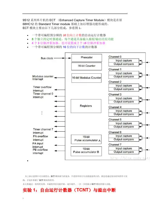
ECT 模块主要由以下几部分组成,参看图1:•一个带可编程预分频的16位向上计数的自由运行计数器•8个独立的定时器通道,每个通道具备输入捕捉/输出比较功能•4个8位脉冲累加器,也可设置成2个16位脉冲累加器•一个带可编程预分频的16位的向下计数的计数器•从上面示意图中可以就看出,ECT 模块相当的复杂,不是简单的几句话就能说明白的。
我也是通过很长时间的学习实践,才逐步掌握了ECT模块的使用。
本文将通过一系列的实例,从最简单的功能开始,逐步展开。
一步一步的展示ECT 模块的强大功能。
实验1:自由运行计数器(TCNT)与溢出中断自由运行计数器(TCNT)也称为自由运行主定时器,是一个16位的计数器,可以说是ECT的核心。
在系统复位时,这个自由运行计数器的初值为$0000。
当ECT 模块运行时,自由运行计数器从$0000~$FFFF 循环递增计数。
当计数器溢出复零时,会置位中断标志。
利用这个计数器,可以产生一个周期的中断信号。
TCNT 的输入时钟也是可以选择的,图2 给出了TCNT 的时钟源的示意图。
可以看出,TCNT的输入时钟可以来源于总线时钟、总线时钟经过预分频、外部引脚输入的脉冲、外部引脚输入脉冲经过脉冲累加器分频这四种选择。
当然,选择哪个时钟源其实就是在程序中设置一下相应的寄存器这么简单。
了解了上面的介绍,就可以开始本文的第一个例子了,这个例子非常简单,将BUS CLOCK 分频后作为TCNT 的输入时钟,使能TCNT 溢出中断。
在开始代码之前,还需要介绍几个程序中用到的寄存器。
TCNT寄存器(Timer Count Register)这个寄存器其实已经介绍过了,它是一个16 位的只读寄存器。
在每个时钟输入下计数值会自动加1,当计数值为0xFFFF 后下一个时钟脉冲会使计数器溢出为0x0000。
中文译文第1章器件概述S12XS-系列1.1简介新S12XS家族16位微控制器是S12XE家族的兼容,简化版本。
这些家庭提供了一种简单的方法来制定共同的平台,从低端到高端应用程序,最大限度地减少软件和硬件的重新设计。
针对通用汽车的应用和CAN节点,这些应用的一些典型的例子分别是:车身控制器,乘员检测,车门模块,RKE接收器,智能执行器,照明模块和智能接线盒以及很多其他。
该S12XS家族保留了许多S12XE家族包括纠错码的功能(ECC)的快闪记忆体,一个独立的数据闪存模块的代码或数据的存储,一个调频锁相环(IPLL),提高了EMC性能和快速的ATD转换器S12XS家族将提供32位的性能与16位MCU的所有优势和效率。
它将保留低成本,目前享有的功耗,EMCand代码大小效率优势由飞思卡尔现有的16位S12和S12X MCU系列的用户。
像其他S12X成员家庭,S12XS家庭将运行16 - bit宽访问无需等待状态的所有外设和回忆。
该S12XS家庭将可在112引脚LQFP ,80引脚QFP ,64引脚LQFP封装选项和保持与S12XE家族针兼容性的高水平。
除了在现有的I / O端口每个模块,多达18个进一步的I / O端口,可与中断功能,允许唤醒从停止或等待模式。
外设集包括MSCAN ,SPI,2个SCI,可,一个8通道24位周期中断定时器,8 - 通道的16位定时器,8通道PWM和多达16 - 通道12位ATD转换器。
软件控制外设到端口的路由可以访问外设模块的灵活组合在较低的引脚数封装选项。
1.1.1特点在S12XS-系列的特性都在这里列出。
请参阅表D-1对于内存选项和表D-2外设功能,可在不同的家庭成员。
•16位CPU12X- 向上与S12指令集除了五个模糊的指令兼容(MEM,W A V,W A VR,REV,REVW),它已被删除-增强的变址寻址-- 访问大数据段独立PPAGE的-•INT(中断模块)-- 七个级别的嵌套中断-- 中断源到每个灵活分配中断级。
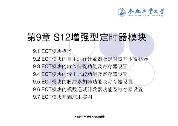
第9章S12增强型定时器模块
9.1 ECT模块概述
9.2 ECT模块的自由运行计数器及定时器基本寄存器
9.3 ECT模块的输入捕捉功能及寄存器设置
9.4 ECT模块的输出比较功能及寄存器设置
9.5 ECT模块的脉冲累加器功能及寄存器设置
9.6 ECT模块的模数递减计数器功能及寄存器设置
9.7 ECT模块基础应用实例
定时器模块的中断源名称、所对应的中断标志寄存器中的中
随着下一
,
表9.7 边沿检测器电路设置
ICSYS)
定时器中断允许寄存器(Timer Interrupt Enable Register,TIE)
该动作或事件与自由运行计
位比较器开
强行参与管理通
比较结果输出动作设置
中的对应位将被传送到定时器端口数据
相关联,,相关联
的计数脉冲分
上出现的信号有效边沿将使主定时器中断标志寄存
锁存方式和队列方式。
锁存方式和队列方式
表9.11 时钟选择
(16-Bit Pulse Accumulator B Control Register,
,
2(Pulse Accumulators Count Registers 3 and 2,
0(Pulse Accumulators Count Registers 1 and 0,位脉冲累加器PAC1和PAC0串联形成16位脉冲累加器PACB。
当PACB允许。
STC12内部PWM使用方法解析首先说一下PWM是一个什么样的东西,PWM的中文名字叫做“脉宽调制”,也就是说呢,我们的电路有两种状态,通或者不通,我们用单片机控制输出高电平低电平从而控制电路的通断来达到我们想要的某种模拟电路特有的效果的一种技术。
我们举个例子,比如说我们的直流电机直接接在五伏的电源上,要么全速运转,要么不转。
那我们怎样实现调速呢?我们可以通过单片机来控制这个电路,让电机电路通一段时间断一段时间。
比如说通一秒断一秒,那么电机的速度就会比全速运转时候低,不断改变这个通断之间的间隔时间,我们就可以达到一种调速的效果。
下面呢,我们就切入正题。
STC12C5A60S2这款单片机(下面说成12系列单片机),与89系列的单片机相比,它的内部增加了独立的PCA(计数器阵列,说简单点就是好几个计数器)或者说PWM模块,通过配置相关的特殊功能寄存器,我们可以实现一些额外的功能,比如说计时器,高脉冲输出,PWM输出等,如果我们用这种方法来实现PWM功能,要比用定时器加中断组合那种方法简单很多。
大家可能都看过那个技术文档,但是不得不说它的技术文档写的真是让人不敢恭维。
经过查阅资料,还有逛论坛,我大致了解了PCA模块,它到底是什么样一个东西,应当怎样用等。
下面我把相关的内容分享给大家,与大家交流一下。
如果有什么不对的地方,大家可以评论里边指出来,一定虚心思考。
我们看官方对PCA模块的介绍:对于图片里边提到的定时器的概念,大家已经非常熟悉了,而“捕获/比较器”,这个东西对我们来说可能比较生疏,其实通俗的说呢,在PWM功能里边,模块0与模块1里边的捕获比较器,就是一个比较大小的硬件装置。
假如有一个固定的值装在模块0的特殊功能寄存器里边,有一个外部来的外来值与它里边装的那个值不停的进行比较大小这种操作,如果外来的值比较小,那么这个比较大小的装置就会输出0,反之输出1。
(至于捕获模式,我们暂时用不到,他们其实是一个可以检测到相应引脚高低电平变化的硬件装置,我们知道,引脚拉高拉低并不是一下子就完成的,无论拉高或拉低,都有一定的上升或下降沿,捕获其实捕获的就是这种上升下降沿,一旦捕获到,可以触发相应的中断,这些都由软件决定。
MC9S12DG128实验使用手册目录第一章概述 (2)第二章硬件电路原理 (4)2.1子板硬件原理 (4)2.1.1、MCU引脚接口部分 (5)2.1.2、串口通信部分 (6)2.1.3、电源部分 (6)2.1.4、复位电路部分 (6)2.1.5、I/O端口电路部分 (7)2.1.6、晶振电路与BDM插头部分 (7)2.2母板硬件原理 (8)2.2.1、电源部分 (9)2.2.2、MC9S12DG128开发板与各接口部分 (9)2.2.3、串口通信部分 (11)2.2.4、LED数码管显示部分 (12)2.2.5、8位数字量输入输出部分 (13)2.2.6、红外发射接收部分 (15)2.2.7、LCD显示部分 (15)2.2.8、模拟量输入部分 (15)2.2.9、蜂鸣器和喇叭部分 (15)2.2.10、键盘输入部分 (16)2.2.11、继电器部分 (16)2.2.12、打印机部分 (17)2.2.13、CAN总线部分 (17)第三章MC9S12DG128教学平台快速入门 (18)3.1硬件连接 (18)3.2软件应用 (20)第一章概述天津工业大学Freescale MCU/DSP研发中心开发的DG128实验系统,其功能基本上和美国MCUSLK系统相同,而且根据中国的教学情况重新设计了一些功能、力求达到更好的实验效果。
DG128实验系统由主板和独立的MCU子板构成。
DG128实验系统的主板插槽和美国的MCUSLK系统相互兼容,主板的插槽可以插包括S12、S08、 HC08各系列MCU子板。
MCU子板可以单独调试运行,也可以插在主板上调试,充分利用主板丰富的硬件资源。
MC9S12DG128具有16位中央处理器(HCS12 CPU)、128KB Flash EEPROM、8KB RAM、2KB EEPROM,以及定时器通道、键盘中断和A/D通道等接口。
MC9S12DG128实验系统可以直接与CodeWarrior相连,具有下载程序、在线单步运行、断点调试、连续运行、修改寄存器和存储单元等特点,可以很方便的进行教学。
中文2075字外文资料原文Design and Implement of Responder Based on Freescale HCS12Single Chip MicrocomputerResponder is also known as the first signal discriminator, which is widely used in various competitions. It can judge the number of the first player accurately, fairly and intuitively. Currently, a variety of quiz responder has emerged on the market, in which a small responder is commonly designed with small-scale digital integrated circuit. Although the technology has been quite mature,but it is simple function, low intelligence, high fault, simple display, less flexibility, not convenience for upgrade, it has been unable to meet all kinds of requirements for intellectual competitions and variety shows. Therefore, it is necessary to develop some kinds of responder which are more suitable for applications.In recent years, with the rapid development of science and technology, the applications of single-chip microcomputer are becoming widely, which promotes the development of traditional measurement and control technology. In this paper, Freescale HCS12 [1-3] is designed as a core component to achieve an intelligent digital responder with 8-channel [4-8], it has some breakthroughs on technology, function and other aspects, comparing with the past responder. It is characterized by simple structure, powerful, good reliability, practicability, so that the competition can really carried out on just, fair and open rules.The basic functions of responder designed in this paper are:(1) The system can limit the competition time and answer time of the alarm;(2) The system can identify the answer signal and identify the player's number;(3) The system can calculate score for each player and display the scores.Responder can accommodate 8 players numbered 1 to 8. In addition, LED digital tubes are designed to display the latched data. After race host clears the system, if participants press switch, and after answer is certificated whether it is correct or not, the number of first player to answer in action is immediately shown by digital tubes. Responder should have a strong ability to distinguish players to answer in the action, its resolution reaches at least a few ms After the requirements and functions of responder are analyzed, the following circuits are required in general:1、Responder circuitThe circuit has two functions: one is to identify the number of the player who press button, and to save the number; the other is to prohibit the other players from buttoning or to make other buttons not available2、Timing circuitsHost can set competition time and answer time by the time pre-set-circuit. If nobody can answer question within the set time, all players will not get score, then the host will announce the answer. Besides, if someone gets the chance to answer the question, but does not give the right result before the allowable time, he or she won't get the score, the overtime signal will be also send, the host will declare the right answer. Freescale HCS12 contains timer module, the timer module can be directly used.3、Overtime circuitHCS12 will send overtime signal when time goes beyond the set time, this signal will be transferred to the PC computer by the serial port. The next question will be proceeded to answer.4、Scores count and display circuit.When host presses the answer key, it is time to start to answer, if one player presses the answer key, his or her number will be recorded, his or her score will be counted and displayed on the LED digital tubes.Bedside the circuits designed above, some necessary logicdesigns are also necessary. The logic designs are as following:First, the host will read the question which will show in the LCD; next, the PC computer will send letter "k", which means that play is beginning to competition. At the same time, timing circuit starts to work, if nobody gets the chance to answer the question within permitted time, microcontroller will send the word "chao shi" to PC computer; If someone presses the competition key within the specified time, microcontroller will send his or her number. If the time goes beyond the permitted time, PC computer will send "next" which means turning to the next question, the next question will be automatically showed to answer. If some player gets the chance to answer the question, his or her number and scores will decrease 1 automatically and show in the digital tubes, then microcontroller sends "next" to go on the next question. If the score is few than 0 after decreasing, player is eliminated. The right answer will show on the LCD. Finally, if all the questions are done, microcontroller will send "e" to end the game, then the scores of all players will be computed, the highest one will be shown on the digital tubes.Responder hardware is firstly designed;Responder hardware is taken directly from the hardware resources of Freescale HCS12 development board developed by Suzhou University. The development board takes MC9S12DG128 as the core, using modular design approach, it extracts part of I/O resources,and it also provides each module with a corresponding interface circuit. Italso provides A/D input channels, PWM low-pass filter circuits, 16-key keyboard input channels, 8-bit digital I/O circuits, SPI I/O circuits, SCI communication circuits,IC but I/O expansion circuits and so.In this paper, the hardware modules, the pin connections and the corresponding interfaces of the development board are listed and unified to redesign by actual needs of the system.Before the start of the main program, the total interruptions are turned off and each module is initialized. The initialization of each module has been done in the corresponding initialization subprogram of each module. Here we only need call the corresponding initialization subprogram. After the initialization of each module is completed,the total interruptions should be turned on. The main body of the main program is a loop structure; there are also several sub-cycles in the main loop, which are used for the cycle waiting of each loop. After the completion of the initialization, the system has been waited for the signal of competition start with the circular mode until the signal comes. When this signal is received, the system checks whether the cycle time is overtime, if it is overtime, the system changes to the next question, otherwise, the system checks the competition signal, if some player competes to answer, then the system checks whether the answer time is out, if the time is not out, the system judges whether the result is true, if the result is right, the player is added 1 point, otherwise, the player is subtracted 1 point, and the system enters the next question. To the player whose score will be subtracted, the system needs to check whether the score is low than 0, if it does, this player's input channel is turned off. To be noted that, if the competition flag is 1, it should be clearedResponder is one of the essential devices in various knowledge and intellectual contests, the development of better and more intelligent digital responder is very significant. Responder designed in this paper can achieve a responder's basic functions through experimental prototype testing.It reaches the design target with reasonable design, simple structure, good commonality, strong function, reliable answer and quick reaction. However, as hardware limitations of development board, some functions have not been able to achieve, such as the development board does not have enough LED digital tubes to display all player's scores simultaneously, the host can not adjust answer time according the difficulty of the question and so on. These issues will remain to be addressed in future development.外文资料译文基于Freescale HCS12系列单片机设计和实现抢答器抢答器也被称为第一信号鉴别器,它被广泛应用于各种比赛。

HCS12微控制器中文介绍HCS12微控制器具有多个功能模块,包括中央处理器(CPU)、存储器、定时器、通用输入/输出端口(GPIO)、安全系统、通信接口等。
其中,CPU是控制微控制器操作的核心部件,存储器用于存储程序和数据,定时器用于执行时间相关的操作,GPIO用于连接外部设备,安全系统用于确保系统的可靠性和安全性,通信接口用于与其他设备进行通信。
存储器是HCS12微控制器另一个重要的组成部分,它包括闪存、随机存储器(RAM)和电子可编程只读存储器(EEPROM)。
闪存用于存储程序和数据,RAM用于临时存储数据,EEPROM用于存储不易失性数据。
存储器的容量和速度可以根据应用需求进行选择和配置。
通用输入/输出端口(GPIO)是HCS12微控制器的重要部分,它提供了与外部设备的连接接口。
GPIO可以根据需要配置为输入或输出模式,并且可以设置为不同的电平状态。
这使得HCS12微控制器能够与各种外部设备进行通信和控制。
HCS12微控制器还具有安全系统,用于确保系统的可靠性和安全性。
它包括电源管理、错误检测和错误校正等功能。
电源管理模块可以监控和控制系统的供电,以避免电源异常情况导致系统崩溃。
错误检测和错误校正模块可以检测和纠正内部和外部错误,提高系统的稳定性和可靠性。
通信接口是HCS12微控制器的另一个重要功能模块,它支持多种通信协议,包括UART、SPI、I2C等。
这些通信接口可以与其他设备进行数据交换,如传感器、显示器、存储器等。
通过通信接口,HCS12微控制器可以实现与其他设备的数据传输和控制。
总之,HCS12微控制器是一种高度集成、高性能、低功耗的微控制器。
它具有多个功能模块,包括CPU、存储器、定时器、GPIO、安全系统和通信接口等。
这些模块可以根据应用需求进行配置和使用,使HCS12微控制器成为嵌入式系统设计和开发的理想选择。
飞思卡尔半导体文件编号:AN3291 应用笔记第1版,03/2007Specifications and information herein are subject to change without notice. ©Freescale Semiconductor,Inc., 2007. All rights reserved.General Business Information如何在M68HC08、HCS08和HCS12微控制器上应用IIC模块作者: Stanislav Arendarik应用工程师捷克共和国,罗斯诺夫1 简介此应用笔记是如何在飞思卡尔的微控制器上应用IIC模块的一个示例。
IIC模块可以分别在主模式或从模式下使用。
在这种情况下,由于IIC 总线主要用于在微控制器(MCU)和IIC外设之间的通信,因此在主模式时与串行EEPROM进行通信。
IIC总线可以在两个微控制器(MCU)之间直接进行通信,然而SPI总线却更适用于这种应用。
此应用笔记总结了通用IIC总线状态和定义,并提供了如何与串行EEPROM进行通信的示例(24C16和24C512)。
您可以轻松地用另外一个IIC器件取代EEPROM,但是必须改变将其标识为从器件的IIC地址字节。
目录1 简介…………… . . . . . . . . . . . . . . . . . . . . . . . .. . . . . . . . . . . . . . . 12 IIC 总线摘要………….. . . . …. . . . . . . . . . . . . . . . . . . . . . . . . . . . 22.1 IIC总线术语.. . . . . . . . . . . . . . . . . . . . . . . . . . . . . . . . . . . . . 22.2 位传输. ………….. . . . . . . . . . . . . . . . . . . . . .. . . . . . . . . . . . 22.3 起始条件和停止条件(START and STOP Conditions)...... . 32.4 总线通信. . ……………………….. . . . . . . . . . . . . . . . . . . . 32.5 控制字节………………………. . . . . . . . . . . . . . . . . . . . .. . . 32.6 地址字节……….... . . . . . . . . . . . . . . . . . . . . . . . . . . . . . . . . 42.7 应答………… . . . . . . . . . . . . . . . . . . . . . . . . . . . . . . . .. . . . 42.8 读/写格式………………………………......…..…... . . . . . . .. 53 用于微控制器的IIC软件程序. ………. . . . . . . . . . . . . . . . . . . . . . . 53.1 IIC的初始化. … . . . …….. . . . . . . . . .. .. . . . .. .. .. . . . . . . . 63.2 写入功能. . . . . . . . . . . . . . . . . . . . . .. . . . . . .. . . . . . . . . . . 73.3 读取功能 .. . . . . . . . . . . . . . . . . . . . .. . .. . . . . .. . . . . . . . . 93.4 中断应用举例. . . . . . ……………. . . . . . . . . . . .. . . . . . . . . 133.4.1 MCU作为主机.. . . . . . . . . . . .. .. . . . . . . . . . . . . . . 133.4.2 MCU作为从机. . . . . . .. . . . . . . .. . . . . . .. . . . . . . 164 结论. . . ……... . . . . . . . . . . . . . . . . . . . . . . . . . . .. . . .. . . . . . . .. . . 17IIC总线摘要2 IIC 总线摘要IIC总线是基于主机和从机间线与(开漏)连接的双向、两线式总线。
S12的输入/输入端口(I/O 口)I/O端口功能可设置为通用I/O 口、驱动、内部上拉/下拉、中断输入等功能。
设置I/O口工作方式的寄存器有:DDR、10、RDR、PE、IE 和 PS。
DDR :设定I/O 口的数据方向。
IO :设定输出电平的高低。
RDR :选择I/O 口的驱动能力。
PE:选择上拉/下拉。
IE:允许或禁止端口中断。
PS: 1、中断允许位置位时,选择上升沿/下降沿触发中断;2、中断禁止时且PE有效时,用于选择上拉还是下拉。
I/O端口设置1、A 口、B 口、E 口寄存器(1)数据方向寄存器 DDRA、DDRB、DDREDDRA、DDRB、DDRE均为8位寄存器,复位后其值均为 0。
当 DDRA=0、DDRB=0、 DDRE=0 时 A 口、B 口和 E 口均为输入口。
否则,A 口、B口、E 口为输出口。
当 DDRA、DDRB、DDRE的任何一位置1时,则该位对应的引脚被设置为输出。
例如,将A 口设置为输出口,则其 C语言程序的语句为:DDRA=0xff ;(2) A 口、B 口、E 口上拉控制寄存器PUCRPUCR 初:PUPKE —— ----- --------- -——RUPEE ——-————-——PUPBE PUR\EWrite: | | |PUCR为8位寄存器,复位后的值为 0。
当PUPAE、PUPBE、PUPEE被设置为1时,A 口、B 口、E 口具有内部上拉功能;为0时,上拉无效。
当A 口、 B 口、E 口为地址/数据总线时,PUPAE和PUPBE无效。
(3)A 口、B 口、E 口降功率驱动控制寄存器RDRIVRDRIV 篇眾?RDPK 口| | 良DPE 口口| 嵐DPB RDPARDRIV为8位寄存器,复位后的值为 0,此时,A 口、B 口、E 口驱动保持全功率;当 RDPA、RDPB、RDPE为1时,A 口、B 口、E 口输出引脚的驱动功率下降(4)数据寄存器PORTA、PORTB、PORTEPORTA、PORTB、PORTE均为8位寄存器,复位后的值为 0,端口引脚输出低电平;要使引脚输出高电平,相应端口对应位应该置1。
第一讲:HCS12原理及应用--PWM模块介绍时间:2009-11-25 22:51来源:电子设计吧作者:dzsj8 点击:996次该教程以MC9S12DG128单片机为核心进行讲解,全面阐释该16位单片机资源。
本文为第一讲,开始介绍该MCU的PWM模块。
PWM 调制波有8个输出通道,每一个输出通道都可以独立的进行输出。
每一个输出通道都有一个精确的计数器(计算脉冲的个数),一个周期控制寄存器和两个可供选择的时钟源。
每一个P WM 输出通道都能调制出占空比从0—100% 变化的波形。
PWM 的主要特点有:1、它有8个独立的输出通道,并且通过编程可控制其输出波形的周期。
2、每一个输出通道都有一个精确的计数器。
3、每一个通道的P WM 输出使能都可以由编程来控制。
4、PWM 输出波形的翻转控制可以通过编程来实现。
5、周期和脉宽可以被双缓冲。
当通道关闭或PWM 计数器为0时,改变周期和脉宽才起作用。
6、8 字节或16 字节的通道协议。
7、有4个时钟源可供选择(A、SA、B、SB),他们提供了一个宽范围的时钟频率。
8、通过编程可以实现希望的时钟周期。
9、具有遇到紧急情况关闭程序的功能。
10、每一个通道都可以通过编程实现左对齐输出还是居中对齐输出。
第2讲:HCS12原理及应用--PWM寄存器说明1时间:2009-11-25 22:56来源:电子设计吧作者:dzsj8 点击:794次1、PWM启动寄存器PWMEPWME 寄存器每一位如图1所示:复位默认值:0000 0000B图1 PWME 寄存器每一个PWM 的输出通道都有一个使能位P WMEx 。
它相当于一个开关,用来启动和关闭相应通道的PWM 波形输出。
当任意的P WMEx 位置1,则相关的P WM 输出通道就立刻可用。
用法:PWME7=1 --- 通道7 可对外输出波形PWME7=0 --- 通道7 不能对外输出波形注意:在通道使能后所输出的第一个波形可能是不规则的。