ISL8204MIRZ;ISL8206MIRZ;ISL8204MIRZ-T;ISL8206MIRZ-T;中文规格书,Datasheet资料
- 格式:pdf
- 大小:1.08 MB
- 文档页数:11
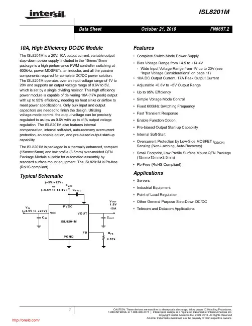
Complete High Efficiency DC/DC Power ModuleISL8204M, ISL8206MThe ISL8204M, ISL8206M is a family of pin-compatible power modules to the ISL8201M. These are simple and easy to use, high power DC/DC modules and are ideal for a wide variety of applications. The ISL820xM family of high current DC/DCstep-down modules virtually eliminate design and manufacturing risks while dramatically improving time to market.The simplicity is in the family's "Off The Shelf" unassisted implementation. All you need is the ISL820xM for the current requirement of your design, bulk input and output capacitors and one resistor, to program the output voltage, and you have a complete high current power design ready for your market.This family of buck converters is packaged in a thermallyenhanced compact (15mmx15mm) over-molded QFN Package that operates without a heat sink, even at full load overtemperature. The package supports simple, reliable, automated assembly using standard surface mount equipment while making it easy to probe to all pins. The lack of a required heat dissipation layer, provides easy access to all pins and the limited number of the external components reduce the PCB to a component layer and a simple ground layer.Additionally, each IC in the family is foot print compatible, making it easy to change your design to meet different power needs without changing your layout. One simple layout fits all.Features•Complete Switch Mode Power Supply in one package -ISL8204M - 4A with, 6.6A Peak -ISL8206M - 6A with, 8.8A Peak•Single Resistor Sets VOUT +0.6V up to +6V @ ±1%•Up to 95% Efficiency •Overcurrent Protection•Internal Soft-Start with Pre-bias Output Start-up •Wide Input Voltage Range from 1VDC to 20VDC •Fast Transient ResponseApplications•Servers•Telecom and Datacom Applications •Industrial Equipment •Point of Load Regulation•General Purpose Step-Down DC/DCRelated Literature•AN1386 “ISL8201M, ISL8204M, ISL8206M EVAL1Z Evaluation Board User’s Guide”•iSim Model - (See Respective Device Information Page at )FIGURE 1.TYPICAL SCHEMATICFIGURE 2.DERATING CURVE (ISL8206M 5V IN )0123456760708090100110AMBIENT TEMPERATURE (°C)M A X L O A D C U R R E N T (A )0.6V1.5V3.3VTABLE 1.R FB VALUES FOR TYPICAL OUTPUT VOLTAGESV OUT 0.6V 1.05V 1.2V 1.5V 1.8V 2.5V 3.3V 5V R FBOpen13k9.76k6.49k4.87k3.09k2.16k1.33kSimplified Block DiagramFIGURE 3.INTERNAL BLOCK DIAGRAM Ordering InformationPART NUMBER (Notes 1, 2, 3)PARTMARKINGTEMP.RANGE (°C)PACKAGE(RoHS Compliant)PKG.DWG.#ISL8204MIRZ ISL8204M-40 to +8515 Ld QFN L15.15x15ISL8206MIRZ ISL8206M-40 to +8515 Ld QFN L15.15x15ISL8204MEVAL1Z Evaluation BoardISL8206MEVAL1Z Evaluation BoardNOTES:1.Add “-T*” suffix for tape and reel. Please refer to TB347 for details on reel specifications.2.These Intersil plastic packaged products employ special material sets, molding compounds and 100% matte tin plate plus anneal (e3) terminationfinish. These products do contain Pb but they are RoHS compliant by EU exemption 5 (Pb in glass of cathode ray tubes, electronic components and fluorescent tubes). These Intersil RoHS compliant products are compatible with both SnPb and Pb-free soldering operations. These Intersil RoHS compliant products are MSL classified at Pb-free peak reflow temperatures that meet or exceed the Pb-free requirements of IPC/JEDEC J STD-020.3.For Moisture Sensitivity Level (MSL), please see device information page for ISL8204M, ISL8206M. For more information on MSL please see techbriefTB363.Summary of FeaturesPART NUMBER RATED CURRENT(A)R ISET(kΩ)LS FET r DS(ON)(mΩ)MAX V OUT(V)ISL8206M6 4.12156 ISL8204M4 2.87156Pin ConfigurationISL8204M, ISL8206M(15 LD QFN)TOP AND 3D VIEWPD2PD3PD4P G N D P G N D P G N DP V C CN C I S E T N CV I NPGND NC PHASE PGNDVOUTCOMP/ENFB 987654321151413121110PD1Pin DescriptionsPIN SYMBOL DESCRIPTION1, 2, 3, 4PGNDPower ground pin for signal, input, and output return path. PGND needs to connect to one (or more) ground plane(s) immediately, which is recommended to minimize the effect of switching noise, copper losses, and maximize heat dissipation. Range: 0V.5 PVCCThis pin provides the bias supply for ISL8204M, ISL8206M, as well as the low-side MOSFET’s gate and high-side MOSFET’s gate. If PVCC rises above 6.5V, an internal 5V regulator will supply to the internal logics bias (but high-side and low-side MOSFET gate will still be sourced by PVCC). Connect a well decoupled +5V or +12V supply to this pin. Connect 1µF ceramic capacitor to ground plane directly. Range: 4.5V to 14.4V. 6, 8, 15 NCNo internal connection.7 ISETThe ISET pin is the input for the overcurrent protection (OCP) setting, which compares the r DS(ON) of the low-side MOSFET to set the overcurrent threshold. The ISL8204M, ISL8206M has an initial protect overcurrent limit. It has an integrated internal 4.12k Ω/2.87k Ω resistor (R SET-IN ) between the ISET and PGND pins, which can prevent significant overcurrent impact to the module. One can also connect an additional resistor R SET-EX between the ISET pin and the PGND pin in order to reduce the current limit point by paralleling. Range: 0 to PVCC.9 VIN(PD1)Power input pin. Apply input voltage between the VIN pin and PGND pin. It is recommended to place an input decoupling capacitor directly between the VIN pin and the PGND pin. The input capacitor should be placed as closely as possible to the module. Range: 1V to 20V.10 PHASE (PD2)The PHASE pin is the switching node between the high and low side MOSFET. It also returns the current path for the high side MOSFET driver and detects the low-side MOSFET drain voltage for the overcurrent limits point. Range: 0V to 30V. 11PGND (PD3)Power ground pin for signal, input, and output return path. PGND needs to connect to one (or more) ground plane(s) immediately, which is recommended to minimize the effect of switching noise, copper losses, and maximize heat dissipation. Range: 0V.12VOUT (PD4)Power output pin. Apply output load between this pin and the PGND pin. It is recommended to place a high frequency output decoupling capacitor directly between the VOUT pin and the PGND pin. The output capacitor should be placed as closely as possible to the module. Range: 0.6V to 6V.Pin Descriptions (Continued)PIN SYMBOL DESCRIPTION13 COMP/EN This is the multiplexed pin of the ISL8204M, ISL8206M. During soft-start and normal converter operation, this pinrepresents the output of the error amplifier. Use COMP/EN in combination with the FB pin to compensate for the voltagecontrol feedback loop of the converter. Pulling COMP/EN low (V ENDIS = 0.4V nominal) will disable (shut-down) thecontroller, which causes the oscillator to stop, and the high-side gate and low-side gate of the MOSFETs outputs to be heldlow. The external pull-down device will initially need to overcome a maximum of 5mA of COMP/EN output current.However, once the controller is disabled, the COMP/EN output will also be disabled, thus only a 20µA current source willcontinue to draw current. Range: 0V to 5V.14 FB The FB pin is the output voltage adjustment of the ISL8204M, ISL8206M. It will regulate to 0.6V at the FB pin withrespect to the PGND pin. The ISL8204M, ISL8206M has an integrated voltage dividing resistor. This is a precision9.76kW resistor (RFB-TI) between the VOUT and FB pins. Different output voltages can be programmed withadditional resistors between FB to PGND. Range: 0.6V.Absolute Maximum Ratings Thermal InformationC OMP/EN to P GND. . . . . . . . . . . . . . . . . . . . . . . . . . . . . . . . P GND - 0.3V to +6V I SET to P GND . . . . . . . . . . . . . . . . . . . . . . . . . . . . . P GND - 0.3V to P VCC + 0.3V P VCC to P GND . . . . . . . . . . . . . . . . . . . . . . . . . . . . . . . . . . P GND - 0.3V to +15V P HASE to P GND (Note 4). . . . . . . . . . . . . . . . . . . . . . . . . . . . . . . . -1.2V ~ +30V V IN to P HASE (Note 4). . . . . . . . . . . . . . . . . . . . . . . . . . . . . . . . . . -1.2V ~ +30V Junction Temperature, T J. . . . . . . . . . . . . . . . . . . . . . . . . . . . . . . . . . +125°C Storage Temperature Range, T STG. . . . . . . . . . . . . . . . . . -40°C to +125°C ESD RatingHuman Body Model (Tested per JESD22-A114E). . . . . . . . . . . . . . . . 2kV Machine Model (Tested per JESD22-A115-A). . . . . . . . . . . . . . . . . 100V Charge Device Model (Tested per JESD22-C101C). . . . . . . . . . . . . . . 1kV Latch Up (Tested per JESD-78B; Class 2, Level A) . . . . . . . . . . . . . . 100mA Thermal Resistance (Typical)θJA(°C/W)θJC(°C/W) 15 Ld QFN (Notes 5, 6) . . . . . . . . . . . . . . . . 13.0 2.0Pb-Free Reflow Profile . . . . . . . . . . . . . . . . . . . . . . . . . . . . . . . see link below /pbfree/Pb-FreeReflow.asp Recommended Operating RatingsInput Supply Voltage (V IN) . . . . . . . . . . . . . . . . . . . . . . . . . . . . . +1V to +20V Output Voltage (V OUT). . . . . . . . . . . . . . . . . . . . . . . . . . . . . . . . . +0.6V to +6V P VCCFixed Supply Voltage . . . . . . . . . . . . . . . . . . . . . . . . . . . . . . . +5V or +12V Wide Range Supply . . . . . . . . . . . . . . . . . . . . . . . . . . . . . +6.5V to +14.4V Ambient Temperature Range (T A) . . . . . . . . . . . . . . . . . . . -40°C to +85°CCAUTION: Do not operate at or near the maximum ratings listed for extended periods of time. Exposure to such conditions may adversely impact product reliability and result in failures not covered by warranty.NOTES:4.V DS (Drain to Source) specification for internal high-side and low-side MOSFET.5.θJA is measured in free air with the component mounted on a high effective thermal conductivity test board (i.e. 4-layer type without thermal vias– see tech brief TB379) per JEDEC standards except that the top and bottom layers assume solid planes.6.ForθJC, the “case temp” location is the center of the exposed metal pad on the package underside.Electrical Specifications TA = +25°C. V IN = 12V, V OUT = 1.5V. C IN = 220µFx1, 10µF/Ceramicx2, C OUT=47µFx8/Ceramic. Boldface limits apply over the operating temperature range, -40°C to +85°C.PARAMETER SYMBOL CONDITIONSMIN(Note 8)TYPMAX(Note 8)UNITSINPUT CHARACTERISTICSInput Supply Bias Current I Q(VIN)I OUT = 0A, V OUT = 1.5V, V IN = 12V, P VCC = 12V - 13 - mA Input Inrush Current I inRush I OUT = 0A, V OUT = 1.5V, V IN = 12V, P VCC = 12V-140-mA Input Supply Current I S(VIN)I OUT = 6A, V OUT = 1.5V, V IN = 12V, P VCC = 12V - 0.86 - AI OUT = 4A, V OUT = 1.5V, V IN = 12V, P VCC = 12V - 0.56 - A OUTPUT CHARACTERISTICSOutput Continuous Current Range I OUT(DC)V IN = 12V, V OUT = 1.5V0 -ISL8206M6AISL8204M0 -4A Line Regulation AccuracyΔV OUT/ΔV IN V OUT = 1.5V, I OUT = 0A, V IN = 3.3V to 20V,P VCC = 5V-0.1-%Load Regulation AccuracyΔV OUT/ΔI OUT I OUT = 0A to 6A/4A, V OUT = 1.5V, V IN=12V,P VCC= 12V- 0.5 - % Peak-to-Peak Output Ripple VoltageΔV OUT ISL8206M - 8 - mVI OUT = 6A V OUT = 1.5V, V IN = 12V,P VCC = 12VISL8204M - 7 - mVI OUT = 4A V OUT = 1.5V, V IN = 12V,P VCC = 12VDYNAMIC CHARACTERISTICSVoltage Change For Positive Load StepΔV OUT-DP I OUT = 0A to 4A. Current slew rate=2.5A/µs,V IN = 12V, V OUT = 1.5V, P VCC=12V- 30 - mVVoltage Change For Negative Load StepΔV OUT-DN I OUT = 0A to 4A. Current slew rate=2.5A/µs,V IN = 12V, V OUT = 1.5V, P VCC=12V- 27 - mVVoltage Change For Positive Load Step ΔV OUT-DP I OUT = 0A to 6A. Current slew rate =2.5A/µs, V IN = 12V, V OUT = 1.5V, P VCC =12V- 43 - mV Voltage Change For Negative Load Step ΔV OUT-DNI OUT = 0A to 6A. Current slew rate =2.5A/µs, V IN = 12V, V OUT = 1.5V, P VCC =12V-40-mVCONTROLLERPVCC Supply Current Shutdown I PVCC_S P VCC = 12V; Disabled (Note 7) 4 5.27 mA Supply VoltageP VCCFixed 5V supply (Note 7) 4.5 5.0 5.5 V Wide range supply (Note 7)6.512.0 14.4VP VCC Operating CurrentI PVCCI OUT = 6A, V OUT = 1.5V, V IN =12V 5V supply -14 - mA 12V supply-25-mAI OUT = 4A, V OUT = 1.5V, V IN =12V 5V supply -14 - mA 12V supply-25-mA Rising P VCC ThresholdV PORR (Note 7) 3.9 4.1 4.3V P VCC Power-On-Reset Threshold Hysteresis V PORH (Note 7) 0.30 0.35 0.40V Oscillator FrequencyF OSC (Note 7) 510 600 660kHz Internal Resistor Between V OUT and FB Pins R FB-TI(Note 7)9.66 9.76 9.86k ΩDisabled Threshold Voltage (COMP/EN)V ENDIS (Note 7)0.375 0.4 0.425V Reference VoltageV REF(Note 7)- 0.6- V Reference Voltage Tolerance0°C to +70°C (Note 7)-1.0- +1.0%-40°C to +85°C (Note 7)-1.5- +1.5%FAULT PROTECTIONInternal Resistor Between I SET and P GND PinsR SET-INISL8206M - 4.12- k ΩISL8204M- 2.87- k ΩI SET Current Source I SET (Note 7)18.021.523.5µANOTES:7.Parameters are 100% tested for internal IC/component prior to module assembly.8.Parameters with MIN and/or MAX limits are 100% tested at +25°C, unless otherwise specified. Temperature limits established by characterizationand are not production tested.Electrical SpecificationsT A = +25°C. V IN = 12V, V OUT = 1.5V. C IN = 220µFx1, 10µF/Ceramicx2, C OUT =47µFx8/Ceramic. Boldface limitsapply over the operating temperature range, -40°C to +85°C. (Continued)PARAMETERSYMBOL CONDITIONSMIN (Note 8)TYP MAX (Note 8)UNITSFIGURE 4.TEST CIRCUIT FOR ALL PERFORMANCE AND DERATING GRAPHSTypical Performance CharacteristicsEfficiency PerformanceT A = +25°C, V IN = P VCC (P VCC = 5V for 18V IN ), C IN = 220µFx1, 10µF/Ceramic x 2, C OUT = 330µF (ESR = 10m Ω), 22µF/Ceramic x 3. The efficiency equation is:FIGURE 5.EFFICIENCY vs LOAD CURRENT (5V IN )FIGURE 6.EFFICIENCY vs LOAD CURRENT (12V IN )FIGURE 7.EFFICIENCY vs LOAD CURRENT (18V IN )Efficiency Output PowerInput Power-----------------------------------------P OUT P IN ---------------V OUT xI OUT ()V IN xI IN ()--------------------------------------===60657075808590951000246LOAD CURRENT (A)E F F I C I E N C Y (%)1353.3V2.5V1.5V1.2V0.8V6065707580859095100LOAD CURRENT (A)E F F I C I E N C Y (%)2461353.3V2.5V1.5V1.2V0.8V5.0V60657075808590951000LOAD CURRENT (A)E F F I C I E N C Y (%)5.0V3.3V2.5V1.5V1.2V123456Typical Performance Characteristics (Continued)Transient Response PerformanceT A = +25°C, V IN = 12V, P VCC = 12V, C IN =220µFx1, 10µF/Ceramic x 2, C OUT =330µF (ESR = 10m Ω), 22µF/Ceramic x 3 IOUT = 0A to 5A, Current slew rate = 2.5A/µsFIGURE 8.1.2V TRANSIENT RESPONSE FIGURE 9.1.5V TRANSIENT RESPONSEFIGURE 10.1.8V TRANSIENT RESPONSE FIGURE 11.2.5V TRANSIENT RESPONSEFIGURE 12.3.3V TRANSIENT RESPONSEV IN = 12V V OUT = 1.2V I OUT = 0A to 5AI OUT V OUTV IN = 12V V OUT = 1.5V I OUT = 0A to 5AV OUTI OUTV IN = 12V V OUT = 1.8V I OUT = 0A to 5AV OUTI OUTV IN = 12V V OUT = 2.5V I OUT = 0A to 5AV OUTI OUTV IN = 12V V OUT = 3.3V I OUT = 0A to 5AV OUTI OUTTypical Performance Characteristics (Continued)Output Ripple PerformanceT A = +25°C, V OUT = 1.5V, C IN = 220µFx1, 10µF/Ceramic x 2, C OUT = 47µF/Ceramic x 8. Oscilloscope BW = 20MHzFIGURE 13.OUTPUT VOLTAGE RIPPLE AT V IN = 5V FIGURE 14.OUTPUT VOLTAGE RIPPLE AT V IN = 12VV OUT 6AV OUT 4A V OUT 0AV OUT 6AV OUT 4AV OUT 0AReference Circuitry For General Applications1.Single Power SupplyFigure 15 shows the ISL8204M, ISL8206M application schematic for input voltage +5V or +12V. The PVCC pin can2.Separated Power SupplyFigure 16 shows the ISL8204M, ISL8206M application schematic for wide input voltages from +1V to +20V. The P VCC supply can source +5V/+12V or +6.5V to 14.4V.Applications InformationThe typical ISL8204M, ISL8206M application schematic for inputvoltage +5V or +12V is shown in Figure 15. External component selection is primarily determined by the maximum load current and input/output voltage.Programming the Output VoltageThe ISL8204M, ISL8206M has an internal 0.6V ±1.5% reference voltage. Programming the output voltage requires a dividing resistor (R FB ). The output voltage can be calculated as shown in Equation 1:Note: ISL8204M, ISL8206M has integrated 9.76k Ω resistance into the module (dividing resistor for top side). The resistancecorresponding to different output voltages is as shown in Table 2:Initialization (POR and OCP Sampling)Figure 17 shows a start-up waveform of ISL8204M, ISL8206M. The power-on-reset (POR) function continually monitors the bias voltage at the PVCC pin. Once the rising POR threshold has exceeded 4V (V PORR nominal), the POR function initiates the overcurrent protection (OCP) sample and hold operation (while COMP/EN is ~1V). When the sampling is complete, V OUT beginsthe soft-start ramp.If the COMP/EN pin is held low during power-up, the initialization will be delayed until the COMP/EN is released and its voltage rises above the V ENDIS trip point.Figure 18 and Figure 19 show a typical power-up sequence in more detail. The initialization starts at T 0, when either P VCC rises above V PORR , or the COMP/EN pin is released (after POR). The COMP/EN will be pulled up by an internal 20µA current source, however, the timing will not begin until the COMP/EN exceeds the V ENDIS trip point (at T 1). The external capacitance of the disabling device, as well as the compensation capacitors, will determine how quickly the 20µA current source will charge the COMP/EN pin. With typical values, it should add a small delay compared to the soft-start times. The COMP/EN will continue to ramp to ~1V.FIGURE 15.TYPICAL APPLICATION SCHEMATICFIGURE 16.WIDE INPUT VOLTAGE APPLICATION SCHEMATICV OUT 0.619.76kRFB--------------+⎝⎠⎛⎞×=(EQ. 1)TABLE 2.RESISTANCE TO OUTPUT VOLTAGES V OUT 0.6V 0.8V 1.05V 1.2V R FB open 28.7k Ω13k Ω9.76k ΩV OUT 1.5V 1.8V 2.5V 3.3V R FB6.49k Ω 4.87k Ω 3.09k Ω2.16k ΩV OUT 5V 6V R FB1.33k Ω1.07k ΩFIGURE 17.POR AND SOFT-START OPERATIONV OUTCOMP/EN~4VPVCC分销商库存信息:INTERSILISL8204MIRZ ISL8206MIRZ ISL8204MIRZ-T ISL8206MIRZ-T。