LI-ion(新)电池充电常识_图文
- 格式:pdf
- 大小:135.43 KB
- 文档页数:19
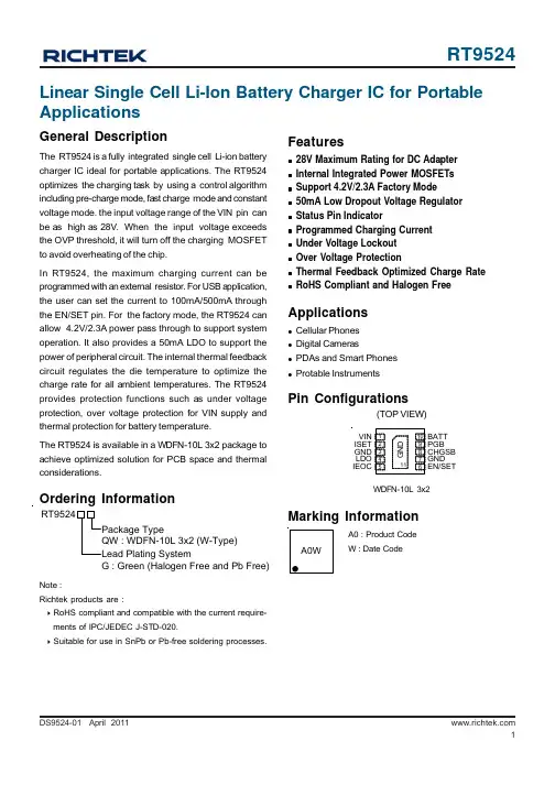
DS9524-01 April 2011Ordering InformationNote :Richtek products are :` RoHS compliant and compatible with the current require-ments of IPC/JEDEC J-STD-020.` Suitable for use in SnPb or Pb-free soldering processes.Pin ConfigurationsWDFN-10L 3x2(TOP VIEW)Linear Single Cell Li-Ion Battery Charger IC for Portable ApplicationsGeneral DescriptionThe RT9524 is a fully integrated single cell Li-ion battery charger IC ideal for portable applications. The RT9524optimizes the charging task by using a control algorithm including pre-charge mode, fast charge mode and constant voltage mode. the input voltage range of the VIN pin can be as high as 28V. When the input voltage exceeds the OVP threshold, it will turn off the charging MOSFET to avoid overheating of the chip.In RT9524, the maximum charging current can be programmed with an external resistor. For USB application,the user can set the current to 100mA/500mA through the EN/SET pin. For the factory mode, the RT9524 can allow 4.2V/2.3A power pass through to support system operation. It also provides a 50mA LDO to support the power of peripheral circuit. The internal thermal feedback circuit regulates the die temperature to optimize the charge rate for all ambient temperatures. The RT9524provides protection functions such as under voltage protection, over voltage protection for VIN supply and thermal protection for battery temperature.The RT9524 is available in a WDFN-10L 3x2 package to achieve optimized solution for PCB space and thermal considerations.Featuresz 28V Maximum Rating for DC Adapter z Internal Integrated Power MOSFETs z Support 4.2V/2.3A Factory Modez 50mA Low Dropout Voltage Regulator z Status Pin Indicatorz Programmed Charging Current z Under Voltage Lockout z Over Voltage Protectionz Thermal Feedback Optimized Charge Rate zRoHS Compliant and Halogen FreeApplicationsz Cellular Phones z Digital Camerasz PDAs and Smart Phones zProtable InstrumentsMarking InformationA0 : Product CodeW : Date CodeISET IEOCGND PGB CHGSB GND EN/SETLDOVIN BATT G : Green (Halogen Free and Pb Free)Typical Application CircuitFunction Block DiagramDS9524-01 April 2011Electrical CharacteristicsTo be continuedRecommended Operating Conditions (Note 3)z Supply Input Voltage, V IN ----------------------------------------------------------------------------------------------4.3V to 5.5V z Junction T emperature Range ------------------------------------------------------------------------------------------−40°C to 125°C zAmbient T emperature Range ------------------------------------------------------------------------------------------ −20°C to 85°CAbsolute Maximum Ratings (Note 1)z Supply Input Voltage, V IN ----------------------------------------------------------------------------------------------−0.3V to 28V z Other Pins -----------------------------------------------------------------------------------------------------------------−0.3V to 6V zPower Dissipation, P D @ T A = 25°CWDFN-10L 3x2----------------------------------------------------------------------------------------------------------- 1.111W zPackage Thermal Resistance (Note 2)WDFN-10L 3x2, θJA ------------------------------------------------------------------------------------------------------90°C/W WDFN-10L 3x2, θJC -----------------------------------------------------------------------------------------------------15°C/W z Lead Temperature (Soldering, 10 sec.)-----------------------------------------------------------------------------260°C z Junction T emperature ---------------------------------------------------------------------------------------------------150°CzStorage Temperature Range -------------------------------------------------------------------------------------------−65°C to 150°C(V IN= 5V, V BATT = 4V, T A = 25°C, unless otherwise specified)Note 1. Stresses listed as the above“Absolute Maximum Ratings”may cause permanent damage to the device. These are for stress ratings. Functional operation of the device at these or any other conditions beyond those indicated in the operational sections of the specifications is not implied. Exposure to absolute maximum rating conditions for extended periods may remain possibility to affect device reliability.Note 2. θJA is measured in the natural convection at T A = 25°C on a high effective thermal conductivity four-layer test board of JEDEC 51-7 thermal measurement standard. The measurement case position of θJC is on the exposed pad of the package.Note 3. The device is not guaranteed to function outside its operating conditions.DS9524-01 April 2011VOUT Regulation Voltage vs. Input Voltage4.1954.2004.2054.2104.2154.2204.2254.54.945.385.826.266.7Input Voltage (V)V O U T R e g u l a t i o n V o l t a g e (V)VOUT Sleep Leakage Current vs. Battery Voltage0481216201.31.72.12.52.93.33.74.14.5Battery Voltage (V)V O U T S l e e p L e a k a g e C u r r e n t (µA )Input OVP Threshold vs. Temperature6.706.726.746.766.786.806.826.84-50-25255075100125Temperature (°C)I n p u t O V P T h r e s h o l d (V )Typical Operating CharacteristicsLDO Voltage vs. Temperature4.854.874.894.914.934.95-50-25255075100125Temperature (°C)L D O V o l t a g e (V)LDO Output Voltage vs. Output Current4.854.874.894.914.934.9520406080100Output Current (mA)L D O O u t p u t V o l t a g e (V)VOUT Regulation Voltage vs. Temperature4.1854.1904.1954.2004.2054.2104.215-50-25255075100125Temperature (°C)V O U T R e g u l a t i o n V o l t a g e (V )EN/SET Shut-DownTime (1ms/Div)V IN = 5VEN/SEB (1V/Div)VLDO (2V/Div)I CHARGER (500mA/Div)CHGS (2V/Div)Power On Time (10ms/Div)PGB (2V/Div)V IN (5V/Div)V BATT = 3.8V, R ISET = 680Ω, EN/SEB = LowCHGSB (2V/Div)I CHARGER (500mA/Div)USB 100 Mode Charge Current vs. Input Voltage8590951004.54.95.35.76.16.5Input Voltage (V)Ch a r g e C u r r e n t (m A )ISET Voltage vs. Input Voltage1.471.481.491.501.511.521.534.24.725.245.766.286.8Input Voltage (V)I S E T V o l t a g e (V )USB 500 Mode Charge Current vs. Input Voltage3653753853954054154.54.95.35.76.16.5Input Voltage (V)Ch a r g e C u r r e n t (m A )ISET Mode Charge Current vs. Input Voltage3003754505256006757508259004.54.95.35.76.16.5Input Voltage(V)C h a r ge C u r r e n t (m A )DS9524-01 April 2011Factory ModeTime (50μs/Div)V IN = 5V , C OUT = 44μF, I OUT = 10Ω to 2.3ΩVIN (5V/Div)VBA TT (200mV/Div)EN/SET (1V/Div)I OUT (1A/Div)LDO Load Transient ResponseTime (250μs/Div)V IN = 5V, V BATT = 3.8V, I LDO = 5mA to 50mAVLDO _ac(100mV/Div)I LDO(500mA/Div)Time (1ms/Div)V IN = 5V, V BATT = 3.8V, R ISET = 680ΩVIN (5V/Div)VBA TT (5V/Div)EN/SET (2V/Div)I CHARGER (500mA/Div)VIN (5V/Div)VBA TT(5V/Div)EN/SET (2V/Div)I CHARGER (500mA/Div)V IN = 5V, V BATT = 3.8V, R ISET = 80ΩTime (1ms/Div)Application InformationDescriptionThe RT9524 is a fully integrated low cost single-cell Li-Ion battery charger IC with a constant current mode (CC mode) or a constant voltage mode (CV mode). The charge current is programmable to USB100, USB500 or ISET mode and the CV mode voltage is fixed at 4.2V. The pre-charge threshold is fixed at 2.5V. If the battery voltage is below the pre-charge threshold, the RT9524 charges the battery with a trickle current until the battery voltage rises above the pre-charge threshold. The RT9524 is capable of being powered up from AC adapter and USB (Universal Serial Bus) port inputs. Moreover, the RT9524 include a linear regulator (LDO 4.9V, 50mA) for supplying low power external circuitry.ACIN Over Voltage ProtectionThe input voltage is monitored by the internal comparator and the input over voltage protection threshold is set to 6.9V. However, input voltage over 28V will still cause damage to the RT9524. When the input voltage exceeds the threshold, the comparator outputs a logic signal to turn off the power P-MOSFET to prevent the high input voltage from damaging the electronics in the handheld system. When the input over voltage condition is removed, the comparator re-enables the output by running through the soft-start.Charger Enable and mode SettingEN/SET is used to enable or disable the charger as well as to select the charge current limit. Drive the EN pin to low or leave it floating to enable the charger. The EN/SET pin has a 200kΩ internal pull down resistor. So, when left floating, the input is equivalent to logic low. Drive this pin to high to disable the charger. After the EN/SET pin pulls low for 50μs, the RT9524 enters the USB500 mode and wait for the setting current signal. EN/SET can be used to program the charge current during this cycle. The RT9524 will change its charge current by sending different pulse to EN/SET pin. If no signal is sent to EN/SET, the RT9524 will remain in USB500 mode. A correct period of time for high pulse is between 100μs and 700μs and the period of pulse to pulse must be between 100μs and 700μs to be properly read. Once EN/SET is held low for 1.5ms,the number of pulses is locked and sent to the control logic and then the mode changes. The RT9524 needs to be restarted to reset the charge current. Once the EN/ SET input is held high for more than 1.5ms, the RT9524 is disabled.Table 1. Pulse Counting Map for EN/SET InterfaceFigure .1 (b)Battery Charge ProfileThe RT9524 charges a Li-Ion battery with a constant current (CC) or a constant voltage (CV).The constant current is decided by the operation mode of USB100, USB500 or ISET mode. The constant current is set with the external resistor R ISET and the constant voltage is fixed at 4.2V. If the battery voltage is below the Pre-Charge Threshold, the RT9524 charges the battery with a trickle current until the battery voltage rises above the trickle charge threshold. When the battery voltage reaches 4.2V, the charger enters CV mode and regulates the battery voltage at 4.2V to fully charge the battery without the risk of over chargingFigure .1 (a)IIDS9524-01 April 2011Battery Pre-Charge CurrentDuring a charge cycle, if the battery voltage is below the pre-charge threshold, the RT9524 enters the pre-charge mode. This feature revives deeply discharged cells and protects battery. Under USB100 Mode, the pre-charge current is internally set to 95mA. When the RT9524 is under USB500 and ISET Mode, the pre-charge current is 20% of fast-charge current set by external resistor R ISET .Battery Fast-Charge Current ISET ModeThe RT9524 offers ISET pin to program the charge current.The resistor R ISET is connected to ISET and GND. The parameter K ISET is specified in the specification table.ISEF Charge ISEF ISETKI = ; K = 530R USB500 and USB100 ModeThe fast-charge current is 95mA in USB100 mode and 395mA in USB500 mode. Note that if the fast-charge current set by external resistor is smaller than that in USB500 mode (395mA), the RT9524 charges the battery in ISET mode.Battery Voltage Regulation (CV Mode)The battery voltage regulation feedback is through the BATT pin. The RT9524 monitors the battery voltage between BATT and GND pins. When the battery voltage closes in on the battery regulation voltage threshold, the voltage regulation phase begins and the charging current begins to taper down. When the charging current falls below the programmed end-of-charge current threshold,the CHGSB pin goes high to indicate the termination of charge cycle.The end-of-charge current threshold is set by the IEOC pin. The resistor R EOC is connected to IEOC and GND.The parameters K EOC and IEOC are specified in the specification table.EOC EOC EOC EOC RI (%) = ; K = 200K The current threshold of IEOC (%) is defined as the percentage of fast-charge current set by R ISET . After the CHGSB pin is pulled high, the RT9524 still monitors the battery voltage. Charge current is resumed when the battery voltage goes to lower than the battery regulation voltage threshold.Factory ModeThe RT9524 provides factory mode for supplies up to 2.3A for powering external loads with no battery installed and BATT is regulated to 4.2V. The factory mode allows the user to supply system power with no battery connected.In factory mode, thermal regulation is disabled but thermal protection (155°C) is still active. When using currents greater than 1.5A in factory mode, the user must limit the duty cycle at the maximum current to 20% with a maximum period of 10ms.LDOThe RT9524 integrates one low dropout linear regulator(LDO) that supplies up to 50mA. The LDO is active whenever the input voltage is between POR threshold andFigure 2Figure 32004006008001000120014000.40.60.81 1.2 1.4 1.61.82 2.22.4 2.62.83R SET ∠)B a t t e r yC h a r g e C u r r e n t (m A )(k ΩOVP threshold. It is not affected by the EN/SET input.Note that the LDO current is independence and not monitored by the charge current limit.Charge Status Outputs (CHGSB and PGB)The open-drain CHGSB and PGB outputs indicate various charger operations as shown in the following table. These status pins can be used to drive LEDs or communicate to the host processor. Note that ON indicates the open-drain transistor is turned on and LED is bright.Table 2Sleep ModeThe RT9524 enters sleep mode if the power is removed from the input. This feature prevents draining the battery during the absence of input supply.Temperature Regulation and Thermal Protection In order to maximize charge rate, the RT9524 features a junction temperature regulation loop. If the power dissipation of the IC results in a junction temperature greater than the thermal regulation threshold (125°C), the RT9524 limits the charge current in order to maintain a junction temperature around the thermal regulation threshold (125°C). The RT9524 monitors the junctiontemperature, T J , of the die and disconnects the battery from the input if T J exceeds 125°C. This operation continues until junction temperature falls below thermal regulation threshold (125°C) by the hysteresis level. This feature prevents maximum power dissipation from exceeding typical design conditions.Selecting the Input and Output CapacitorsIn most applications, all that is needed is a high-frequency decoupling capacitor on the input. A 1μF ceramic capacitor,placed in close proximity to input to GND, works well. Insome applications depending on the power supplycharacteristics and cable length, it may be necessary toadd an additional 10μF ceramic capacitor to the input.The RT9524 requires a small output capacitor for loop stability. A typical 1μF ceramic capacitor placed between the BATT pin and GND is sufficient.Thermal ConsiderationsFor continuous operation, do not exceed absolutemaximum operation junction temperature. The maximum power dissipation depends on thermal resistance of the IC package, PCB layout, rate of surrounding airflow, and difference between junction and ambient temperature. Themaximum power dissipation can be calculated by thefollowing formula :P D(MAX) = (T J(MAX) − T A ) / θJAwhere T J(MAX) is the maximum operation junctiontemperature, T A is the ambient temperature, and θJA is thejunction to ambient thermal resistance.For recommended operating conditions specification of RT9524, the maximum junction temperature is 125°C and T A is the maximum ambient temperature. The junction to ambient thermal resistance, θJA , is layout dependent. For WDFN-10L 3x2 packages, the thermal resistance, θJA , is 90°C/W on a standard JEDEC 51-7 four-layer thermal test board. The maximum power dissipation at T A = 25°C can be calculated by the following formula :P D(MAX) = (125°C − 25°C) / (90°C/W) = 1.111W for WDFN-10L 3x2 packageThe maximum power dissipation depends on operating ambient temperature for fixed T J(MAX) and thermal resistance, θJA . For RT9524 package, the derating curveRT952411DS9524-01 April 2011in Figure 4 allows the designer to see the effect of rising ambient temperature on the maximum power dissipation.Figure 4. Derating Curve for RT9524 Package Layout ConsiderationThe RT9524 is a fully integrated low cost single-cell Li-Ion battery charger IC ideal for portable applications. Careful PCB layout is necessary. For best performance, place all peripheral components as close to the IC as possible. A short connection is highly recommended. The following guidelines should be strictly followed when designing a PCB layout for the RT9524.`Input capacitor should be placed close to the IC and connected to ground plane. The trace of input in the PCB should be placed far away from the sensitive devices or shielded by the ground.`The GND should be connected to a strong ground plane for heat sinking and noise protection.`The connection of R ISET and R IEOC should be isolated from other noisy traces. The short wire is recommended to prevent EMI and noise coupling.`Output capacitor should be placed close to the IC and connected to ground plane to reduce noise coupling.Figure 5. PCB Layout GuideThe capacitor should be placed close to IC pin and The connection of resistor should be isolated from other noisy traces. Short to prevent EMI and noise coupling.ground plane for heat sinking and noise protection.0.00.20.40.60.81.01.2255075100125Ambient Temperature (°C)M a x i m u m P o w e r D i s s i p a t i o n (W )12DS9524-01 April 2011Richtek Technology CorporationHeadquarter5F, No. 20, Taiyuen Street, Chupei City Hsinchu, Taiwan, R.O.C.Tel: (8863)5526789 Fax: (8863)5526611Richtek Technology CorporationTaipei Office (Marketing)5F, No. 95, Minchiuan Road, Hsintien City Taipei County, Taiwan, R.O.C.Tel: (8862)86672399 Fax: (8862)86672377Email:*********************Information that is provided by Richtek Technology Corporation is believed to be accurate and reliable. Richtek reserves the right to make any change in circuit design, specification or other related things if necessary without notice at any time. No third party intellectual property infringement of the applications should be guaranteed by users when integrating Richtek products into any application. No legal responsibility for any said applications is assumed by Richtek.W-Type 10L DFN 3x2 Package。
锂离子电池原理及工艺流程一、原理正极构造LiCoO2(钴酸锂)+导电剂(乙炔黑)+粘合剂(PVDF)+集流体(铝箔)负极构造石墨+导电剂(乙炔黑)+增稠剂(CMC)+粘结剂(SBR)+ 集流体(铜箔)3.0工作原理3.1 充电过程如上图一个电源给电池充电,此时正极上的电子e从通过外部电路跑到负极上,正锂离子Li+从正极“跳进”电解液里,“爬过”隔膜上弯弯曲曲的小洞,“游泳”到达负极,与早就跑过来的电子结合在一起。
正极上发生的反应为LiCoO2=充电=Li1-xCoO2+Xli++Xe(电子)负极上发生的反应为6C+XLi++Xe=====LixC63.2 电池放电过程放电有恒流放电和恒阻放电,恒流放电其实是在外电路加一个可以随电压变化而变化的可变电阻,恒阻放电的实质都是在电池正负极加一个电阻让电子通过。
由此可知,只要负极上的电子不能从负极跑到正极,电池就不会放电。
电子和Li+都是同时行动的,方向相同但路不同,放电时,电子从负极经过电子导体跑到正极,锂离子Li+从负极“跳进”电解液里,“爬过”隔膜上弯弯曲曲的小洞,“游泳”到达正极,与早就跑过来的电子结合在一起。
二、工艺流程三、电池不良项目及成因:1.容量低产生原因:a. 附料量偏少;b. 极片两面附料量相差较大;c. 极片断裂;d. 电解液少;e. 电解液电导率低;f. 正极与负极配片未配好;g. 隔膜孔隙率小;h. 胶粘剂老化→附料脱落;i.卷芯超厚(未烘干或电解液未渗透)j. 分容时未充满电;k. 正负极材料比容量小。
2.内阻高产生原因:a. 负极片与极耳虚焊;b. 正极片与极耳虚焊;c. 正极耳与盖帽虚焊;d. 负极耳与壳虚焊;e. 铆钉与压板接触内阻大;f. 正极未加导电剂;g. 电解液没有锂盐;h. 电池曾经发生短路;i. 隔膜纸孔隙率小。
3.电压低产生原因:a. 副反应(电解液分解;正极有杂质;有水);b. 未化成好(SEI膜未形成安全);c. 客户的线路板漏电(指客户加工后送回的电芯);d. 客户未按要求点焊(客户加工后的电芯);e. 毛刺;f. 微短路;g. 负极产生枝晶。
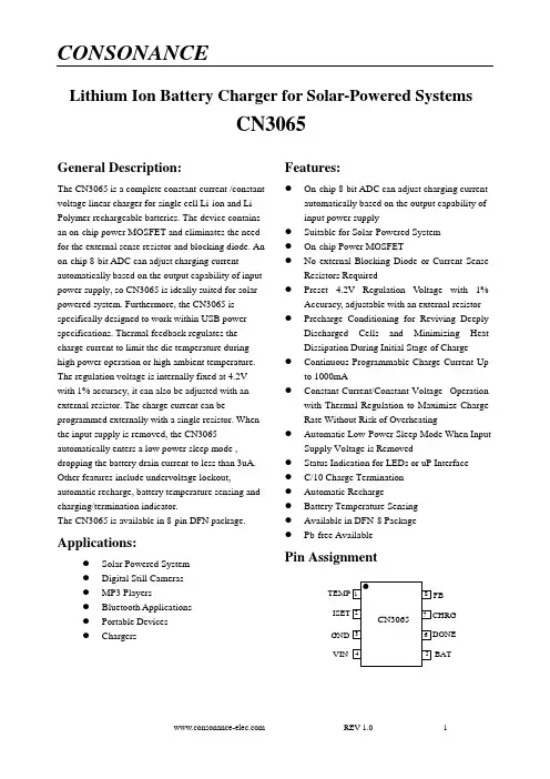
Lithium Ion Battery Charger for Solar-Powered SystemsCN3065General Description:The CN3065 is a complete constant-current /constant voltage linear charger for single cell Li-ion and Li Polymer rechargeable batteries. The device contains an on-chip power MOSFET and eliminates the need for the external sense resistor and blocking diode. An on-chip 8-bit ADC can adjust charging current automatically based on the output capability of input power supply, so CN3065 is ideally suited for solar powered system. Furthermore, the CN3065 is specifically designed to work within USB power specifications. Thermal feedback regulates the charge current to limit the die temperature during high power operation or high ambient temperature. The regulation voltage is internally fixed at 4.2V with 1% accuracy, it can also be adjusted with an external resistor. The charge current can be programmed externally with a single resistor. When the input supply is removed, the CN3065 automatically enters a low power sleep mode , dropping the battery drain current to less than 3uA. Other features include undervoltage lockout, automatic recharge, battery temperature sensing and charging/termination indicator.The CN3065 is available in 8-pin DFN package. Applications:●Solar Powered System●Digital Still Cameras●MP3 Players●Bluetooth Applications●Portable Devices●Chargers Features:●On-chip 8-bit ADC can adjust charging currentautomatically based on the output capability ofinput power supply●Suitable for Solar-Powered System●On-chip Power MOSFET●No external Blocking Diode or Current SenseResistors Required●Preset 4.2V Regulation V oltage with 1%Accuracy, adjustable with an external resistor●Precharge Conditioning for Reviving DeeplyDischarged Cells and Minimizing Heat Dissipation During Initial Stage of Charge●Continuous Programmable Charge Current Upto 1000mA●Constant-Current/Constant-Voltage Operationwith Thermal Regulation to Maximize ChargeRate Without Risk of Overheating●Automatic Low-Power Sleep Mode When InputSupply Voltage is Removed●Status Indication for LEDs or uP Interface●C/10 Charge Termination●Automatic Recharge●Battery Temperature Sensing●Available in DFN-8 Package●Pb-free AvailablePin AssignmentTEMP FBGNDVIN BATCHRGDONETypical Application CircuitInput Power Supply 4.4V to 6VFigure 1 Typical Application Circuit(Constant V oltage Level 4.2V) Input Power Supply 4.4V to 6VFigure 2 Application Circuit(Adjust Constant V oltage Level with Rx)In Figure 2, the BAT pin’s voltage in constant voltage mode is given by the following equation:Vbat = 4.2+3.04×10⁻⁶×RxWhere,Vbat is in voltRx is in ohmBlock DiagramFigure 3 Block DiagramPin DescriptionPin No. Name Function Description1 TEMPTemperature Sense Input. Connecting TEMP pin to NTC thermistor’soutput in Lithium ion battery pack. If TEMP pin’s voltage is below 46% ofinput supply voltage V IN for more than 0.15S, this means that battery’stemperature is too high or too low, charging is suspended. If TEMP’s voltagelevel is above 46% of input supply voltage for more than 0.15S, battery faultstate is released, and charging will resume.The temperature sense function can be disabled by grounding the TEMP pin.2 ISETConstant Charge Current Setting and Charge Current Monitor Pin. Thecharge current is set by connecting a resistor R ISET from this pin to GND.When in precharge mode, the ISET pin’s voltage is regulated to 0.2V. When inconstant charge current mode, the ISET pin’s voltage is regulated to 2V. In allmodes during charging, the voltage on ISET pin can be used to measure thecharge current as follows:I CH = (V ISET/R ISET)×9003 GNDGround Terminal.4 VINPositive Input Supply Voltage. V IN is the power supply to the internal circuit.When V IN drops to within 40mv of the BAT pin voltage, CN3065 enters lowpower sleep mode, dropping BAT pin’s current to less than 3uA.5 BATBattery Connection Pin. Connect the positive terminal of the battery to BATpin. BAT pin draws less than 3uA current in chip disable mode or in sleepmode. BAT pin provides charge current to the battery and provides regulationvoltage of 4.2V.6Open-Drain Charge termination Status Output. In charge terminationstatus, is pulled low by an internal switch; Otherwise pin is inhigh impedance state.7Open Drain Charge Status Output. When the battery is being charged, thepin is pulled low by an internal switch, otherwise pin is in highimpedance state.8 FBBattery Voltage Kevin Sense Input. This Pin can Kelvin sense the batteryvoltage; Also the regulation voltage in constant voltage mode can be adjustedby connecting an external resistor between FB pin and BAT pin. Absolute Maximum RatingsAll Terminal V oltage……………-0.3V to 6.5V Maximum Junction Temperature…...150℃BAT Short-Circuit Duration………...Continuous Operating Temperature…...-40℃ to 85℃Storage Temperature….............-65℃ to 150℃ Thermal Resistance (DFN-8)………….TBDLead Temperature(Soldering)…….............300℃Stresses beyond those listed under ‘Absolute Maximum Ratings’ may cause permanent damage to the device. These are stress ratings only and functional operation of the device at these or any other conditions above those indicated in the operational sections of the specifications is not implied. Exposure to Absolute Maximum Rating Conditions for extended periods may affect device reliability.Electrical Characteristics(VIN=5V, T A=-40℃ to 85℃, Typical Values are measured at T A=25℃,unless otherwise noted) Parameters Symbol TestConditions Min Typ Max Unit Input Supply Voltage VIN 4.4 6 V Operating Current I VIN Charge Termination Mode 400 650 950uA Undervoltage Lockout Vuvlo VIN falling 3.7 3.9V Undervoltage LockoutHysteresisHuvlo 0.1 V Regulation Voltage V REG Constant Voltage Mode 4.158 4.2 4.242 VR ISET=2K, V BAT=3.6V 720 900 1080R ISET=2K, V BAT=2.4V45 90 135mAV BAT=V REG, standby mode 1.75 3.5 7 BAT pin Current I BATVIN=0V, sleep mode 3uA Precharge ThresholdPrecharge Threshold V PRE Voltage at BAT pin rising 2.9 3.0 3.1 VPrecharge Threshold Hysteresis H PRE 0.1VCharge Termination ThresholdCharge TerminationThresholdVterm Measure voltage at ISET pin 0.18 0.22 0.26 V Recharge ThresholdRecharge Threshold V RECH V REG-0.1 V Sleep ModeSleep Mode Threshold V SLP V IN from high to low, measuresthe voltage (V IN-V BAT)40 mvSleep mode Release Threshold V SLPRV IN from low to high, measuresthe voltage (V IN-V BAT)90 mvISET PinPrecharge mode 0.2ISET Pin Voltage V ISETConstant current mode 2.0VTEMP PINInput Threshold V TEMP43.5 46 48.5%V INTEMP input Current TEMP to V IN or to GND 0.5uAPinSink Current I DONE V DONE=0.3V, termination mode 10 mA Leakage Current V DONE=6V, charge mode 1 uAPinSink Current I CHRG V CHRG=0.3V, Charge status 10 mALeakage Current V CHRG=6V, termination mode 1 uADetailed DescriptionThe CN3065 is a linear battery charger designed primarily for charging single cell lithium-ion orlithium-polymer batteries. Featuring an internal P-channel power MOSFET, the charger uses aconstant-current/constant-voltage to charge the batteries. Continuous charge current can be programmed up to 1000mA with an external resistor. No blocking diode or sense resistor is required. The on-chip 8-bit ADC can adjust charging current automatically based on the output capability of input power supply, so CN3065 is ideally suited for the solar-powered systems, or the applications that need to charge lithium-ion battery or lithiumpolymer battery with an input power supply whose output capability is limited. The open-drain outputand indicates the charger’s status. The internal thermal regulation circuit reduces the programmed charge current if the die temperature attempts to rise above a preset value of approximately 115℃. This feature protects the CN3065 from excessive temperature, and allows the user to push the limits of the power handling capability of a given circuit board without risk of damaging the CN3065 or the external components. Another benefit of adopting thermal regulation is that charge current can be set according to typical, not worst-case, ambient temperatures for a given application with the assurance that the charger will automatically reduce the current in worst-case conditions.The charge cycle begins when the voltage at the V IN pin rises above the UVLO level, a current set resistor isconnected from the ISET pin to ground. The pin outputs a logic low to indicate that the charge cycle is ongoing. At the beginning of the charge cycle, if the voltage at FB pin is below 3V, the charger is in precharge mode to bring the cell voltage up to a safe level for charging. The charger goes into the fast chargeconstant-current mode once the voltage on the FB pin rises above 3V. In constant current mode, the charge current is set by R ISET. When the battery approaches the regulation voltage, the charge current begins to decrease as the CN3065 enters the constant-voltage mode. When the current drops to charge termination threshold, thecharge cycle is terminated, is pulled low by an internal switch and pin assumes a high impedance state to indicate that the charge cycle is terminated. The charge termination threshold is 10% of the current in constant current mode. To restart the charge cycle, just remove the input voltage and reapply it. The charge cycle can also be automatically restarted if the FB pin voltage falls below the recharge threshold. The on-chip reference voltage, error amplifier and the resistor divider provide regulation voltage with 1% accuracy which can meet the requirement of lithium-ion and lithium polymer batteries. When the input voltage is not present, the charger goes into a sleep mode, dropping battery drain current to less than 3uA. This greatly reduces the current drain on the battery and increases the standby time.The charging profile is shown in the following figure:Charge CurrentBattery VoltageFigure 4 Charging ProfileApplication InformationUndervoltage Lockout (UVLO)An internal undervoltage lockout circuit monitors the input voltage and keeps the charger in shutdown mode until V IN rises above the undervoltage lockout voltage. The UVLO circuit has a built-in hysteresis of 0.1V. Sleep modeThere is an on-chip sleep comparator. The comparator keeps the charger in sleep mode if V IN falls below sleep mode threshold(VBAT+40mv). Once in sleep mode, the charger will not come out of sleep mode until V IN rises 90mv above the battery voltage.Precharge modeAt the beginning of a charge cycle, if the battery voltage is below 3V, the charger goes into precharge mode , and the charge current is 10% of fast charge current in constant current mode.Charging Current limited by the Output capability of Input Power SupplyIf the output capability of input power supply is less than the charging current set by the resistor at ISET pin, then the on-chip 8-bit ADC will begin to function to adjust the charging current based on the output capability of input power supply. In this case, the charging current may be less than the value set by the resistor at ISET pin, but it is maximized to the output capability of input power supply on the condition that the input voltage at VIN pin is no less than 4.35V, which is the minimum operating voltage of CN3065. So the charging current can be set according to the maximum output capability of input power supply, not the worst case.Adjusting the regulation voltage in constant voltage modeThe regulation voltage in constant voltage mode can be adjusted by an external resistor connecting between FB pin and BAT pin as shown in Figure 5:Figure 5 Adjusting Regulation V oltage in Constant V oltage ModeIn Figure 5, the regulation voltage in constant voltage mode will be given by the following equation:Vbat = 4.2+3.04×10⁻⁶×RxWhere,Vbat is in voltRx is in ohmProgramming Charge CurrentThe formula for the battery charge current in constant current mode is:I CH = 1800V / R ISETWhere:I CH is the charge current in ampereR ISET is the total resistance from the ISET pin to ground in ohmFor example, if 800mA charge current is required, calculate:R ISET = 1800V/0.8A = 2.25kΩFor best stability over temperature and time, 1% metal film resistors are recommended. If the charger is in constant-temperature or constant voltage mode, the charge current can be monitored by measuring the ISET pin voltage, and the charge current is calculated as the following equation:I CH = (V ISET / R ISET) × 900Combine Two Power InputsAlthough the CN3065 allows charging from a solar power supply, a wall adapter or a USB port can also be used to charge Li-Ion/Li-polymer batteries. Figure 6 shows an example of how to combine 2 power inputs. AP-channel MOSFET, M1, is used to prevent back conducting into the 2nd power supply when the 1st power supply is present and Schottky diode, D1, is used to prevent 2nd power supply loss through the 1kΩ pull-down resistor.1st power supply supplyFigure 6Combining 2 Input Power SupplyBattery Temperature SenseTo prevent the damage caused by the very high or very low temperature done to the battery pack, the CN3065 continuously senses battery pack temperature by measuring the voltage at TEMP pin.If V TEMP <(46%×VIN) for 0.15 seconds, it indicates that the battery temperature is too high or too low and the charge cycle is suspended. If V TEMP >(46%×VIN) for 0.15 seconds, the charge cycle resumes. The battery temperature sense function can be disabled by connecting TEMP pin to GND.RechargeAfter a charge cycle has terminated, if the battery voltage drops below the recharge threshold of 4.1V, a new charge cycle will begin automatically.Constant-Current/Constant-Voltage/Constant-TemperatureThe CN3065 use a unique architecture to charge a battery in a constant-current, constant-voltage, constant temperature fashion as shown in Figure 3. Amplifiers Iamp, Vamp, and Tamp are used in three separatefeedback loops to force the charger into constant-current, constant-voltage, or constant-temperature mode, respectively. In constant current mode the charge current delivered to the battery equal to 1800V/R ISET . If the power dissipation of the CN3065 results in the junction temperature approaching 115℃, the amplifier Tamp will begin decreasing the charge current to limit the die temperature to approximately 115℃. As the battery voltage rises, the CN3065 either returns to constant-current mode or it enters constant voltage mode straight from constant-temperature mode.Open-Drain Status OutputsThe CN3065 have 2 open-drain status outputs:and . is pulled low when the charger is incharging status, otherwisebecomes high impedance. is pulled low if the charger is in charge termination status, otherwisebecomes high impedance. When the battery is not present, the charger charges the output capacitor to the regulation voltage quickly, then the BAT pin’s voltage decays slowly to recharge threshold because of low leakage current at BAT pin, which results in a 100mv ripple waveform at BAT pin, in the meantime, pin outputs a pulse to indicate that the battery’s absence. The pulse’s frequency is around 10Hz when a 4.7uF output capacitor is used. The open drain status output that is not used should be tied to ground.V IN Bypass Capacitor C INMany types of capacitors can be used for input bypassing, C IN is typically a 22uF capacitor.For the consideration of the bypass capacitor, please refer to the Application Note AN102 from our website.StabilityTypically a 4.7uF capacitor from BAT pin to GND is required to stabilize the feedback loop.In constant current mode, the stability is also affected by the impedance at the ISET pin . With no additional capacitance on the ISET pin, the loop is stable with current set resistors values as high as 50KΩ. However, additional capacitance on ISET pin reduces the maximum allowed current set resistor. The pole frequency at ISET pin should be kept above 200KHz. Therefore, if ISET pin is loaded with a capacitance C, the following equation should be used to calculate the maximum resistance value for R ISET:R ISET < 1/(6.28×2×105×C)In order to measure average charge current or isolate capacitive load from ISET pin, a simple RC filter can be used on ISET pin as shown in Figure 7.Figure 7 Isolating Capacitive Load on ISET PinBoard Layout Considerations1.R ISET at ISET pin should be as close to CN3065 as possible, also the parasitic capacitance at ISET pinshould be kept as small as possible.2.The capacitance at VIN pin and BAT pin should be as close to CN3065 as possible.3.During charging, CN3065’s temperature may be high, the NTC thermistor should be placed far enough toCN3065 so that the thermistor can reflect the battery’s temperature correctly.4.It is very important to use a good thermal PC board layout to maximize charging current. The thermal pathfor the heat generated by the IC is from the die to the copper lead frame through the package lead(especially the ground lead) to the PC board copper, the PC board copper is the heat sink. The footprint copper pads should be as wide as possible and expand out to larger copper areas to spread and dissipate the heat to the surrounding ambient. Feedthrough vias to inner or backside copper layers are also useful in improving the overall thermal performance of the charger. Other heat sources on the board, not related to the charger, must also be considered when designing a PC board layout because they will affect overall temperature rise and the maximum charge current.The ability to deliver maximum charge current under all conditions require that the exposed metal pad on the back side of the CN3065 package be soldered to the PC board ground. Failure to make the thermal contact between the exposed pad on the backside of the package and the copper board will result in larger thermal resistance.Package InformationConsonance does not assume any responsibility for use of any circuitry described. Consonance reserves the right to change the circuitry and specifications without notice at any time.REV 1.0 11。
电池基础知识培训资料一、锂离子电池工作原理与性能简介:1、电池的定义:电池是一种能量转化与储存的装置,它通过反应将化学能或物理能转化为电能,电池即是一种化学电源,它由两种不同成分的电化学活性电极分别组成正负极,两电极浸泡在能提供媒体传导作用的电解质中,当连接在某一外部载体上时,通过转换其内部的化学能来提供能源.2、锂离子电池的工作原理:即充放电原理。
Li-ion的正极材料是氧化钴锂,负极是碳。
当对电池进行充电时,电池的正极上有锂离子生成,生成的锂离子经过电解液运动到负极.而作为负极的碳呈层状结构,它有很多微孔,达到负极的锂离子就嵌入到碳层的微孔中,嵌入的锂离子越多,充电容量越高。
同样,当对电池进行放电时(即我们使用电池的过程),嵌在负极碳层中的锂离子脱出,又运动回正极。
回正极的锂离子越多,放电容量越高。
我们通常所说的电池容量指的就是放电容量。
在Li-ion的充放电过程中,锂离子处于从正极→负极→正极的运动状态。
Li—ion就象一把摇椅,摇椅的两端为电池的两极,而锂离子就象运动员一样在摇椅两端来回奔跑。
所以,Li—ion又叫摇椅式电池。
通俗来说电池在放电过程中,负极发生氧化反应,向外提供电子;在正极上进行还原反应,从外电路接收电子,电子从负极流到正极,而电流方向正好与电子流动方向相反,故电流经外电路从正极流向负极。
电解质是离子导体,离子在电池内部的正负极之间定向移动而导电,阳离子流向正极,阴离子流向负极。
整个电池形成了一个由外电路的电子体系和电解质的离子体系构成的完整放电体系,从而产生电能。
正极反应:LiCoO2==== Li1-xCoO2+ xLi+ + xe负极反应:6C + xLi+ + xe—=== Lix C6电池总反应:LiCoO2 + 6C ==== Li1-xCoO2 + LixC63、电池的连接:根据电池的电压与容量的需求,可以把电池做串联、并联及混连连接。
a、串联:电压升高,容量基本不变;b、并联:电压基本不变,容量升高;c、混联:电压与容量都会升高;4、化学电池的种类:锂离子电池按电池外形来分类,可分为圆柱形、方形、钮扣形和片状形等。
锂电池是如何充电的?
锂电池具有以下优点,在日常生活等领域的应用越来越广。
1、高储存能量密度,已达到460-600Wh/kg,是铅酸电池的约6-7倍;2、使用寿命长,一般可达六年以上;3、高功率承受力;4、自放电率低。
锂电池的充电过程一般分为三个阶段:涓流充电、恒流充电和恒压充电。
以手机电池为例,充电开始时内部的充电管理芯片先检测待充电电池的电压,如果电压低于3V,要先进行预充电,充电电流为设定电流的1/10,电压升到3V后,进入标准充电过程。
标准充电过程为:以设定电流进行恒流充电,电池电压升到4.20V时,改为恒压充电,保持充电电压为
4.20V。
此时,充电电流逐渐下降,当电流下降至设定充电电流的1/10时,充电结束。
一般手机充电器的输出电压为5V,手机内部的充电管理芯片负责将电压降至适合手机电池的3.7V电压。
一.电池常规知识目录1.什么是电池?2.一次电池和二次电池有什么区别?3、充电电池是怎样实现它的能量转换?4、什么是Li—ion电池?5、Li-ion电池的工作原理?6、Li—ion电池的主要结构。
7、 Li—ion电池的优缺点。
8、 Li-ion电池安全特性是如何实现的?9、什么是充电限制电压?额定容量?额定电压?终止电压?10、Li-ion铝壳和钢壳电池比较它的区别有哪些?11、目前常见的各种可充电电池之间有什么区别?1、什么是电池?电池是一种能源.当它正负极连接在用电器上时,因为正负极之间存在电势之差,电流从正极流向负极,储存在电池中的化学能直接转化成电能释放出来,一只电池必然由两种不同电化学活性的物质组成正负两极,正负极活性物质之间的电动势差形成电池的电压,根据其电化学系统的不同,各种类型的电池电压各有不同。
2、一次电池和充电电池有什么区别?⏹电池内部的电化学设计决定了该类型的电池是否可充。
根据它们的电化学成分和电极的结构可知,可充电电池的内部结构之间所发生的反应是可逆的.⏹理论上,这种可逆性是不会受循环次数的影响,既然充放电会在电极的体积和结构上引起可逆的变化,那么可充电电池的内部设计就支持这种变化.而一次电池在给定的电池环境中两个电极之间的电化学反应是不可逆的,因此,不可以将一次电池拿来充电,这种做法很危险也很不经济.如果需要反复使用,应选择真正的循环次数在1000次左右的充电电池,这种电池又称为二次电池。
⏹另一明显的区别就是它们具有较高的比能量和负载能力,以及自放电率.一次电池能量密度远比一次电池高。
然而他们的负载能力相对要小。
⏹二次电池具有相对较高的负载能力,可充电电池Li—ion,随着近几年的发展,具有高能量容量.⏹不管何种一次电池的电化学系统属于哪种,所有的一次电池的自放电率都很小.3、充电电池是怎样实现它的能量转换?⏹每种电池都具有电化学转换的能力,即将储存的化学能直接转换成电能.就二次电池而言(另一术语也称可充电便携式电池),在放电过程中,是将化学能转换成电能;而在充电过程中,又将电能重新转换成化学能.这样的过程根据电化学系统不同,一般可充放电500次以上。

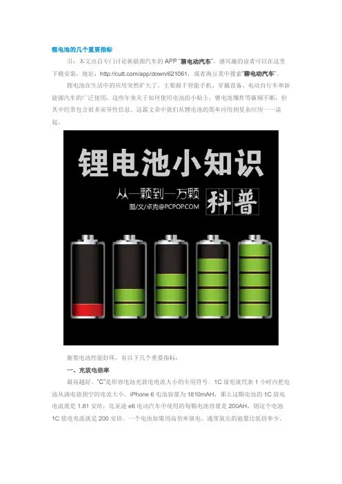
锂电池的几个重要指标引:本文出自专门讨论新能源汽车的APP “聊电动汽车”,感兴趣的读者可以在这里下载安装,地址:/app/down/621061,或者豌豆荚中搜索“聊电动汽车”。
锂电池在生活中的应用突然扩大了,主要源于智能手机、穿戴设备、电动自行车和新能源汽车的广泛使用,这些年来关于如何使用电池的小贴士,锂电池爆炸等新闻不断,但其中经常包含很多误导性信息。
这篇文章中我们从锂电池的简单应用到复杂应用一一说起。
衡量电池性能好坏,有以下几个重要指标:一、充放电倍率最高越好。
“C”是形容电池充放电电流大小的专用符号。
1C放电就代表1小时内把电池从满电放到空的电流大小。
iPhone 6电池容量为1810mAH,那么这颗电池的1C放电电流就是1.81安培;比亚迪e6电动汽车中使用的每颗电池容量是200AH,则这个电池1C 放电电流就是200安培。
一个电池如果用高倍率放电,通常放出的能量比低倍率少。
不同放电倍率下放出的电量从上图测试结果可知这颗动力电池使用10C放电放出的能量只有1C放电下的85%,使用20C放电放出的能量只有1C放电下的70%。
二、充放电循环次数最多越好。
500次是锂电池的常见值,根据不同材料制作的锂电池充放电次数从300-3000次不等。
这个值的具体含义每个工厂可能略有不同,大致可以理解为:按厂商规定的充放电倍率(比如1C放电,0.3C充电;每次从0%充放到100%,照此循环)下,500次循环后,电池容量还剩最初的80%。
充放电次数和使用习惯的关系太大了,我们举几个例子。
1、充放电强度对循环次数的影响工厂标注:每次从0%充放到100%,1C放,0.3C充,500次后容量衰减到80%,这是最严苛的测试循环,也可以不这么严格,看下面如果每次电量的循环都在25%-75%,1C放,0.3C充,2000次后容量衰减到80% 如果每次电量的循环都在50%-100%,1C放,0.3充,1800次后容量衰减到80%2、浅充浅放对寿命的影响工厂标注:每次从0%充放到100%,1C放,0.3C充,500次后容量衰减到80%,是最严苛的测试循环,也可以不这么严格,看下面每次电量的循环都在25%-75%,1C放,0.3C充,2000次后容量衰减到80%每次电量的循环都在50%-100%,1C放,0.3充,1800次后容量衰减到80%以上两个例子可看出充放电的倍率越小、越有利于寿命提升;浅充浅放也有利于寿命提升。
手机锂电池介绍及手机首次充电方法正确知识手机首次充电方法及关于锂电池充电的正确知识首次充电方法及关于手机锂电池充电的知识在手机中,无论是从技术角度评估还是从价格方面的考虑,电池都占有十分重要的地位。
时值今日,市场上正在销售的手机中,所使用的电池已经基本完成了从镍电池到锂电池的过渡。
也许是由于手机电池刚刚完成了一次镍电池到锂电池的革命,所以人们对锂电池的认识并不统一,在许多情况下不正确的说法和做法颇为流行。
因此,懂得一点锂电池的知识,掌握锂电池的正确使用方法是非常有必要的。
1.锂电池的种类目前市面上所使用的二次电池主要有镍氢(Ni-MH)与锂离子(Li-ion)两种类型。
锂离子电池中已经量产的有液体锂离子电池(LiB)和聚合物锂离子电池(LiP)两种。
所以在许多情况下,电池上标注了Li-ion的,一定是锂离子电池。
但不一定就是液体锂离子电池,也有可能是聚合物锂离子电池。
锂离子电池是锂电池的改进型产品。
锂电池很早以前就有了,但锂是一种高度活跃(还记得它在元素周期表中的位置吗?)的金属,它使用时不太安全,经常会在充电时出现燃烧、爆裂的情况,后来就有了改进型的锂离子电池,加入了能抑制锂元素活跃的成份(比如钴、锰等等)从而使锂电真正达到了安全、高效、方便,而老的锂电池也随之基本上淘汰了。
至于如何区分它们,从电池的标识上就能识别,锂电池为Li、锂离子电池为Li-ion。
现在,笔记本和手机使用的所谓“锂电池”,其实都是锂离子电池。
现代电池的基本构造包括正极、负极与电解质三项要素。
作为电池的一种,锂离子电池同样具有这三个要素。
一般锂离子技术使用液体或无机胶体电解液,因此需要坚固的外壳来容纳可燃的活性成分,这就增加了电池的重量和成本,也限制了尺寸大小和造型的灵活性。
一般而言,液体锂离子二次电池的最小厚度是6mm,再减少就比较困难。
而所谓聚合物锂离子电池是在这三种主要构造中至少有一项或一项以上使用高分子材料作为其主要的电池系统。
【LI-ion(新)电池充电常识】【使用小常识】:锂离子电池目前由液态锂离子电池(LIB)和聚合物锂离子电池(PLB)两类。
其中,液态锂离子电池是指Li +嵌入化合物为正、负极的二次电池。
正极采用锂化合物LiCoO2或LiMn2O4,负极采用锂-碳层间化合物。
锂离子电池由于工作电压高、体积小、质量轻、能量高、无记忆效应、无污染、自放电小、循环寿命长,是21世纪发展的理想能源。
1992年锂离子电池开始实用化,使人们的移动电话、笔记本电脑等便携式电子设备重量和体积大大减小。
使用时间大大延长。
由于锂离子电池中不含有重金属镉,与镍镉电池相比,大大减少了对环境的污染。
锂离子电池的特征A.高能量密度锂离子电池的重量是相同容量的镍镉或镍氢电池的一半,体积是镍镉的20-30%,镍氢的35-50%。
B.高电压一个锂离子电池单体的工作电压为 3.7V(平均值),相当于三个串联的镍镉或镍氢电池。
C.无污染锂离子电池不含有诸如镉、铅、汞之类的有害金属物质。
D.不含金属锂锂离子电池不含金属锂,因而不受飞机运输关于禁止在客机携带锂电池等规定的限制。
仅会限制一定的数量。
E.循环寿命高在正常条件下,锂离子电池的充放电周期可超过500次。
F.无记忆效应记忆效应是指镍镉电池在充放电循环过程中,电池的容量减少的现象。
锂离子电池不存在这种效应。
G.快速充电使用额定电压为4.2V的恒流恒压充电器,可以使锂离子电池在1.5--2.5个小时内就充满电;锂离子电池在20℃下可储存半年以上,这是由于它的自放电率很低,而且大部分容量可以恢复。
锂电池存在自放电现象,如果电池电压在3.6V以下长时间保存,会导致电池过放电而破坏电池内部结构,缩短电池寿命。
因此长期保存的锂电池应当每3~6个月补电一次,即充电到电压为3.8~3.9V(锂电池最佳储存电压为3.85V左右)为宜,不宜充满。
锂电池的应用温度范围很广,在北方的冬天室外,仍然可以使用,但容量会降低很多,如果回到室温的条件下,容量又可以恢复。
锂离子电池充电知识(转载)一、基本概念:1、锂离子电池标称电压3.7V(3.6V),充电截止电压4.2V(4.1V,根据电芯的厂牌有不同的设计)。
(锂离子电芯规范的说法是:锂离子二次电池)2、对锂离子电池充电要求(GB/T18287 2000规范):首先恒流充电,即电流一定,而电池电压随着充电过程逐步升高,当电池端电压达到4.2V(4.1V),改恒流充电为恒压充电,即电压一定,电流根据电芯的饱和程度,随着充电过程的继续逐步减小,当减小到0.0 1C时,认为充电终止。
(C是以电池标称容量对照电流的一种表示方法,如电池是1000mAh的容量,1C就是充电电流1000mA,注意是mA而不是mAh,0.01C就是10mA。
)当然,规范的表示方式是0.01C5A,我这里简化了。
3、为什么认为0.01C为充电结束:这是国家标准GB/T18287-2000所规定的,也是讨论得出的。
以前大家普遍以20mA为结束,邮电部行业标准YD/T998-1999也是这样规定的,即不管电池容量多大,停止电流都是20mA。
国标规定的0.01C有助于充电更饱满,对厂家一方通过鉴定有利。
另外,国标规定了充电时间不超过8小时,就是说即使还没有达到0.01C,8小时到了,也认为充电结束。
(质量没问题的电池,都应在8小时内达到0.01 C,质量不好的电池,等下去也无意义),4、怎样区别电池是4.1V还是4.2V:消费者是无法区分的,这要看电芯生产厂家的产品规格书。
有些牌子的电芯是4.1V和4.2V通用的,比如A&TB(东芝),国内厂家基本是4.2V,但也有例外,比如天津力神是4.1V(但目前也是按4.2V了)。
5、把4.1V的电芯充电到4.2V会怎么样:会使电池容量提高,感觉很好用,待机时间增加,但会减短电池的使用寿命。
比如原来500次,减少到300次。
同样道理,把4.2V的电芯过充,也会减短寿命。
锂离子电芯是很娇嫩的。
6、既然电池内有保护板,我们是否就可以放心了呢:不是,因为保护板的截止参数是4.35V(这还是好的,差的要4.4到4.5V),保护板是应付万一的,假如每次都过充,电池也会很快衰减的。