IDT10S60C_rev2[1].1
- 格式:pdf
- 大小:423.01 KB
- 文档页数:7
S60手持式数据采集器用户手册2011年08月前言关于本手册感谢您选择本公司的产品。
本手册可帮助您简单的学会使用本产品。
使用前请通读本手册,并保管好,以便所有使用本产品的人均可阅读。
版权声明本手册内所收录信息及内容为说明产品目前状况,不具保证意涵,包括且不限于任何暗示性或可销售性保证,或适用于某一特殊目的保证;产品以实物为准,本手册内容有可能与实物有所差异,恕不另行通知。
本手册内包含有受版权法保护的独家专利信息,版权所有。
除版权法允许部分,否则未经中山市讯华软件有限公司科技有限公司书面同意,不得影印、重制作、修改或翻译部份或全部内容。
控制本产品的程序部分亦受版权法保护,版权所有,不得侵犯。
Microsoft、ActiveSync、Pocket IE、Pocket Word、Windows、Windows 98、Windows Me、Windows NT、Windows 2000、Windows XP、Windows标志、Windows CE标志或为注册商标,或为Microsoft Corporation在美国及/或其它国家之注册商标。
Microsoft产品为Microsoft Licensing, Inc.授权之OEM产品,Microsoft Licensing, Inc.为Microsoft完全拥有。
本手册内所提及的所有其它品牌名称及产品名称皆为各公司的商标名、服务标志或注册商标。
目录第一章原装配件2第二章产品简介3主要功能特点3产品详细参数4正面(功能介绍)5键盘(功能介绍)错误!未定义书签。
背面(功能介绍)错误!未定义书签。
第三章开始使用8点触操作9更改日期时间10输入文字11扫描条形码14与电脑联机15查看电池电量15校正触摸屏16第四章售后服务181. 支持服务182. 保修期限193. 保修范围19第一章原装配件原装配件您购买的设备包含以下配件主机: 1台电池:2块充电器: 1个数据线: 1条使用手册: 1套合格证: 1套2 / 20质保书: 1本手写笔: 1支防滑背带: 1套注意事项本设备某些功能取决于设备具体配置,请购买时对照配置型号,使用本产品。
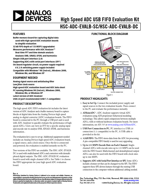
High Speed ADC USB FIFO Evaluation KitHSC-ADC-EVALB-SC/HSC-ADC-EVALB-DC Rev. 0Information furnished by Analog Devices is believed to be accurate and reliable. However, noresponsibility is assumed by Analog Devices for its use, nor for any infringements of patents or other rights of third parties that may result from its use. Specifications subject to change without notice. No license is granted by implication or otherwise under any patent or patent rights of Analog Devices. T rademarks and registered trademarks are the property of their respective owners. One Technology Way, P.O. Box 9106, Norwood, M A 02062-9106, U.S.A. Tel: 781.329.4700 Fax: 781.461.3113 ©2006 Analog Devices, Inc. All rights reserved.FEATURESBuffer memory board for capturing digital dataused with high speed ADC evaluation boardsto simplify evaluation32 kB FIFO depth at 133 MSPS (upgradable)Measures performance with ADC Analyzer™Real-time FFT and time domain analysisAnalyzes SNR, SINAD, SFDR, and harmonicsSimple USB port interface (2.0)Supporting ADCs with serial port interfaces (SPI®)On-board regulator circuit, no power supply required6 V, 2 A switching power supply includedCompatible with Windows® 98 (2nd ed.), Windows 2000, Windows Me, and Windows XPEQUIPMENT NEEDEDAnalog signal source and antialiasing filterLow jitter clock sourceHigh speed ADC evaluation board and ADC data sheetPC running Windows 98 (2nd ed.), Windows 2000,Windows Me, or Windows XPLatest version of ADC AnalyzerUSB 2.0 port recommended (USB 1.1-compatible) PRODUCT DESCRIPTIONThe high speed ADC FIFO evaluation kit includes the latest version of ADC Analyzer and a buffer memory board to capture blocks of digital data from the Analog Devices high speed analog-to-digital converter (ADC) evaluation boards. The FIFO board is connected to the PC through a USB port and is used with ADC Analyzer to quickly evaluate the performance of high speed ADCs. Users can view an FFT for a specific analog input and encode rate to analyze SNR, SINAD, SFDR, and harmonic information.The evaluation kit is easy to set up. Additional equipment needed includes an Analog Devices high speed ADC evaluation board, a signal source, and a clock source. Once the kit is connected and powered, the evaluation is enabled instantly on the PC. Two versions of the FIFO are available. The HSC-ADC-EV ALB-DC is used with multichannel ADCs and converters with demulti-plexed digital outputs. The HSC-ADC-EV ALB-SC evaluation board is used with single-channel ADCs. See Table 1 to choose the FIFO appropriate for your high speed ADC evaluation board.FUNCTIONAL BLOCK DIAGRAM5Figure 1.PRODUCT HIGHLIGHTS1.Easy to Set Up. Connect the included power supply and signal sources to the two evaluation boards. Then connectto the PC and evaluate the performance instantly.2.ADIsimADC™. ADC Analyzer supports virtual ADC evaluation using ADI proprietary behavioral modeling technology. This allows rapid comparison between multiple ADCs, with or without hardware evaluation boards. For more information, see AN-737 at /ADIsimADC.B Port Connection to PC. PC interface is a USB 2.0 connection (1.1-compatible) to the PC. A USB cable is provided in the kit.4.32 kB FIFO. The FIFO stores data from the ADC for processing.A pin-compatible FIFO family is used for easy upgrading.5.Up to 133 MSPS Encode Rate on Each Channel. Single-channel ADCs with encode rates up to 133 MSPS can be used with the FIFO board. Multichannel and demultiplexed output ADCs can also be used with the FIFO board with clock rates up to 266 MSPS.6.Supports ADC with Serial Port Interface or SPI. Some ADCs include a feature set that can be changed via the SPI. The FIFO supports these SPI-driven features through the existing USB connection to the computer without additional cabling needed.HSC-ADC-EVALB-SC/HSC-ADC-EVALB-DCRev. 0 | Page 2 of 28TABLE OF CONTENTSFeatures..............................................................................................1 Equipment Needed...........................................................................1 Product Description.........................................................................1 Functional Block Diagram..............................................................1 Product Highlights...........................................................................1 Revision History...............................................................................2 FIFO Evaluation Board Easy Start..................................................3 Requirements................................................................................3 Easy Start Steps.............................................................................3 Virtual Evaluation Board Easy Start With ADIsimADC............4 Requirements................................................................................4 Easy Start Steps.............................................................................4 FIFO 4.1 Data Capture Board Features.........................................5 FIFO 4.1 Supported ADC Evaluation Boards..........................6 Theory of Operation........................................................................9 Clocking Description...................................................................9 SPI Description.............................................................................9 Clocking with Interleaved Data................................................10 Connecting to the HSC-ADC-FPGA-4/-8.............................10 Connecting to the DEMUX BRD............................................10 Upgrading FIFO Memory.........................................................10 Jumpers............................................................................................11 Default Settings...........................................................................11 Evaluation Board............................................................................13 Power Supplies............................................................................13 Connection and Setup...............................................................13 FIFO Schematics and PCB Layout...............................................14 Schematics...................................................................................14 PCB Layout.................................................................................21 Bill of Materials...............................................................................23 Ordering Information....................................................................25 Ordering Guide..........................................................................25 ESD Caution.. (25)REVISION HISTORY2/06—Revision 0: Initial VersionHSC-ADC-EVALB-SC/HSC-ADC-EVALB-DCRev. 0 | Page 3 of 28FIFO EVALUATION BOARD EASY STARTREQUIREMENTS• FIFO evaluation board, ADC Analyzer, and USB cable • High speed ADC evaluation board and ADC data sheet • Power supply for ADC evaluation board • Analog signal source and appropriate filtering • Low jitter clock source applicable for specific ADC evaluation, typically <1 ps rms• PC running Windows 98 (2nd ed.), Windows 2000, Windows Me, or Windows XP•PC with a USB 2.0 port recommended (USB 1.1-compatible)EASY START STEPSNote: Y ou need administrative rights for the Windows operating systems during the entire easy start procedure. It is recommended to complete every step before reverting to a normal user mode.1. Install ADC Analyzer from the CD provided in the FIFOevaluation kit or download the latest version on the Web. For the latest updates to the software, check the Analog Devices website at /hsc-FIFO . 2. Connect the FIFO evaluation board to the ADC evaluationboard. If an adapter is required, insert the adapter between the ADC evaluation board and the FIFO board. If using the HSC-ADC-EV ALB-SC model, connect the evaluation board to the bottom two rows of the 120-pin connector, closest to the installed IDT FIFO chip. If using an ADC with a SPI interface, remove the two 4-pin corner keys so that the third row can be connected. 3. Connect the provided USB cable to the FIFO evaluationboard and to an available USB port on the computer. 4. Refer to Table 5 for any jumper changes. Most evaluationboards can be used with the default settings. 5. After verification, connect the appropriate power suppliesto the ADC evaluation boards. The FIFO evaluation board is supplied with a wall mount switching power supply that provides a 6 V , 2 A maximum output. Connect the supply end to the rated 100 ac to 240 ac wall outlet at 47 Hz to 63 Hz. The other end is a 2.1 mm inner diameter jack that connects to the PCB at J301. Refer to the instructions included in the ADC data sheet for more information about the ADC evaluation board’s power supply and other requirements. 6. Once the cable is connected to both the computer and theFIFO board, and power is supplied, the USB drivers start to install. To complete the total installation of the FIFO drivers, you need to complete the new hardware sequence two times. The first Found New Hardware Wizard opens with the text message This wizard helps you install software for…Pre-FIFO 4.1. Click the recommended install, and go to the next screen. A hardware installation warning window should then be displayed. Click Continue Anyway . The next window that opens should finish the Pre-FIFO 4.1 installation. Click Finish . Y our computer should go through a second Found New Hardware Wizard , and the text message, This wizard helps you install software for…Analog Devices FIFO 4.1, should be displayed. Continue as you did in the previous installation and click Continue Anyway . Then click Finish on the next two windows. This completes the installation. 7. (Optional) Verify in the device manager that AnalogDevices, FIFO4.1 is listed under the USB hardware. 8. Apply power to the evaluation board and check the voltagelevels at the board level. 9. Connect the appropriate analog input (which should befiltered with a band-pass filter) and low jitter clock signal. Make sure the evaluation boards are powered on before connecting the analog input and clock. 10. Start ADC Analyzer.11. Choose an existing configuration file for the ADCevaluation board or create one. 12. Click Time Data in ADC Analyzer (left-most button underthe menus). A reconstruction of the analog input isdisplayed. If the expected signal does not appear, or if there is only a flat red line, refer to the ADC Analyzer data sheet at /hsc-FIFO for more information.HSC-ADC-EVALB-SC/HSC-ADC-EVALB-DCRev. 0 | Page 4 of 28VIRTUAL EVALUATION BOARD EASY START WITH ADIsimADCREQUIREMENTSRequirements include • Completed installation of ADC Analyzer, Version 4.5.17 or later.•ADIsimADC product model files for the desired converter. Models are not installed with the software, but they can be downloaded from the ADIsimADC Virtual Evaluation Board website at no charge.No hardware is required. However, if you wish to compareresults of a real evaluation board and the model, you can switch easily between the two, as outlined in the following Easy Start Steps section.EASY START STEPS1. To get ADC model files, go to /ADIsimADCfor the product of interest. Download the product ofinterest to a local drive. The default location is c:\program files\adc_analyzer\models. 2. Start ADC Analyzer (see the ADC Analyzer User Manual ). 3. From the menu, click Config > Buffer > Model as thebuffer memory. In effect, the model functions in place of the ADC and data capture hardware. 4. After selecting the model, click the Model button (locatednext to the Stop button) to select and configure which converter is to be modeled. A dialog box appears in the workspace, where you can select and configure the behavior of the model. 5. In the ADC Modeling dialog box, click the Device tab andthen click the … (Browse) button, adjacent to the dialog box. This opens a file browser and displays all of the models found in the default directory: c:\program files\adc_analyzer\models. If no model files are found, follow the on-screen directions or see Step 1 to install available models. If you have saved the models somewhere other than the default location, use the browser to navigate to that location and select the file of interest. 6. From the menu, click Config > FFT . In the FFTConfiguration dialog box, ensure that the EncodeFrequency is set for a valid rate for the simulated device under test. If set too low or too high, the model does not run. 7. Once a model has been selected, information about themodel displays on the Device tab of the ADC Modeling dialog box. After ensuring that you have selected the right model, click the Input tab. This lets you configure the input to the model. Click either Sine Wave or Two Tone for the input signal. 8. Click Time Data (left-most button under the pull-downmenus). A reconstruction of the analog input is displayed . The model can now be used just as a standard evaluation board would be. 9. The model supports additional features not found whentesting a standard evaluation board. When using the modeling capabilities, it is possible to sweep either the analog amplitude or the analog frequency. For more information consult the ADC Analyzer User Manual at /hsc-FIFO .HSC-ADC-EVALB-SC/HSC-ADC-EVALB-DCRev. 0 | Page 5 of 28FIFO 4.1 DATA CAPTURE BOARD FEATURES6V SWITCHING POWER SUPPLY CONNECTIONON BOARD +3.3V REGULATOROPTIONAL POWER CONNECTIONUSB CONNECTION TO COMPUTERµCONTROLLER CRYSTALCLOCK = 24MHz,OFF DURING DATA CAPTURERESET SWITCH WHEN ENCODE RATE IS INTERRUPTEDOPTIONAL SERIAL PORT INTERFACE CONNECTOR OPEN SOLDER MASKON ALL DATA AND CLOCK LINES FOREASY PROBINGIDT72V283 32k ⋅16-BIT 133MHz FIFO120-CONNECTOR (PARALLEL CMOSINPUTS)TIMING ADJUSTMENTJUMPERSIDT72V283 32k ⋅16-BIT 133MHz FIFO05870-002Figure 2. FIFO Components (Top View)HSC-ADC-EVALB-SC/HSC-ADC-EVALB-DCRev. 0 | Page 6 of 28120-CONNECTOR (PARALLEL CMOS INPUTS)TIMING ADJUSTMENT JUMPERSDRIVER CIRCUIT FORSERIAL PORT INTERFACE (SPI) LINESOPTIONAL SERIAL PORT INTERFACE (SPI) CONNECTORCYPRESS Fx2 HIGH SPEED USB 2.0 µCONTROLLEREPROM TO LOAD USB FIRMWARE05870-003Figure 3. FIFO Components (Bottom View)FIFO 4.1 SUPPORTED ADC EVALUATION BOARDSThe evaluation boards in Table 1 can be used with the high speed ADC FIFO evaluation kit. Some evaluation boards require an adapter between the ADC evaluation board connector and the FIFO connector . If an adapter is needed, send an email to highspeed.converters@ with the part number of the adapter and a mailing address.Table 1. HSC-ADC-EVALB-DC- and HSC-ADC-EVALB-SC-Compatible Evaluation Boards 1Evaluation Board Model Description of ADC FIFO Board Version Comments AD6644ST/PCB 14-bit, 65 MSPS ADC SC AD6645-80/PCB 14-bit, 80 MSPS ADC SC AD6645-105/PCB 14-bit, 105 MSPS ADC SC AD9051/PCB10-bit, 60 MSPS ADC SC Requires AD9051FFA AD9200SSOP-EVAL 10-bit, 20 MSPS ADC SC Requires AD922xFFA AD9200TQFP-EVAL 10-bit, 20 MSPS ADCSC Requires AD922xFFAAD9201-EVAL Dual 10-bit, 20 MSPS ADC 1SC Requires AD922xFFA AD9203-EB 10-bit, 40 MSPS ADCSC Requires AD922xFFA AD9212-65EB 1Octal 10-bit, 65 MSPS ADC DC Requires HSC-ADC-FPGA-8 AD9215BCP-65EB 10-bit, 65 MSPS ADC SC AD9215BCP-80EB 10-bit, 80 MSPS ADC SC AD9215BCP-105EB 10-bit, 105 MSPS ADC SC AD9215BRU-65EB 10-bit, 65 MSPS ADC SC AD9215BRU-80EB 10-bit, 80 MSPS ADC SC AD9215BRU-105EB 10-bit, 105 MSPS ADC SC AD9216-80PCB Dual 10-bit, 80 MSPS ADC DCAD9216-105PCBDual 10-bit, 105 MSPS ADCDCHSC-ADC-EVALB-SC/HSC-ADC-EVALB-DCRev. 0 | Page 7 of 28Evaluation Board Model Description of ADC FIFO Board Version Comments AD9218-105PCB 10-bit, 105 MSPS ADC DC AD9218-65PCB 10-bit, 65 MSPS ADC DCAD9219-65EB 1Quad 10-bit, 65 MSPS ADC DC Requires HSC-ADC-FPGA-4/-8 AD9220-EB 12-bit, 10 MSPS ADC SC Requires AD922xFFA AD9222-65EB 1Octal 12-bit, 65 MSPS ADC DC Requires HSC-ADC-FPGA-8 AD9226-EB 12-bit, 65 MSPS ADC SC Requires AD922xFFA AD9226QFP-EB 12-bit, 65 MSPS ADC SC Requires AD922xFFA AD9228-65EB 1Quad 12-bit, 65 MSPS ADC DC Requires HSC-ADC-FPGA-4/-8AD9229-65EB 1Quad 12-bit, 65 MSPS ADC DC Requires HSC-ADC-FPGA-4/-8 AD9233-80EB 12-bit, 80MSPS ADC SC AD9233-105EB 12-bit, 105MSPS ADC SC AD9233-125EB 12-bit, 125MSPS ADC SC AD9234-EB 12-bit, 150MSPS ADC SC AD9235BCP-20EB 12-bit, 20 MSPS ADC SC AD9235BCP-40EB 12-bit, 40 MSPS ADC SC AD9235BCP-65EB 12-bit, 65 MSPS ADC SC AD9235-20PCB 12-bit, 20 MSPS ADC SC AD9235-40PCB 12-bit, 40 MSPS ADC SC AD9235-65PCB 12-bit, 65 MSPS ADC SC AD9236BRU-80EB 12-bit, 80 MSPS ADC SC AD9236BCP-80EB 12-bit, 80 MSPS ADC SC AD9237BCP-20EB 12-bit, 20 MSPS ADC SC AD9237BCP-40EB 12-bit, 40 MSPS ADC SCAD9237BCP-65EB 12-bit, 65 MSPS ADC SCAD9238BST-20PCB Dual 12-bit, 20 MSPS ADC DC AD9238BST-40PCB Dual 12-bit, 40 MSPS ADC DC AD9238BST-65PCB Dual 12-bit, 65 MSPS ADC DC AD9238BCP-20EB Dual 12-bit, 20 MSPS ADC DC AD9238BCP-40EB Dual 12-bit, 40 MSPS ADC DC AD9238BCP-65EB Dual 12-bit, 65 MSPS ADC DC AD9240-EB 14-bit, 40 MSPS ADC SC Requires AD922xFFA AD9241-EB 14-bit, 1.25 MSPS ADC SC Requires AD922xFFA AD9243-EB 14-bit, 3 MSPS ADC SC Requires AD922xFFA AD9244-40PCB 14-bit, 40 MSPS ADC SC AD9244-65PCB 14-bit, 65 MSPS ADC SCAD9245BCP-20EB 14-bit, 20 MSPS ADCSC AD9245BCP-40EB 14-bit, 40 MSPS ADCSC AD9245BCP-65EB 14-bit, 65 MSPS ADCSC AD9245BCP-80EB 14-bit, 80 MSPS ADCSC AD9246-80EB 14-bit, 80 MSPS ADCSC AD9246-105EB 14-bit, 105 MSPS ADCSC AD9246-125EB 14-bit, 125 MSPS ADCSC AD9248BST-65EB Dual 14-bit, 65 MSPS ADC DC AD9248BCP-20EB Dual 14-bit, 20 MSPS ADC DC AD9248BCP-40EB Dual 14-bit, 40 MSPS ADC DC AD9248BCP-65EB Dual 14-bit, 65 MSPS ADC DCAD9259-50EB 1Quad 14-bit, 50 MSPS ADC DC Requires HSC-ADC-FPGA-4/-8 AD9260-EB 16-bit, 2.5 MSPS ADC SC Requires AD922xFFA AD9280-EB 8-bit, 32 MSPS ADC SC Requires AD922xFFA AD9281-EB Dual 8-bit, 28 MSPS ADC SC Requires AD922xFFA AD9283/PCB 8-bit, 100 MSPS ADC SC Requires AD9283FFAAD9287-100EB 1Quad 8-bit, 100 MSPS ADC DC Requires HSC-ADC-FPGA-4/-8AD9289-65EB 1Quad 8-bit, 65 MSPS ADC DC Requires HSC-ADC-FPGA-9289 AD9411/PCB 10-bit, 200 MSPS ADC DC Requires DEMUX BRDHSC-ADC-EVALB-SC/HSC-ADC-EVALB-DCEvaluation Board Model Description of ADC FIFO Board Version CommentsAD9430-CMOS/PCB 12-bit, 210 MSPS ADC DCAD9430-LVDS/PCB212-bit, 210 MSPS ADC DC Requires DEMUX BRDAD9432/PCB 12-bit, 105 MSPS ADC SCAD9433/PCB 12-bit, 125 MSPS ADC SCAD9444-CMOS/PCB 14 bit, 80 MSPS ADC SCAD9444-LVDS/PCB 14 bit, 80 MSPS ADC SCAD9445-IF-LVDS/PCB 14-bit, 125 MSPS ADC SCAD9445-BB-LVDS/PCB 14-bit, 125 MSPS ADC SCAD9446-80LVDS/PCB 16-bit, 80 MSPS ADC SCAD9446-100LVDS/PCB 16-bit, 100 MSPS ADC SCAD9460-80EB-IF 16-bit, 80 MSPS ADC SCAD9460-80EB-BB 16-bit, 80 MSPS ADC SCAD9460-105EB-IF 16-bit, 105 MSPS ADC SCAD9460-105EB-BB 16-bit, 105 MSPS ADC SCAD9461-130EB-IF 16-bit, 130 MSPS ADC SCAD9461-130EB-BB 16-bit, 130 MSPS ADC SCAD9480-LVDS/PCB28-bit, 250 MSPS ADC DC Requires DEMUX BRDAD9481-PCB 8-bit, 250 MSPS ADC DCAD10200/PCB Dual 12-bit, 105 MSPS ADC DC Requires GS09066AD10201/PCB Dual 12-bit, 105 MSPS ADC DC Requires GS09066AD10226/PCB Dual 12-bit, 125 MSPS ADC DC Requires GS09066AD10265/PCB Dual 12-bit, 65 MSPS ADC DC Requires GS09066AD10465/PCB Dual 14-bit, 65 MSPS ADC DC Requires GS09066AD10677/PCB 16-bit, 65 MSPS ADC SC Requires GS09066AD10678/PCB 16-bit, 80 MSPS ADC SC Requires GS09066AD15252/PCB 12-bit, Dual 65 MSPS ADC DCAD15452/PCB 12-bit, Quad 65 MSPS ADC DC Requires HSC-ADC-FPGA-4/-81 The high speed ADC FIFO evaluation kit can be used to evaluate two channels at a time.2 If a DEMUX BRD is needed, send an email to highspeed.converters@.Rev. 0 | Page 8 of 28HSC-ADC-EVALB-SC/HSC-ADC-EVALB-DCRev. 0 | Page 9 of 28THEORY OF OPERATIONThe FIFO evaluation board can be divided into several circuits, each of which plays an important part in acquiring digital data from the ADC and allows the PC to upload and process that data. The evaluation kit is based around the IDT72V283 FIFO chip from Integrated Device Technology, Inc (IDT). The system can acquire digital data at speeds up to 133 MSPS and data record lengths up to 32 kB using the HSC-ADC-EV ALB-SC FIFO evaluation kit. The HSC-ADC-EVALB-DC, which has two FIFO chips, is available to evaluate multichannel ADCs or demultiplexed data from ADCs sampling faster than 133 MSPS. A USB 2.0 microcontroller communicating with ADC Analyzer allows for easy interfacing to newer computers using the USB 2.0 (USB 1.1-compatible) interface.The process of filling the FIFO chip or chips and reading the data back requires several steps. First, ADC Analyzer initiates the FIFO chip fill process. The FIFO chips are reset, using a master reset signal (MRS). The USB microcontroller is then suspended, which turns off the USB oscillator and ensures that it does not add noise to the ADC input. After the FIFO chips completely fill, the full flags from the FIFO chips send a signal to the USB microcontroller to wake up the microcontroller from suspend. ADC Analyzer waits for approximately 30 ms and then begins the readback process.During the readback process, the acquisition of data from FIFO 1 (U201) or FIFO 2 (U101) is controlled via Signal OEA and Signal OEB. Because the data outputs of both FIFO chips drive the same 16-bit data bus, the USB microcontrollercontrols the OEA and OEB signals to read data from the correct FIFO chip. From an application standpoint, ADC Analyzer sends commands to the USB microcontroller to initiate a read from the correct FIFO chip, or from both FIFO chips in dual or demultiplexed mode.CLOCKING DESCRIPTIONEach channel of the buffer memory requires a clock signal to capture data. These clock signals are normally provided by the ADC evaluation board and are passed along with the data through Connector J104 (Pin 37 for both Channel A and Channel B). If only a single clock is passed for both channels, they can be connected together by Jumper J303.Jumpers J304 and J305 at the output of the LVDS receiver allow the output clock to be inverted by the LVDS receiver. By default, the clock outputs are inverted by the LVDS receiver.The single-ended clock signal from each data channel is buffered and converted to a differential CMOS signal by two gates of a low voltage differential signal (LVDS) receiver, U301. This allows the clock source for each channel to be CMOS, TTL, or ECL. The clock signals are ac-coupled by 0.1 μF capacitors.Potentiometer R312 and Potentiometer R315 allow for fine tuning the threshold of the LVDS gates. In applications where fine-tuning the threshold is critical, these potentiometers can be replaced with a higher resistance value to increase theadjustment range. Resistors R301, R302, R303, R304, R311, R313, R314, and R316 set the static input to each of the differential gates to a dc voltage of approximately 1.5 V . At assembly, Solder Jumper J310 to Solder Jumper J313 are set to bypass the potentiometer. For fine adjustment using the pot, the solder jumpers must be removed, and R312 and R315 must be populated.U302, an XOR gate array, is included in the design to let users add gate delays to the FIFO memory chip clock paths. They are not required under normal conditions and are bypassed at assembly by Jumper J314 and Jumper J315. Jumper J306 and Jumper J307 allow the clock signals to be inverted through an XOR gate. In the default setting, the clocks are not inverted by the XOR gate.The clock paths described above determine the WRT_CLK1 and WRT_CLK2 signals at each FIFO memory chip (U101 and U201). The timing options above should let you choose a clock signal that meets the setup and hold time requirements to capture valid data.A clock generator can be applied directly to S1 and/or S3. This clock generator should be the same unit that provides the clock for the ADC. These clock paths are ac-coupled, so that a sine wave generator can be used. DC bias can be adjusted by R301/R302 and R303/R304.The DS90LV048A differential line receiver is used to square the clock signal levels applied externally to the FIFO evaluation board. The output of this clock receiver can either directly drive the write clock of the IDT72V283 FIFO(s), or first pass through the XOR gate timing circuitry described above.SPI DESCRIPTIONThe Cypress IC (U502) supports the HSC SPI standard to allow programming of ADCs that have SPI-accessible register maps. U102 is a buffer that drives the 4-wire SPI (SCLK, SDI, SDO, CSB 1) through the 120-pin connector (J104) on the third or top row. J502 is an auxiliary SPI connector to monitor the SPI signals connected directly to the Cypress IC. For more information on this and other functions, consult the user manual titled Interfacing to High Speed ADCs via SPI at /hsc-FIFO .1Note that CSB1 is the default CSB line used.HSC-ADC-EVALB-SC/HSC-ADC-EVALB-DCRev. 0 | Page 10 of 28The SPI interface designed on the Cypress IC can communicate with up to five different SPI-enabled devices. The CLK and data lines are common to all SPI devices. The correct device ischosen to communicate by using one of the five active low chip select pins. This functionality is controlled by selecting a SPI channel in the software.CLOCKING WITH INTERLEAVED DATAADCs with very high data rates can exceed the capability of a single buffer memory channel (~133 MSPS). These converters often demultiplex the data into two channels to reduce the rate required to capture the data. In these applications, ADC Analyzer must interleave the data from both channels to process it as a single channel. The user can configure the software to process the first sample from Channel A, the second from Channel B, and so on, or vice versa. The synchronization circuit included in the buffer memory forces a small delay between the write enable signals (WENA and WENB) to the FIFO memory chips (Pin 1, U101, and U201), ensuring that the data is captured in one FIFO before the other. Jumper J401 and Jumper J402 determine which FIFO receives WENA and which FIFO receives WENB.CONNECTING TO THE HSC-ADC-FPGA-4/-8ADCs that have serial LVDS outputs require another board that is connected between the ADC evaluation board and the FIFO data capture card. This board converts the serial data into parallel CMOS so that the FIFO data capture card can accept the data. For more detailed information on this board, refer to the HSC-ADC-FPGA datasheet at /hsc-FIFO . CONNECTING TO THE DEMUX BRDADCs that have parallel LVDS outputs require another board that is connected between the ADC evaluation board and the FIFO data capture card. This board converts parallel LVDS to parallel CMOS, using both channels of the FIFO data capture card. For more detailed information on this board, send an email to highspeed.converters@UPGRADING FIFO MEMORYThe FIFO evaluation board includes one or two 32 kB FIFOs that are capable of 133 MHz clock signals, depending on the model number. Pin-compatible FIFO upgrades are available from IDT. See Table 2 for the IDT part number matrix.Table 2. IDT Part Number MatrixPart NumberFIFO Depth FIFO Speed IDT72V283-L7-5PF (Default ) 32 kB 133 MHz IDT72V293-L7-5PF 64 kB 133 MHz IDT72V2103-L7-5PF 132 kB 133 MHz IDT72V2113-L7-5PF 256 kB 133 MHz IDT72V283-L6PF 32 kB 166 MHz IDT72V293-L6PF 64 kB 166 MHz IDT72V2103-L6PF 132 kB 166 MHz IDT72V2113-L6PF256 kB166 MHzFor more information, visit .。


回馈式源载系统IT6000B系列用户手册型号:IT6000B系列版本:V1.3/06,2020声明©Itech Electronic,Co.,Ltd. 2020根据国际版权法,未经Itech Electronic,Co.,Ltd.事先允许和书面同意,不得以任何形式(包括电子存储和检索或翻译为其他国家或地区语言)复制本手册中的任何内容。
手册部件号商标声明Pentium是Intel Corporation 在美国的注册商标。
Microsoft、Visual Studio、Windows和MS Windows是Microsoft Corporation在美国和/或其他国家/地区的商标。
担保本文档中包含的材料“按现状”提供,在将来版本中如有更改,恕不另行通知。
此外,在适用法律允许的最大范围内,ITECH不承诺与本手册及其包含的任何信息相关的任何明示或暗含的保证,包括但不限于对适销和适用于某种特定用途的暗含保证。
ITECH对提供、使用或应用本文档及其包含的任何信息所引起的错误或偶发或间接损失概不负责。
如ITECH与用户之间存在其他书面协议含有与本文档材料中所包含条款冲突的保证条款,以其他书面协议中的条款为准。
技术许可本文档中描述的硬件和/或软件仅在得到许可的情况下提供并且只能根据许可进行使用或复制。
限制性权限声明美国政府限制性权限。
授权美国政府使用的软件和技术数据权限仅包括那些定制提供给最终用户的权限。
ITECH在软件和技术数据中提供本定制商业许可时遵循FAR12.211(技术数据)和12.212(计算机软件)以及用于国防的DFARS252.227-7015(技术数据-商业制品)和DFARS227.7202-3(商业计算机软件或计算机软件文档中的权限)。
安全声明“小心”标志表示有危险。
它要求在执行操作步骤时必须加以注意,如果不正确地执行或不遵守操作步骤,则可能导致产品损坏或重要数据丢失。
在没有完全理解指定的条件且不满足这些条件的情况下,请勿继续执行小心标志所指示的任何不当操作。
Transistors Rev.A 1/2Power Transistor (−100V , −2A)2SB1580 / 2SB1316z Features1) Darlington connection for high DC current gain. 2) Built-in resistor between base and emitter. 3) Built-in damper diode.4) Complements the 2SD2195 / 2SD1980.z Absolute maximum ratings (T a = 25°C)ParameterSymbol V CBO V CEO V EBOI CP C TjTstg Limits −100−100−8−221150−55 to +150Unit V V V A(DC)−3∗1A(Pulse)W 10∗2W(Tc =25°C)2SB15802SB1316°CCollector-base voltage Collector-emitter voltage Emitter-base voltage Collector currentCollectorpowerdissipationJunction temperature Storage temperature°C ∗1 Single pulse Pw =100ms∗2 When mounted on a 40 x 40 x 0.7 mm ceramic board.z Packaging specifications and h FEType 2SB1580MPT31k to 10k T1001000BN ∗2SB1316CPT31k to 10kTL 2500−Denotes h FEPackage h FECodeBasic ordering unit (pieces)Marking ∗z Equivalent circuitz External dimensions (Unit : mm)2SB13162SB1580(3) Emitter(2) Collector (1) Base EIAJ : SC-62(3) Emitter(2) Collector (1) Base ROHM : CPT3EIAJ : SC-631.50.41.50.41.60.53.00.41.5(3)4.5(1)(2)0.54.02.51.0ROHM : MPT32.30.51.00.59.52.50.8Min.1.56.52.3(2)(3)C0.50.650.9(1)0.752.30.91.55.55.1z Electrical characteristics (T a = 25°C)ParameterSymbol Min.Typ.Max.Unit ConditionsBV CBO BV CEO I CBO I EBO Cob−100−100−−−−−−−35−−−10−3−V V µA mA pF MHz I C = −50µA I C = −5mA V CB = −100V V EB = −7VV CE(sat)−−−1.5V I C /I B = −1A/−1mA h FE 1000−10000−∗V CE = −2V , I C = −1AV CB = −10V , I E = 0A , f = 1MHzCollector-base breakdown voltage Collector-emitter breakdown voltage BV EBO −10−−V I E = −5mA Emitter-base breakdown voltage Collector cutoff current Emitter cutoff currentOutput capacitanceCollector-emitter saturation voltage DC current transfer ratio f T 50−−V CE = −5V , I E =0.1A , f = 30MHz Transition frequency ∗∗Transistors Rev.A2/2z Electrical characteristics curveBASE TO EMITTER VOLTAGE : V BE (V)C O L L E C T O R C U R R E N T : I C (A )Fig.2 Grounded emitter propagation characteristics−−−−−−−−−−C O L L E C T O R C U R R E N T : IC (A )COLLECTOR TO EMITTER VOLTAGE : V CE (V)Fig.1 Grounded emitter output characteristics−−−−−COLLECTOR CURRENT : I C (A)D C C U R RE N T G A I N : h E FFig.3 DC current gain vs. collector current−COLLECTOR CURRENT : I C (A)C O L L E CT O R S A T U R A T I O N V O L T A G E : V C E (s a t ) (V )Fig.4 Collector-emitter saturation voltage vs. collector current −−−−−−−−−−COLLECTOR TO BASE VOLTAGE : V CB (V)C O L L E C T O R O U T P U T C A P A C I T A N C E : C o b (p F )Fig.5 Collector output capacitance vs. collector-base voltageFig.6 Safe Operating area (2SB1580)COLLECTOR TO EMITTER VOLTAGE : V CE (V)C O L L E C T O R C U R R E N T : I C (A )Fig.7 Safe Operating area (2SB1316)COLLECTOR TO EMITTER VOLTAGE : V CE (V)C O L L E C T O R C U R R E N T : I C (A )AppendixAbout Export Control Order in JapanProducts described herein are the objects of controlled goods in Annex 1 (Item 16) of Export T rade ControlOrder in Japan.In case of export from Japan, please confirm if it applies to "objective" criteria or an "informed" (by MITI clause)on the basis of "catch all controls for Non-Proliferation of Weapons of Mass Destruction.Appendix1-Rev1.1。
Dimensions: [mm]11Scale - 10:11541141NAA5701541141NAA5701541141NAA5701541141NAA5701541141NAA570T e m p e r a t u r eT pT L1541141NAA570Cautions and Warnings:The following conditions apply to all goods within the product series of Optoelectronic Components of Würth Elektronik eiSos GmbH & Co. KG:General:•This optoelectronic component is designed and manufactured for use in general electronic equipment.•Würth Elektronik must be asked for written approval (following the PPAP procedure) before incorporating the components into any equipment in fields such as military, aerospace, aviation, nuclear control, submarine, transportation (automotive control, train control, ship control), transportation signal, disaster prevention, medical, public information network, etc. where higher safety and reliability are especially required and/or if there is the possibility of direct damage or human injury.•Optoelectronic components that will be used in safety-critical or high-reliability applications, should be pre-evaluated by the customer. •The optoelectronic component is designed and manufactured to be used within the datasheet specified values. If the usage and operation conditions specified in the datasheet are not met, the wire insulation may be damaged or dissolved.•Do not drop or impact the components, the component may be damaged.•Würth Elektronik products are qualified according to international standards, which are listed in each product reliability report. Würth Elektronik does not warrant any customer qualified product characteristics beyond Würth Elektroniks’ specifications, for its validity and sustainability over time.•The responsibility for the applicability of the customer specific products and use in a particular customer design is always within the authority of the customer. All technical specifications for standard products also apply to customer specific products.•Unless Würth Elektroik has given its express consent, the customer is under no circumstances entitled to reverse engineer, disassemble or otherwise attempt to extract knowledge or design information from the optoelectronic component.Product specific:Soldering:•The solder profile must comply with the technical product specifications. All other profiles will void the warranty.•All other soldering methods are at the customers’ own risk.•The soldering pad pattern shown above is a general recommendation for the easy assembly of the optoelectronic component. If a high degree of precision is required for the selected application (i.e. high density assembly), the customer must ensure that the soldering pad pattern is optimized accordingly.Cleaning and Washing:•Washing agents used during the production to clean the customer application might damage or change the characteristics of the optoelectronic component body, marking or plating. Washing agents may have a negative effect on the long-term functionality of the product. •Using a brush during the cleaning process may break the optoelectronic component body. Therefore, we do not recommend using a brush during the PCB cleaning process.Potting:•If the product is potted in the customer application, the potting material might shrink or expand during and after hardening. Shrinking could lead to an incomplete seal, allowing contaminants into the optoelectronic component body, pins or termination. Expansion could damage the components. We recommend a manual inspection after potting to avoid these effects.Storage Conditions:• A storage of Würth Elektronik products for longer than 12 months is not recommended. Within other effects, the terminals may suffer degradation, resulting in bad solderability. Therefore, all products shall be used within the period of 12 months based on the day of shipment.•Do not expose the optoelectronic component to direct sunlight.•The storage conditions in the original packaging are defined according to DIN EN 61760-2.•For a moisture sensitive component, the storage condition in the original packaging is defined according to IPC/JEDEC-J-STD-033. It is also recommended to return the optoelectronic component to the original moisture proof bag and reseal the moisture proof bag again. •The storage conditions stated in the original packaging apply to the storage time and not to the transportation time of the components. Handling:•Violation of the technical product specifications such as exceeding the nominal rated current, will void the warranty.•The product design may influence the automatic optical inspection.•Certain optoelectronic component surfaces consist of soft material. Pressure on the top surface has to be handled carefully to prevent negative influence to the function and reliability of the optoelectronic components.•ESD prevention methods need to be applied for manual handling and processing by machinery.•Resistors for protection are obligatory.•Luminaires in operation may harm human vision or skin on a photo-biological level. Therefore direct light impact shall be avoided. •In addition to optoelectronic components testing, products incorporating these devices have to comply with the safety precautions given in IEC 60825-1, IEC 62471 and IEC 62778.•Please be aware that Products provided in bulk packaging may get bent and might lead to derivations from the mechanical manufacturing tolerances mentioned in our datasheet, which is not considered to be a material defect.Technical specification:•The typical and/or calculated values and graphics of technical parameters can only reflect statistical figures. The actual parameters of each single product, may differ from the typical and/or calculated values or the typical characteristic line.•In the characteristics curves, all values given in dotted lines may show a higher deviation than the paramters mentioned above.•On each reel, only one bin is sorted and taped. The bin is defined by the photocurrent.Würth Elektronik eiSos GmbH & Co. KGEMC & Inductive SolutionsMax-Eyth-Str. 174638 WaldenburgGermanyCHECKED REVISION DATE (YYYY-MM-DD)GENERAL TOLERANCE PROJECTIONMETHODSV002.0002022-05-02DIN ISO 2768-1mDESCRIPTIONWL-STSW SMT PhototransistorSideview Waterclear ORDER CODE1541141NAA570SIZE/TYPE BUSINESS UNIT STATUS PAGE•In order to ensure highest availability, the reel binning of standard deliveries can vary. A single bin cannot be ordered. Please contact us in advance, if you need a particular bin sorting before placing your order.These cautions and warnings comply with the state of the scientific and technical knowledge and are believed to be accurate and reliable.However, no responsibility is assumed for inaccuracies or incompleteness.The customer has the sole responsibility to ensure that he uses the latest version of this datasheet, which is available on Würth Elektronik’s homepage. Unless otherwise agreed in writing (i.e. customer specific specification), changes to the content of this datasheet may occurwithout notice, provided that the changes do not have a significant effect on the usability of the optoelectronic components.Würth Elektronik eiSos GmbH & Co. KG EMC & Inductive Solutions Max-Eyth-Str. 174638 Waldenburg GermanyCHECKED REVISION DATE (YYYY-MM-DD)GENERAL TOLERANCEPROJECTION METHODSV002.0002022-05-02DIN ISO 2768-1mDESCRIPTIONWL-STSW SMT Phototransistor Sideview WaterclearORDER CODE1541141NAA570SIZE/TYPEBUSINESS UNITSTATUSPAGEImportant NotesThe following conditions apply to all goods within the product range of Würth Elektronik eiSos GmbH & Co. KG:1. General Customer ResponsibilitySome goods within the product range of Würth Elektronik eiSos GmbH & Co. KG contain statements regarding general suitability for certain application areas. These statements about suitability are based on our knowledge and experience of typical requirements concerning the areas, serve as general guidance and cannot be estimated as binding statements about the suitability for a customer application. The responsibility for the applicability and use in a particular customer design is always solely within the authority of the customer. Due to this fact it is up to the customer to evaluate, where appropriate to investigate and decide whether the device with the specific product characteristics described in the product specification is valid and suitable for the respective customer application or not.2. Customer Responsibility related to Specific, in particular Safety-Relevant ApplicationsIt has to be clearly pointed out that the possibility of a malfunction of electronic components or failure before the end of the usual lifetime cannot be completely eliminated in the current state of the art, even if the products are operated within the range of the specifications.In certain customer applications requiring a very high level of safety and especially in customer applications in which the malfunction or failure of an electronic component could endanger human life or health it must be ensured by most advanced technological aid of suitable design of the customer application that no injury or damage is caused to third parties in the event of malfunction or failure of an electronic component. Therefore, customer is cautioned to verify that data sheets are current before placing orders. The current data sheets can be downloaded at .3. Best Care and AttentionAny product-specific notes, cautions and warnings must be strictly observed. Any disregard will result in the loss of warranty.4. Customer Support for Product SpecificationsSome products within the product range may contain substances which are subject to restrictions in certain jurisdictions in order to serve specific technical requirements. Necessary information is available on request. In this case the field sales engineer or the internal sales person in charge should be contacted who will be happy to support in this matter.5. Product R&DDue to constant product improvement product specifications may change from time to time. As a standard reporting procedure of the Product Change Notification (PCN) according to the JEDEC-Standard inform about minor and major changes. In case of further queries regarding the PCN, the field sales engineer or the internal sales person in charge should be contacted. The basic responsibility of the customer as per Section 1 and 2 remains unaffected.6. Product Life CycleDue to technical progress and economical evaluation we also reserve the right to discontinue production and delivery of products. As a standard reporting procedure of the Product Termination Notification (PTN) according to the JEDEC-Standard we will inform at an early stage about inevitable product discontinuance. According to this we cannot guarantee that all products within our product range will always be available. Therefore it needs to be verified with the field sales engineer or the internal sales person in charge about the current product availability expectancy before or when the product for application design-in disposal is considered. The approach named above does not apply in the case of individual agreements deviating from the foregoing for customer-specific products.7. Property RightsAll the rights for contractual products produced by Würth Elektronik eiSos GmbH & Co. KG on the basis of ideas, development contracts as well as models or templates that are subject to copyright, patent or commercial protection supplied to the customer will remain with Würth Elektronik eiSos GmbH & Co. KG. Würth Elektronik eiSos GmbH & Co. KG does not warrant or represent that any license, either expressed or implied, is granted under any patent right, copyright, mask work right, or other intellectual property right relating to any combination, application, or process in which Würth Elektronik eiSos GmbH & Co. KG components or services are used.8. General Terms and ConditionsUnless otherwise agreed in individual contracts, all orders are subject to the current version of the “General Terms and Conditions of Würth Elektronik eiSos Group”, last version available at .Würth Elektronik eiSos GmbH & Co. KGEMC & Inductive SolutionsMax-Eyth-Str. 174638 WaldenburgGermanyCHECKED REVISION DATE (YYYY-MM-DD)GENERAL TOLERANCE PROJECTIONMETHODSV002.0002022-05-02DIN ISO 2768-1mDESCRIPTIONWL-STSW SMT PhototransistorSideview Waterclear ORDER CODE1541141NAA570SIZE/TYPE BUSINESS UNIT STATUS PAGE。
CMS8H5145数据手册ArrayCMS8H5145数据手册增强型闪存8位1T 8051测量SOCRev. 1.01请注意以下有关CMS知识产权政策*中微半导体(深圳)股份有限公司(以下简称本公司)已申请了专利,享有绝对的合法权益。
与本公司MCU或其他产品有关的专利权并未被同意授权使用,任何经由不当手段侵害本公司专利权的公司、组织或个人,本公司将采取一切可能的法律行动,遏止侵权者不当的侵权行为,并追讨本公司因侵权行为所受的损失、或侵权者所得的不法利益。
*中微半导体(深圳)股份有限公司的名称和标识都是本公司的注册商标。
*本公司保留对规格书中产品在可靠性、功能和设计方面的改进作进一步说明的权利。
然而本公司对于规格内容的使用不负责任。
文中提到的应用其目的仅仅是用来做说明,本公司不保证和不表示这些应用没有更深入的修改就能适用,也不推荐它的产品使用在会由于故障或其它原因可能会对人身造成危害的地方。
本公司的产品不授权适用于救生、维生器件或系统中作为关键器件。
本公司拥有不事先通知而修改产品的权利,对于最新的信息,请参考官方网站。
1. 产品特性1.1 功能特性◆兼容MCS-51的1T指令系统- 最高主频48MHz◆内存- 程序FLASH:64K×8Bit- Data FLASH:1K×8Bit- 通用RAM:256×8Bit- 通用XRAM:4K×8Bit- 支持BOOT功能区,1K/2K/4K可选- 程序FLASH支持分区保护◆4种振荡方式- HSI-内部高速振荡:48MHz- HSE-外部高速振荡:8MHz/16MHz- LSE-外部低速振荡:32.768KHz- LSI-内部低速振荡:125KHz◆GPIO- 38个GPIO- 均支持上/下拉电阻功能- 均支持边沿(上升沿/下降沿/双沿)中断- 均支持唤醒功能◆中断源- 支持所有的外部端口中断- 7个定时器中断- 其它外设中断◆定时器- WDT定时器(看门狗定时器)- Timer0/1,Timer2,Timer3/4- LSE_Timer(支持休眠唤醒功能)- WUT(唤醒定时器)- BRT/BRT1(串口波特率定时器)◆循环冗余校验单元- CRC16(CRC16-CCITT)◆乘除法运算单元(MDU)- 支持32bit/16bit,16bit/16bit- 支持16bit×16bit◆蜂鸣器驱动- 50%占空比,频率可自由设置◆增强型PWM- 6通道增强型PWM- 6个相互独立周期计数器- 支持独立/互补/同步/成组模式- 支持边沿对齐/中心对齐方式- 支持互补模式死区延时功能◆通信模块- 1xSPI(通讯速率最高可达6Mb/s)- 1xI2C(通讯速率最高可达400Kb/s)- 3xUART(波特率最高可达1Mb/s)◆支持两线串行编程与调试◆低功耗模式- 空闲模式(IDLE)- 休眠模式(STOP)◆支持96位唯一ID号(UID)- 每颗芯片有独立的ID号◆工作电压范围- 2.5V~4.4V@F SYS=48MHz◆工作温度范围- -40℃~85℃◆低压复位功能(LVR)- 1.8V/2.0V/2.5V◆低压检测功能(LVD)- 2.0V~4.2V 14级可选◆高精度12位ADC- 16个AD外部通道- 参考电压可选(1.2V/2.0V/2.4V/3.0V/VDD)- 可检测内部1.2V基准电压- 支持硬件触发启动转换功能- 支持一组结果数字比较功能◆24位Sigma-Delta ADC- 24位无失码- PGA 可选:1、2、4、8、16、32、64、128、256- PGA=128、ODR=10Hz、SET_LDO=00时,有效分辨率为20.6位- PGA=128、ODR=10Hz、SET_LDO=00时,等效输入噪声30nVrms- 输出速率(ODR)可选:2.5Hz-2.56KHz- 内置LDO- 内置振荡器- 集成温度传感器- 带休眠功能- 2线SPI接口,最快速率为1.1MHz◆硬件LCD驱动器- 占空比1/4,1/5,1/6可选- LSI/LSE/系统时钟三种时钟源可选- 传统电阻型LCD,1/2,1/3,1/4 BIAS可选- 支持休眠模式下工作- 支持快速充电模式- 支持节能模式,分压总电阻60K/225K/900K可选- 最多支持4COM x 33SEG、5COM x 32SEG6COM x 31SEG◆硬件LED驱动器- 占空比1/4,1/5,1/6可选- 支持共阴/共阳两种模式选择- LSI/LSE/系统时钟三种时钟源可选- COM、SEG电流可选- 最多支持4COM x 26SEG、5COM x 25SEG6COM x 24SEG◆两路模拟比较器(ACMP0/1,失调电压小于1mV)- 负端可选内部1.2V/VDD分压- 比较器支持单边/双边迟滞- 负端内部1.2V/VDD分压可接内部ADC通道◆两路运算放大器(OP0/1,失调电压小于1mV)- 每个运放三端均和GPIO端口复用- 正端支持内部1.2V输入- 支持运放/比较器两种模式- 运放输出可接内部模拟比较器输入2. 系统概述2.1 系统简介CMS8H5145系列是8051内核、兼容MCS-51的1T指令系统、通用IO型的8位芯片,工作频率最高可达48MHz,该MCU具有如下特性:➢具有最大64KB程序区、256B RAM空间、4KB XRAM、1KB 非易失性数据区。