0805共模电感规格书
- 格式:pdf
- 大小:386.91 KB
- 文档页数:11
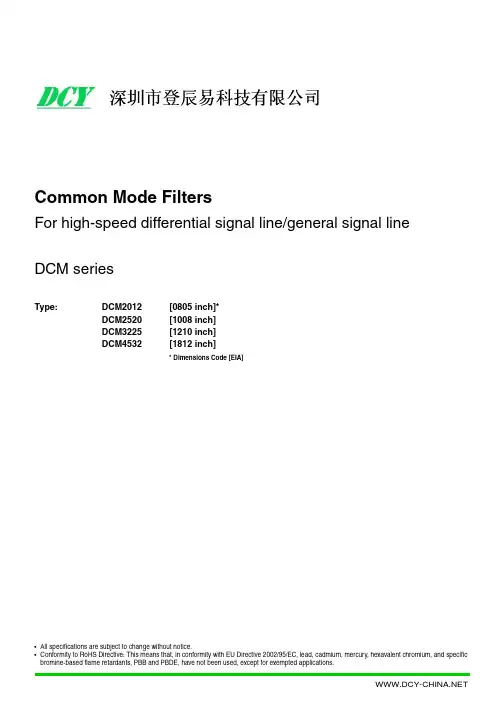
DCM4532[1812 inch]DCM3225[1210 inch]DCM2520[1008 inch]DCM2012[0805 inch]*DCM series•All specifications are subject to change without notice.•Conformity to RoHS Directive: This means that, in conformity with EU Directive 2002/95/EC, lead, cadmium, mercury, hexavalent chromium, and specific bromine-based flame retardants, PBB and PBDE, have not been used, except for exempted applications.Common Mode FiltersFor high-speed differential signal line/general signal line Type:* Dimensions Code [EIA](6) internal codeDCM4532DCM3225DCM2520DCM2012DCM Series DCM2012, 2520, 3225, 4532DCM 2012 -900-2P -T Common Mode FiltersFor High-speed Differential Signal Line / General Signal LineFEATURES•Although greatly miniaturized, this wire-wound chip-type filter maintains the characteristics needed for a common mode filter. Common mode impedance is 1000Ω [at 100MHz], so this filter is greatly effective in supporting noise.•Almost no affect upon even high speed signals since differential mode impedance is kept low.•This series includes both 2-line and 3-line types. They are used for various types of circuits and noise.APPLICATIONS•Used for radiation noise suppression for any electronic devices. •Used to counter common mode noise affecting signals within high-speed lines.•USB line for personal computers and peripheral equipment. •IEEE1394 line for personal computers, DVC, STB, etc.•LVDS, panel link line for liquid crystal display panels.TEMPERATURE RANGESPACKAGING STYLE AND QUANTITIESPRODUCT IDENTIFICATION (1) Series name(2) Dimensions L ×W 2012: 2.0×1.2mm(3) Impedance[at 100MHz]900: 90Ω(4) Number of line2P: 2-line 3P: 3-line(5) Packaging styleT: ø180mm reel taping TL: ø330mm reel taping RECOMMENDED SOLDERING CONDITIONS RECOMMENDED TEMPERATURE PROFILE FOR LEAD-FREE SOLDERREFLOW PROFILE FOR SOLDER HEAT RESISTANCEConformity to RoHS Directive Operating–25 to +85°C Storage(After mount)–25 to +85°CPackaging styleT ype Reel QuantityT apingø180mm 2000 pieces/reel ø330mm 10000 pieces/reel ø180mm 2000 pieces/reel ø330mm 10000 pieces/reel ø180mm 1000 pieces/reel ø330mm 5000 pieces/reel ø180mm 500 pieces/reel ø330mm2000 pieces/reel(1)(2)(3)(4)(5)(6)DCM2520-3P DCM4532-102-3PDCM2520-2P DCM3225-2PDCM2012-2PSHAPES AND DIMENSIONS/CIRCUIT DIAGRAMS/RECOMMENDED PC BOARD PATTERNS 2-LINE TYPE 3-LINE TYPEDCM4532-102-3P10000.6200.2DCM2520-801-3P 800 1.6200.15DCM3225-102-2P 10000.5200.2DCM3225-271-2P 2700.3200.3DCM3225-161-2P 1600.2200.35DCM3225-800-2P 800.15200.4DCM2520-102-2P 10000.9200.2DCM2520-601-2P 6000.45200.3DCM2520-451-2P 4500.4200.35DCM2520-301-2P 3000.35200.4DCM2012-361-2P 3600.5500.22DCM2012-201-2P 2000.25500.35DCM2012-121-2P 1200.22500.37DCM2012-900-2P 900.19500.4ELECTRICAL CHARACTERISTICSPart No.Impedance(Ω)typ.[100MHz]DC resistance(Ω)max.[per 1 line]Rated voltage Edc(V)max.Rated current Idc(A)max.2-LINE3-LINEDCM3225-271-2P DCM3225-102-2PDCM3225-800-2P DCM3225-161-2PDCM2520-601-2P DCM2520-102-2PDCM2520-301-2P DCM2520-451-2PDCM2012-201-2P DCM2012-361-2PDCM2012-900-2P DCM2012-121-2PMEASURING CIRCUITS 2-LINEDCM2520-801-3P DCM4532-102-3PIMPEDANCE vs. FREQUENCY CHARACTERISTICS 3-LINEMEASURING CIRCUITS 3-LINE。
DCM4532[1812 inch]DCM3225[1210 inch]DCM2520[1008 inch]DCM2012[0805 inch]*DCM series•All specifications are subject to change without notice.•Conformity to RoHS Directive: This means that, in conformity with EU Directive 2002/95/EC, lead, cadmium, mercury, hexavalent chromium, and specific bromine-based flame retardants, PBB and PBDE, have not been used, except for exempted applications.Common Mode FiltersFor high-speed differential signal line/general signal line Type:* Dimensions Code [EIA](6) internal codeDCM4532DCM3225DCM2520DCM2012DCM Series DCM2012, 2520, 3225, 4532DCM 2012 -900-2P -T Common Mode FiltersFor High-speed Differential Signal Line / General Signal LineFEATURES•Although greatly miniaturized, this wire-wound chip-type filter maintains the characteristics needed for a common mode filter. Common mode impedance is 1000Ω [at 100MHz], so this filter is greatly effective in supporting noise.•Almost no affect upon even high speed signals since differential mode impedance is kept low.•This series includes both 2-line and 3-line types. They are used for various types of circuits and noise.APPLICATIONS•Used for radiation noise suppression for any electronic devices. •Used to counter common mode noise affecting signals within high-speed lines.•USB line for personal computers and peripheral equipment. •IEEE1394 line for personal computers, DVC, STB, etc.•LVDS, panel link line for liquid crystal display panels.TEMPERATURE RANGESPACKAGING STYLE AND QUANTITIESPRODUCT IDENTIFICATION (1) Series name(2) Dimensions L ×W 2012: 2.0×1.2mm(3) Impedance[at 100MHz]900: 90Ω(4) Number of line2P: 2-line 3P: 3-line(5) Packaging styleT: ø180mm reel taping TL: ø330mm reel taping RECOMMENDED SOLDERING CONDITIONS RECOMMENDED TEMPERATURE PROFILE FOR LEAD-FREE SOLDERREFLOW PROFILE FOR SOLDER HEAT RESISTANCEConformity to RoHS Directive Operating–25 to +85°C Storage(After mount)–25 to +85°CPackaging styleT ype Reel QuantityT apingø180mm 2000 pieces/reel ø330mm 10000 pieces/reel ø180mm 2000 pieces/reel ø330mm 10000 pieces/reel ø180mm 1000 pieces/reel ø330mm 5000 pieces/reel ø180mm 500 pieces/reel ø330mm2000 pieces/reel(1)(2)(3)(4)(5)(6)DCM2520-3P DCM4532-102-3PDCM2520-2P DCM3225-2PDCM2012-2PSHAPES AND DIMENSIONS/CIRCUIT DIAGRAMS/RECOMMENDED PC BOARD PATTERNS 2-LINE TYPE 3-LINE TYPEDCM4532-102-3P10000.6200.2DCM2520-801-3P 800 1.6200.15DCM3225-102-2P 10000.5200.2DCM3225-271-2P 2700.3200.3DCM3225-161-2P 1600.2200.35DCM3225-800-2P 800.15200.4DCM2520-102-2P 10000.9200.2DCM2520-601-2P 6000.45200.3DCM2520-451-2P 4500.4200.35DCM2520-301-2P 3000.35200.4DCM2012-361-2P 3600.5500.22DCM2012-201-2P 2000.25500.35DCM2012-121-2P 1200.22500.37DCM2012-900-2P 900.19500.4ELECTRICAL CHARACTERISTICSPart No.Impedance(Ω)typ.[100MHz]DC resistance(Ω)max.[per 1 line]Rated voltage Edc(V)max.Rated current Idc(A)max.2-LINE3-LINEDCM3225-271-2P DCM3225-102-2PDCM3225-800-2P DCM3225-161-2PDCM2520-601-2P DCM2520-102-2PDCM2520-301-2P DCM2520-451-2PDCM2012-201-2P DCM2012-361-2PDCM2012-900-2P DCM2012-121-2PMEASURING CIRCUITS 2-LINEDCM2520-801-3P DCM4532-102-3PIMPEDANCE vs. FREQUENCY CHARACTERISTICS 3-LINEMEASURING CIRCUITS 3-LINE。
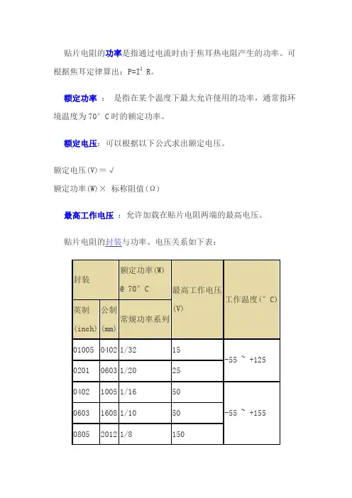
贴片电阻的功率是指通过电流时由于焦耳热电阻产生的功率。
可根据焦耳定律算出:P=I2 R。
额定功率:是指在某个温度下最大允许使用的功率,通常指环境温度为70°C时的额定功率。
额定电压:可以根据以下公式求出额定电压。
额定电压(V)=√额定功率(W)× 标称阻值(Ω)最高工作电压:允许加载在贴片电阻两端的最高电压。
贴片电阻的封装与功率、电压关系如下表:图1 (-55 ~+125)功率及环境温度降额曲线图图2 (-55 ~+155)功率及环境温度降额曲线图注意事项:•设计和使用贴片电阻时,最大功率不能超过其额定功率,否则会降低其可靠性。
•一般按额定功率的70%降额设计使用。
•也不能超过其最大工作电压,否则有击穿的危险。
•一般按最高工作电压的75%降额设计使用。
•当环境温度超过70°C,必须按照降额曲线图(图1,图2)降额使用。
我们俗称的封装是指英制。
规格书//电容规格书.pdf贴片电阻常见封装有9种,用两种尺寸代码来表示。
一种尺寸代码是由4位数字表示的EIA(美国电子工业协会)代码,前两位与后两位分别表示电阻的长与宽,以英寸为单位。
我们常说的0603封装就是指英制代码。
另一种是米制代码,也由4位数字表示,其单位为毫米。
下表列出贴片电阻封装英制和公制的关系及详细的尺寸:英制(inch ) 公制(mm)长(L)(mm)宽(W)(mm)高(t)(mm)a(mm)b(mm)02010603 0.60±0.050.30±0.050.23±0.050.10±0.050.15±0.0504021005 1.00±0.100.50±0.100.30±0.100.20±0.100.25±0.1006031608 1.60±0.150.80±0.150.40±0.100.30±0.200.30±0.2008052012 2.00±0.201.25±0.150.50±0.100.40±0.200.40±0.2012063216 3.20±0.201.60±0.150.55±0.100.50±0.200.50±0.201210 322 3.20±0. 2.50±0.0.55±0.0.50±0.0.50±0.Note:我们俗称的封装是指英制。


电感的封装种类电感封装发布时间:2009-12-02-9254封装在电子技术中一种专业术语。
指的形状及体积大小,重要部位用具体的数据来标示。
做PCB Layout时就要做一个元件封装的元件库,这个元件封装的尺寸将与元件本身的尺寸正公差一样,或比元件本身尺寸稍微大一点点。
做物料清单中如果把封装描述清楚,可以减少用错材料的机率。
电感的封装形式也就是指是电感的形状及体积大小的一种描述,电感封装根据每一个生产厂家不一家,描述方式也有不一样,一般包括贴片电感封装与插件电感封装。
插件电感封装有:PK0345、PK0406、PK0507、PK0608、PK0610、PK0810、PK0912、PK1012、PK1016、PK1415......;PK指的是工字电感系例,0406指的是不包括外被,直径是4mm 高度是6mm.贴片电感:0402、0603、0805、1206、CD32、CD43、CD52、CD53、CD54、CD73、CD75、CD104、CD105、CDR1608 CDR1813、CDR3308、CDR3316、CDR3340、CDR5022、2D11、2D18、3D16、3D28、4D18、4D28、5D18、5D28、6D28、6D38、8D28、8D38......0402、0603、0805、1206指的是叠层电感,CD32、CD43、CD52、CD53、CD54、CD73、CD75、CD104、CD105中CD指的是贴片的工字电感,32指的是直径3.5 高度2.3;43指的是直径4.5 高度为3.2贴片电感封装尺寸发布时间:2014-11-29-6668贴片电感封装尺寸SHAPES AND DIMENSIONS(形状及尺寸)(Unit:m/m)贴片电感封装尺寸列表绕线贴片电感封装发布时间:2010-10-17-2900绕线贴片电感封装SHAPES AND DIMENSIONS(形状及尺寸)(Unit:m/m)绕线贴片电感封装列表工字电感封装尺寸发布时间:2014-11-28-9062工字电感封装尺寸图SHAPES AND DIMENSIONS(形状及尺寸)(Unit:m/m)工字电感封装尺寸列表卧式工字电感尺寸发布时间:2010-10-17-2241卧式工字电感尺寸图SHAPES AND DIMENSIONS(形状及尺寸)(Unit:m/m)卧式工字电感尺寸列表色环电感封装尺寸发布时间:2010-10-17-3013色环电感封装尺寸SHAPES AND DIMENSIONS(形状及尺寸)(Unit:m/m)色环电感封装尺寸列表环形电感封装尺寸发布时间:2014-11-28-564环形电感封装尺寸:三脚电感封装尺寸发布时间:2014-11-28-2954三脚电感封装尺寸SHAPES AND DIMENSIONS(形状及尺寸)(Unit:m/m)东莞市欣永电子有限公司为你提供三脚电感封装尺寸及三脚电感封装尺寸图介绍等资料.功率电感封装发布时间:2010-12-25-4100功率电感封装SHAPES AND DIMENSIONS(形状及尺寸)(Unit:m/m)尺寸图表:贴片功率电感封装尺寸发布时间:2010-10-17-6730贴片功率电感封装尺寸SHAPES AND DIMENSIONS(形状及尺寸)(Unit:m/m)贴片功率电感封装尺寸列表大功率屏蔽电感封装发布时间:2010-10-17-3844大功率屏蔽电感封装SHAPES AND DIMENSIONS(形状及尺寸)(Unit:m/m)大功率屏蔽电感封装列表D系列屏蔽贴片电感封装尺寸发布时间:2014-09-08-4233屏蔽电感封装SHAPES AND DIMENSIONS(形状及尺寸)(Unit:m/m)2D11/2D14/2D18/3D11/3D14/3D16/3D284D14/4D18/4D22/4D28/5D18/5D28/6D26/6D388D28/8D38/8D43屏蔽电感封装列表UU系列共模电感封装尺寸发布时间:2014-11-19-724UU系列共模电感封装尺寸下载:•UU9.8共模电感封装尺pdf文档•UU10.5共模电感封装尺pdf文档•UU16共模电感封装尺pdf文档贴片排珠封装发布时间:2010-10-05-1613贴片排珠封装图:shapes and dimensions 形状与尺寸in:mm(供PCB layout参考)贴片排珠封装列表贴片磁珠封装发布时间:2010-10-05-3593贴片磁珠封装:1005(0402)、1608(0603)、2012(0805)、3216(1206)、3225(1806)、4532(1812)shapes and dimensions形状及尺寸in mm(供PCBlayout参考)贴片磁珠封装列表:穿芯磁珠尺寸发布时间:2010-10-18-2388穿芯磁珠尺寸图SHAPES AND DIMENSIONS(形状及尺寸)(Unit:m/m)穿芯磁珠尺寸列表。

C ustomer:·Technical Data Sheet PN:XGS-PB2012UB-02 For:IF=20mAContents1.Features2.Applications3.Package dimensions4.Absolute maximum rating5.Electrical optical characteristics6.BIN range7.Package label8.Soldering pad dimensions9.Soldering conditions10.Package tape specifications11.T ypical electro-optical characteristics curves12.Reliability test items and conditions13.Cautions14.Note◆F eatures:Compatible with automatic placement equipmentCompatible with reflow solder processLow power consumption and wide viewing angleThis product doesn’t contain restriction Substance, comply ROHS standard.◆A pplications:Automotive and TelecommunicationFlat backlight for LCD ,switch and symbol in telephone and faxGeneral use for indicators◆P ackage Dimensions:Unit:mmTolerenc e±0.1Electrodes: Ag Plating◆A bsolute Maximum Rating (Ta=25℃)* I FP condition: pulse width ≤1ms ,duty cycle ≤1/10◆E lectrical Optical Characteristics(Ta=25℃)Notes: 1.Tolerance of Luminous Intensity ±10%2.Tolerance of Dominant Wavelength ±2nm3.Tolerance of Forward Voltage ±0.05V4.Luminous Intensity is measured by XGSLED’s equipment on bare chips◆ Soldering Pad Dimensions:◆ S oldering Conditions (Maximum allowable soldering conditions)Reflow soldering profile<Pb-free solder>Time• Reflow soldering should not be done more than two times. • Do not stress its resin while soldering.• After soldering,do not warp the circuit board.T e m p e r a t u r e◆ P ackage Tape Specifications: (3000 pcs/Reel)Reel Lead Min.60mm No LEDs5 Reels in one Box10 Boxes in one Carton◆ T ypical Electro-Optical Characteristics Curves :Forward Current Vs Ambient Temperature5040302010100250Forward Current Vs Relative Luminosity204060801001020304050Ambient Temperature Ta (° C)Forward Current (mA)200 15010050 Relative Luminosity VsAmbient TemperatureIf=15mA-50° -60°-70°-80°-90°-40°-30°-20°-10°0°10°20°30°40°50°60°70°80°90° 0 0204060801001.00.50.5Radiation Angle1.0Ambient Temperature Ta (° C)R e l a t i v e L u m i n o s i t y (%)F o r w a r d C u r r e n t (m A )R e l a t i v e L u m i n o s i t y (%)◆Reliability(1)Test Items and Conditions(2)C riteria of judging the damage◆C autions1、PackageWhen moisture is absorbed into the package it may vaporize and expand during soldering. There is apossibility that this can cause exfoliation of the contacts and damage to the optical characteristics of the LEDs. So the moisture proof package is used to keep moisture to a minimum in the package.2、StorageBefore opening the package: The LEDs should be kept at 5~30°C and 60%RH or less. The LEDs should be used within a year.After opening the package: The LED must be used within 24 hours, else should be kept at 5~30℃and 30% RH or less. The LEDs should be used within 7days after opening the package. If unused LEDs remain, they should be stored in moisture proof packages, recommended to return the LEDs to the original moisture proof bag and to reseal the moisture proof bag again.If the LEDs have exceeded the storage time, baking treatment should be performed more than 24hours at 60±5°C.3、Soldering IronEach terminal is to the tip of soldering iron temperature less than 300℃ for 3 seconds within once inless than the soldering iron capacity 25 W.Leave two seconds and more internals, and do soldering of each terminal. Be careful because the damage of the product is often started at the time of the hand solder.4、RepairingRepairing should not be done after the LEDs have been soldered. When repairing is unavoidable, a double-head soldering iron should be used (as below figure). It should be confirmed beforehand whether the characteristics of the LEDs will or will not be damaged by repairing.5、The LED electrode sections are comprised of a gold plated. The gold surface may be affected by environments which contain corrosive gases and so on. Please avoid conditions which may cause the LED to corrode or discolor. This corrosion or discoloration may cause difficulty during soldering operations. It is recommended that the User use the LEDs as soon as possible.6、Please avoid rapid transitions in ambient temperature, especially in high humidity environments where condensation can occur.◆Notes:1、Above specification may be changed without notice. We will reserve authority on material change for above specification.2 、When using this product, please observe the absolute maximum ratings and the instructions for the specification sheets. We assume no responsibility for any damage resulting from use of the product which does not comply with the instructions included in the specification sheets.。

共模电感原理及在EMI中的应用[ 2009-3-18 10:52:00 | By: qqcandy ] 一、初识共模电感共模电感(Common mode Choke),也叫共模扼流圈,常用于电脑的开关电源中过滤共模的电磁干扰信号。
在板卡设计中,共模电感也是起EMI滤波的作用,用于抑制高速信号线产生的电磁波向外辐射发射。
图1:各种CMC小知识:EMI(Electro Magnetic Interference,电磁干扰)计算机内部的主板上混合了各种高频电路、数字电路和模拟电路,它们工作时会产生大量高频电磁波互相干扰,这就是EMI。
EMI还会通过主板布线或外接线缆向外发射,造成电磁辐射污染,不但影响其他的电子设备正常工作,还对人体有害。
PC板卡上的芯片在工作过程中既是一个电磁干扰对象,也是一个电磁干扰源。
总的来说,我们可以把这些电磁干扰分成两类:串模干扰(差模干扰)与共模干扰(接地干扰)。
以主板上的两条PCB走线(连接主板各元件的导线)为例,所谓串模干扰,指的是两条走线之间的干扰;而共模干扰则是两条走线和PCB地线之间的电位差引起的干扰。
串模干扰电流作用于两条信号线间,其传导方向与波形和信号电流一致;共模干扰电流作用在信号线路和地线之间,干扰电流在两条信号线上各流过二分之一且同向,并以地线为公共回路,如图1-1所示。
图1-1:串模干扰和共模干扰如果板卡产生的共模电流不经过衰减过滤(尤其是像USB和IEEE 1394接口这种高速接口走线上的共模电流),那么共模干扰电流就很容易通过接口数据线产生电磁辐射——在线缆中因共模电流而产生的共模辐射。
美国FCC、国际无线电干扰特别委员会的CISPR22以及我国的GB9254等标准规范等都对信息技术设备通信端口的共模传导干扰和辐射发射有相关的限制要求。
为了消除信号线上输入的干扰信号及感应的各种干扰,我们必须合理安排滤波电路来过滤共模和串模的干扰,共模电感就是滤波电路中的一个组成部分。