cyclone3的配置方式
- 格式:docx
- 大小:93.02 KB
- 文档页数:3
在对cyclone3配置时遇到的问题及配置的相关内容Cyclone III 器件的 AS 配置引脚与其他FPGA不同,其他FPGA 的 DA TA、DCLK、CSn、ASDO等引脚都是专用的,Cyclone III会使用另外的一些IO作为 EPCS 连接脚?有点晕!对cyclone3配置时,程序就是写不进去!目前来说问题出在一、核电压没有加上(vccint=1.2v)。
二、PLL的供电电压也没有加上(vcca=2.5v)。
三、配置引脚所用的BANK对应的电压也没有加上(vccio=3.3v)。
于是我注定写不进程序啊!!!DATASHEET中发现,这三个引脚一个不能少,这样子才能配置成功!另外的一些收获也记录一下吧。
一、有若干种配置模式,比如FAST AS,STANDARD AS等等,这个由MSEL【3:0】来设定。
二、VCCA is the analog power to the phase-locked loop (PLL).三、When using a JTAG configuration scheme or a serial configuration device in an AS configuration scheme, you must connect a 25ou series resistor at the near end of the TDO and TDI pin or the serial configuration device for the DATA[0]pin.四、After POR, the Cyclone III device family releases nSTATUS, pull-up resistor and enters which is pulled high by an external 10-k configuration mode.When nCONFIG goes high, the device exits reset and releases the open-drainnSTATUS pin, which pull-up resistor. After Ωis then pulled high by an external 10-k nSTATUS is released, the device is ready to receive configuration data and the configuration stage begins.五、ConfigurationConfiguration data is latched into the Cyclone III device family at each DCLK cycle.However, the width of the data bus and the configuration time taken for each schemeare different. After the device receives all the configuration data, the device releasesthe open-drain pull-up ΩCONF_DONE pin, which is pulled high by an external 10-kresistor. A low-to-high transition on the CONF_DONE pin indicates that configurationis complete and initialization of the device can begin. The CONF_DONE pin must havepull-up resistor for the device to initialize.Ωan external 10-kYou can begin reconfiguration by pulling the nCONFIG pin low. The nCONFIG pinmust be low for at least 500 ns. When nCONFIG is pulled low, theCyclone III devicefamily is reset. The Cyclone III device family also pulls nSTATUS and CONF_DONE lowand all I/O pins are tri-stated. When nCONFIG returns to a logic-high level andnSTATUS is released by the Cyclone III device family, reconfiguration begins.六、User ModeAn optional INIT_DONE pin is available that signals the end of initialization and thestart of user mode with a low-to-high transition. The Enable INIT_DONE Outputoption is available in the Quartus II software from the General tab of the Device andPin Options dialog box. If you use the INIT_DONE pin, it is high due to an external10-k pull-up resistor when nCONFIG is low and during the beginning ofconfiguration. After the option bit to enable INIT_DONE is programmed into thedevice (during the first frame of configuration data), the INIT_DONE pin goes low.When initialization is complete, the INIT_DONE pin is released and pulled high. Thislow-to-high transition signals that the device has entered user mode. In user mode,the user I/O pins function as assigned in your design and no longer have weakpull-up resistors.七、整个过程应该是program>>configuration>>initialiaition.进入user mode。

ETL-002 Altera Cyclone III系列FPGA开发板简介概述ETL-002 FPGA开发板是以Altera公司的最新系列Cyclone III中的3C10为主芯片,并提供了极为丰富的芯片外围接口资源以及下载线,数据线以及资料光盘等。
除了这些硬件外,我们还提供了十多个接口实验,并公开了电路原理图和实验的Verilog源代码,以便于大家对照学习,并可以在该开发板上进行二次开发。
单板描述主芯片EP3C10提供了10320个逻辑单元(LE),46块SRAM(每块9K bits), 23个18*18的乘法器。
开发板自带USB供电电路:您只需将USB线插上您的USB端口,无需外接+5V直流电源,开发板即可工作。
开发板同时支持AS模式下载和JTAG模式下载。
程序固化既可通过JTAG口也可直接对板上的FLASH进行编程。
丰富的外围接口可满足常用的外设的人机交互,我们还将剩下未用的40个用户I/O引脚全部引出,使得您可以通过这些信号对本开发板进行电路扩展。
这些接口主要包括:PS2鼠标接口:可以将PS2鼠标的任何移动的信息反应在数码管上PS2键盘接口:可以将PS2键盘上的任意按键以16进制的信息反应在数码管上VGA显示器接口:可以将FPGA产生的信息反映在VGA显示器上。
开发板自带了动态彩条显示的功能双串口接口:可以与任何的串口设备相接。
开发板自带的演示程序是将PC上的超级终端中输入的任何信息返回PC 4位数码管:可以实时显示任何的数字信息。
开发板自带的演示程序实时地显示分钟和秒钟的信息。
4位LED灯:用于指示状态。
开发板自带了跑马灯实验。
4位按键开关:可用于复位等作用。
4位拨码开关:可用于电路的选择作用教学实验除了开发板的丰富的硬件资源外,我们还提供了数十个学习实验。
通过这些实验,您可以学习FPGA芯片,Quartus II软件和设计仿真和下载等FPGA的设计流程,然后将试验中程序执行的信息通过数码管,LED 灯,串口等板上的硬件直观的显示出来。
Cyclone III原型开发调试转载:/ilove314/1819329/Message.aspx 最近设计的Cyclone III原型板是特权同学第一次接触Cyclone III的器件。
原理图、PCB绘制、管脚分配上都碰到了一些问题,这些问题或多或少都是由于个人对新器件不熟悉、设计的时候有一些粗心大意造成的。
主要针对板级的硬件设计,这里凌乱的罗列一下,做一点总结,今后要多吸取教训,低级的失误要尽量避免。
1. 首先要提一个没有解决的问题,EP3C5E144/EP3C10E144/ EP3C16E144/ EP3C 25E144(是管脚完全兼容的不同资源的器件,Altera在这一点上是非常值得称道的)器件的PIIN11和PIN12存在不可同时使用的问题,这个问题出现在架构了一个NIOS2系统里集成了EPCS控制器的时候,在Cyclone II中是不需要分配这个EPCS控制器的管脚的(内部自动映射),而Cyclone III则需要手动分配(事先需要到Setting里动动手脚)。
EPCS的DCLK需要分配到PIN12上,工程中分配了一个SDRAM的D0脚给PIN11,编译到Fitting阶段就Error了。
在handbook里海找没什么成效,求助于搜索引擎,最终看到有人遇到相同的问题,但是给出的却是不是办法的解决办法:不用PIN11或者不用PI N12。
这个问题上特权同学也很是无可奈何,估计是Cyclone III器件的这两个脚做了一些信号耦合之类的检查,也不知道是否在工具选项里做一些设置可以取消此类检查。
也很期待有相同遭遇的朋友现身说法,告诉特权如何解决问题。
2. 再说两个很低级的错误,错的很傻,没有什么技术含量,只能给自己敲个警钟:干活的时候脑子一定要清醒。
两个错误分别和BOM表和网络标号有关。
先说和BOM表有关的,这个错误源于原理图上两个三端稳压器-1.2和-2.5的标示刚好反过来了,因为管脚定义和封装都一样所以也没留意,好在最后只影响BOM表的标示,但这也导致了第一块样板焊接的时候出现了1.2V和2.5V互换位置的惨剧,结果可想而知,EP3C10E144C7就这样挂了,非常的心疼。

将两层板进行到底,搞起CycloneIII我以前DIY过两个FPGA的板子,都是Altera Cyclone II的。
几年前就买了的几片Cyclone III EP3C10一直没动,除了还没有DIY 项目必须要用到它外,还有个原因是Cyclone III系列需要3组电压供给,在两层板上走线不太好弄。
我也看到过别人在用两层PCB做的Cyclone III的设计,能跑起来说明也不是不可行。
今年已经DIY过两个带SDRAM的MCU板子,都是两层PCB。
这次我继续挑战一下,在两层板上把EP3C10加SDRAM搞起来,打算玩一玩NIOS II. 经过长时间的Layout斟酌,上个月总算把这个PCB 做出来了。
和我的前两个FPGA实验板不同的是,我这次设计成了核心板的形式,只保留FPGA+SDRAM以及必要的外围元件,把扩展GPIO接口和应用相关的接口件都挪到扩展板上去。
核心板和扩展板使用2.0 pitch的双排针/座来连接。
做出来是这个效果(简单做了几个2.54排针,以及JTAG座扩展卡):比如只需要用USB Blaster进行JTAG下载的时候,是这样用的(示意一下,另外还需要连3.3V电源)板子的背面:有2.5V和1.2V的LDO, 都是小封装的。
SDRAM还没有焊,待我把NIOS玩起来了再焊它调试。
扩展的排插是2.0 pitch,一方面是减小体积,另一方面是这种双排母比常见2.54的排母接触好。
正面:晶振也用3225的,比7050的省地方。
我手头恰好没有3225了,就焊了个2520更小尺寸的。
右边白色的插座是1.25 pitch 的连接器,可接6pin排线,用于少量I/O的扩展,连其它板子。
原理图:还是用我DIY一贯的EagleCyclone III 需要至少3组电压:1.2V的VCCINT, 2.5V的VCCA,以及平常3.0/3.3V的VCCIO. SDRAM只用到3.3V.Layout费了番心思。
101 Innovation DriveSan Jose, CA 95134Cyclone III FPGA Starter KitUser GuideDocument Version: 1.2Document Date: July 2010P25-36228-03© 2010 Altera Corporation. All rights reserved. ALTERA, ARRIA, CYCLONE, HARDCOPY, MAX, MEGACORE, NIOS, QUARTUS and STRATIX are Reg. U.S. Pat. & Tm. Off. and/or trademarks of Altera Corporation in the U.S. and other countries. All other trademarks and service marks are the property of their respective holders as described at /common/legal.html. Altera warrants performance of its semiconductor products to current specifications in accordance with Altera's standard warranty, but reserves the right to make changes to any products and services at any time without notice. Altera assumes no responsibility or liability arising out of the application or use of any information, product, or service described herein except as expressly agreed to in writing by Altera. Altera customers are advised to obtain the latest version of devicespecifications before relying on any published information and before placing orders for products or services.Part Number UG-01018-1.2ContentsChapter 1. Getting StartedIntroduction............................................................................................................................................1–1 Before You Begin...................................................................................................................................1–2 Further Information..............................................................................................................................1–2 Software Installation.............................................................................................................................1–2 Installing the Cyclone III FPGA Starter Kit..................................................................................1–2 Installing the Quartus II Web Edition Software..........................................................................1–4 Chapter 2. Development Board and Control Panel SetupDevelopment Board Setup...................................................................................................................2–1 Requirements....................................................................................................................................2–2 Powering Up the Development Board..........................................................................................2–2 Installing the USB-Blaster Driver........................................................................................................2–2 Control Panel Setup...............................................................................................................................2–3 Configuring the FPGA Using the Quartus II Programmer.............................................................2–3 Chapter 3. Using the Control PanelOverview.................................................................................................................................................3–1 Control Panel Start................................................................................................................................3–1 LEDs and Buttons..................................................................................................................................3–2 Illuminating LEDs............................................................................................................................3–2 Buttons Indicators............................................................................................................................3–3 DDR SDRAM/SSRAM/On-Chip Controller...............................................................................................................3–3 Read/Write Data..............................................................................................................................3–4 Read from a File................................................................................................................................3–5 Write to a File...................................................................................................................................3–5 Flash Memory Programmer.................................................................................................................3–5 Flash Memory Tab...........................................................................................................................3–6 CFI Query..........................................................................................................................................3–6 Read/Write Data..............................................................................................................................3–7ContentsChapter 4. Measuring Power on the Cyclone III Starter BoardIntroduction............................................................................................................................................4–1 Measuring Power...................................................................................................................................4–2 Changing the Example Design.......................................................................................................4–3 Appendix A. Programming the Configuration Flash DeviceOverview................................................................................................................................................A–1 Creating a Flash-Programmable POF File........................................................................................A–1 Programming the Flash Device..........................................................................................................A–5 Additional InformationRevision –i How to Contact –ii Typographic –ii1.Getting StartedIntroduction Welcome to the Altera® Cyclone®III FPGA Starter Kit, which includes afull-featured field-programmable gate array (FPGA) development board,hardware and software development tools, documentation, andaccessories needed to begin FPGA development.The development board includes an Altera Cyclone III FPGA and comespreconfigured with a hardware reference design stored in flash memory.You can use the development board as a platform to prototype a varietyof FPGA designs.The starter kit provides an integrated control environment that includesa software controller in a control panel application, a USB commandcontroller, a multi-port SRAM/DDR SDRAM/flash memory controller,and example designs specified in Verilog code. You can use this design asa starting point for test designs.This user guide addresses the following topics:■How to set up, power up, and verify correct operation of thedevelopment board.■How to install the Cyclone III FPGA Starter Kit.■How to install the Altera® Quartus II Web Edition software.■How to set up and use the control panel, a graphical user interface(GUI), to manipulate components on the board, implementapplications.■How to configure the Cyclone III FPGA.■How to set up and run example designs.f For complete details on the development board, refer to theCyclone III FPGA Starter Board Reference Manual.Before You BeginBefore You Begin Before proceeding, check the contents of the kit:■Cyclone III FPGA Starter Development Board ■12-V DC power supply■USB cablef For the most up-to-date information on this product, visit the Alterawebsite at /products/devkits/altera/kit-cyc3-starter.html.FurtherInformationFor other related information, refer to the following websites:Software Installation This section describes the following procedures:■“Installing the Cyclone III FPGA Starter Kit”■“Installing the Quartus II Web Edition Software” on page1–4 Installing the Cyclone III FPGA Starter KitThe license-free Cyclone III FPGA Starter Kit installer includes all the documentation and design examples for the kit.To install the Cyclone III FPGA Starter Kit, follow these steps:1.Download the Cyclone III FPGA Starter Kit installer from theCyclone III FPGA Starter Kit page of the Altera website.Alternatively, you can request a development kit DVD from theDevelopment Kits, Daughter Cards & Programming Hardware page of the Altera website.For More Information About Refer ToAdditional daughter cardsavailable for purchase/products/devkits/kit-daughter_boards.jspCyclone III handbook /literature/lit-cyc3.jspCyclone III reference designs /products/devkits/altera/kit-cyc3-starter.htmleStore if you want topurchase devices/buy/devices/buy-devices.htmlCyclone III Orcad symbols /support/software/download/pcb/pcbpcb_index.htmlNios® II 32-bit embeddedprocessor solutions/technology/embedded/emb-index.htmlGetting Started 2.Follow the on-screen instructions to complete the installationprocess.The installation program creates the Cyclone III FPGA Starter Kit directory structure shown in Figure1–1.Figure1–1.Cyclone III FPGA Starter Kit Default Installed Directory StructureTable1–1 lists the file directory names and a description of their contents.Table1–1.Installed Directory ContentsDirectory Name Description of Contentsboard_design_files Contains schematic, layout, assembly, and bill of materialboard design files. Use these files as a starting point for anew prototype board design.demos Contains demonstration projects that may or may notcontain up-to-date source code.documents Contains the development kit documentation.examples Contains the example design files for the Cyclone III FPGAStarter Kitfactory_recovery Contains programming files for returning board to factorydefault condition.Software InstallationInstalling the Quartus II Web Edition SoftwareThe Quartus II Web Edition software provides the necessary tools fordeveloping hardware and software for Altera FPGAs. Included in theQuartus II Web Edition software are the Quartus II software, the Nios IIEDS, and the MegaCore® IP Library. The Quartus II software (includingSOPC Builder) and the Nios II EDS are the primary FPGA developmenttools for creating the reference designs in this kit.To install the Quartus II Web Edition software, follow these steps:1.Download the Quartus II Web Edition software from the Quartus IIWeb Edition Software page of the Altera website. Alternatively, youcan request a DVD from the Altera IP and Software DVD RequestForm page of the Altera website.2.Follow the on-screen instructions to complete the installationprocess.f If you have difficulty installing the Quartus II software,refer to Quartus II Installation & Licensing for Windows andLinux Workstations.The Quartus II Web Edition software includes the following items:■Quartus II software—The Quartus II software, including the SOPCBuilder system development tool, provides a comprehensiveenvironment for system-on-a-programmable-chip (SOPC) design.The Quartus II software integrates into nearly any designenvironment and provides interfaces to industry-standard EDAtools.f To compare the Quartus II subscription and web editions,refer to Altera Quartus II Software—Subscription Edition vs.Web Edition. The kit also works with the subscriptionedition.■MegaCore IP Library—A library that contains Altera IP MegaCorefunctions. You can evaluate MegaCore functions with the OpenCorePlus feature to perform the following tasks:●Simulate behavior of a MegaCore function in your system●Verify functionality of your design, and quickly and easilyevaluate its size and speed●Generate time-limited device programming files for designs thatinclude MegaCore functions●Program a device and verify your design in hardwareGetting Started 1The OpenCore Plus hardware evaluation feature is anevaluation tool for prototyping only. You must purchase alicense to use a MegaCore function in production.f For more information about OpenCore Plus, refer toAN320: OpenCore Plus Evaluation of Megafunctions.■Nios® II Embedded Design Suite (EDS)—A full-featured tool set that allows you to develop embedded software for the Nios II processor which you can include in your Altera FPGA designs.Licensing ConsiderationsThe Quartus II Web Edition software is license-free and supports Cyclone III devices without any additional licensing requirement. This kit also works with the Quartus II Subscription Edition software, after you obtain the proper license file. To purchase a subscription, contact your Altera sales representative.Software Installation2.Development Board andControl Panel Setup DevelopmentBoard SetupThe development board is preloaded with an example design todemonstrate the Cyclone®III device and board features. At power-up,the preloaded design also enables you to quickly confirm that the boardis operating correctly.Figure2–1 shows the Cyclone III development board layout andcomponents.Figure2–1.Cyclone III Development Board Layout and Components1-Mbyte SSRAM (U5)DC PowerInput (J2)Power Switch (SW1)16-MbyteParallelFlash (U6)ConnectorFlash LEDUSBUART (U8)JT AG Header (J4)32-MbyteDDR SDRAM (U4)Reconfigureand ResetPush Buttons50-MHzSystem ClockUser LEDsUser Push Button SwitchesHSMCConnector (J1)Cyclone III Device (U1)Configuration Done LEDSense Resistor for FPGACore Power Measurement (JP6)Sense Resistorfor Shared I/OAltera Corporation 2–1Installing the USB-Blaster DriverRequirementsBefore you proceed, ensure that the follwing items are installed:■Altera® Quartus®II software on the host computer■Cyclone III FPGA Starter Kit■USB-Blaster™ driver software on the host computer. TheCyclone III FPGA starter development board includes an integratedUSB-Blaster circuitry for FPGA programming.Powering Up the Development BoardTo power-up the development board, follow these steps:1.Ensure that the ON/OFF switch (SW1) is in the OFF position (up).2.Connect the USB-Blaster cable from the host computer to theUSB-Blaster port on the development board.3.Connect the 12-V DC adapter to the development board and to apower source.w Only use the supplied 12-V power supply. Power regulationcircuitry on the board could be damaged by supplies greaterthan 12V.4.Press the power switch (SW1).5.Confirm that all four user LEDs are ON.Installing the USB-Blaster Driver The Cyclone III FPGA development board includes an integratedUSB-Blaster circuitry for FPGA programming. However, for the host computer and board to communicate, you must install the USB-Blaster driver on the host computer.Installation instructions for the USB-Blaster driver are available on the Altera website at /support/software/drivers/dri-index.html. On the “Altera Programming Cable Driver Information” page of the Altera website, locate the table entry for your configuration and click the link to access the instructions.2–2Altera CorporationDevelopment Board and Control Panel SetupControl Panel Setup Setting up the control panel involves the following:■Configuring the FPGA■Starting the control panel1Power up the board and ensure that is is operational.For more information about using the control panel, refer to the “Using the Control Panel” chapter.Configuring the FPGA Using the Quartus II Programmer You can use the Quartus II Programmer to configure the FPGA with a specific .sof. Before configuring the FPGA, ensure that the Quartus II Programmer and the USB-Blaster driver are installed on the host computer, the USB cable is connected to the development board, power to the board is on, and no other applications that use the JTAG chain are running.To configure the Cyclone III FPGA, follow these steps:1.Start the Quartus II Programmer.2.Click Add File and select the path to the desired .sof.3.Turn on the Program/Configure option for the added file.4.Click Start to configure the selected file to the FPGA. Configurationis complete when the progress bar reaches 100%.Altera Corporation 2–3Configuring the FPGA Using the Quartus II Programmer2–4Altera Corporationing the Control PanelOverview The control panel consists of the following:■The graphical user interface (GUI) application on the host computer■The standard Nios II hardware design running on the board'sCyclone III FPGA deviceAfter installing the Cyclone III FPGA Starter Kit, you can locate thecontrol panel for the hardware and software in the<kit path>\demos\control_panel directory.The design downloaded to the Cyclone III device implements acommand controller that processes board commands sent over theUSB-Blaster from the control panel. To perform the appropriate actions,the command controller communicates with the controller of the targetedboard I/O device.You can perform the following actions with the control panel:■Light up LEDs■Detect push button presses■Read from and write to the DDR SDRAM, SRAM, flash memory, andon-chip RAMThe following sections describe how to perform the above actions withthe control panel already open on the host computer. If not already open,launch the control panel as described in “Control Panel Start”.Control Panel Start The Cyclone III development board is shipped with an example design stored in the flash memory which configures the Cyclone III FPGA upon power-up with the standard Nios II design.1For an older version of the Cyclone III development board shipped with the Cyclone III FPGA Starter Kit v7.1.0, v7.2.0, or8.0.0 application, you must manually configure thecycloneIII_3c25_start_niosII_standard.sof into the FPGAbefore launching the control panel application.Altera Corporation 3–13–2Altera Corporation LEDs and ButtonsYou can locate the source for the example design in the <kitpath>\examples\cycloneIII_3c25_starter_board_standard directory. 1To launch the control panel user interface, run thecontrol_panel.exe program found in the <kitpath >\demos\control_panel directory (Figure 3–1).Figure 3–1.Control Panel WindowLEDs andButtons Illuminating LEDs To illuminate an LED, follow these steps:1.The LED & Buttons tab should be visible when the application runs.If it is not visible, click the LED & Buttons tab (Figure 3–2).2.Click on LEDs to individually turn on the LEDs.Using the Control PanelButtons Indicators1.Press the push-button switches on the board. Notice that buttons onthe GUI change accordingly.Figure3–2.Control Panel Window for LEDs and ButtonsDDR SDRAM/ SSRAM/On-Chip Controller You can perform the following types of memory read/write operations with the control panel:■Read from and write to the DDR SDRAM, SSRAM, or on-chip device ■Write entire contents of a file, to the DDR SDRAM, SSRAM, or on-chip device■Read contents of the DDR SDRAM, SSRAM, or on-chip device, to afileAltera Corporation 3–33–4Altera Corporation DDR SDRAM/ SSRAM/On-Chip ControllerThe following sections describe how to access the DDR SDRAM. You can use the same procedure to access the SSRAM.Read/Write DataTo read from and write to the DDR SDRAM, follow these steps:1.Click the DDR SDRAM tab (Figure 3–3). The Address columnindicates the hex address of the DDR SDRAM. The values inside the 0-3, 4-7, 8-B , and C-F columns are the DDR SDRAM contents in hex words format.Figure 3–3.Control Panel DDR SDRAM Tab2.To write a 32-bit word to the DDR SDRAM, click the desiredlocation, enter the desired value in hex format, and press Enter.Using the Control PanelRead from a FileTo read the contents of a file and load it to the DDR SDRAM, follow these steps:1.Click Load File.2.Browse to sample.txt located in the control_panel directory andclick Open. This step instantiates the DDR SDRAM controller and loads the text contents into the DDR SDRAM. Notice that the Data to Ascii-text column shows the DDR SDRAM contents in Asciivalue.Write to a FileTo write the contents of the DDR SDRAM to a file, follow these steps:1.Click Save File.2.Enter the start and end addresses of the DDR SDRAM.3.Choose a file name and click Save. This instantiates the controller toread the DDR SDRAM contents from the start address to the endaddress, and write the contents to a file.Flash Memory Programmer You can perform the following operations to read from and write to the board’s flash memory with the control panel:■Perform a CFI query of flash memory■Erase select blocks of flash memory■Write 32-bit hex word to flash memory■Write a binary file to flash memory■Load the contents of the flash memory into a filec Do not exit from the control panel while erasing the flashmemory.Altera Corporation 3–5Flash Memory ProgrammerFlash Memory TabTo use the flash memory functions, click the Flash Memory tab(Figure3–4).Figure3–4.Control Panel Flash Memory TabCFI QueryThe common flash interface (CFI) flash memory devices conform to basicflash commands. The most basic command is Query which switches thedevice into a ROM table mode so that features of the flash device aredetermined by reading values from the table.To perform a CFI query using the host application, click CFI Query.Notice that the memory table displays contents that correlate with thetable contents as described in the device datasheet.To put the flash device back in user mode, press Reset on the controlpanel.3–6Altera CorporationAltera Corporation 3–7Using the Control PanelRead/Write DataTo read from and write to the flash memory, follow these steps:Figure 3–5.Control Panel Flash Memory Tab1.Click Erase Block to perform a block erase of the flash memory. The Address column indicates the hex address of the flash memory. The values inside the 0-3, 4-7, 8-B , and C-F columns are the flash memory contents in hex words format.2.To write a 32-bit word to the flash memory, click the desired location, enter the desired value in hex format, and press Enter.Flash Memory Programmer3–8Altera Corporation4.Measuring Power on theCyclone III Starter BoardIntroduction One of the main features of the Cyclone®III device is its low powerconsumption. You can measure the power of the 3C25 device on theCyclone III starter board under various conditions with an exampledesign provided with the kit.The power example design allows you to control the amount of logicutilized in the FPGA, the clock frequency, the number of I/Os being used,and measure the effect on the power to the Cyclone III device. Because theCyclone III starter board has only four buttons and four LEDs, interactionwith the board is minimal as defined below.Table4–1 describes the functionality of the four input buttons that controlthe power example design.Tables4–2 and 4–3 describe how the LEDs indicate the example design’scurrent power state.Table4–1.Four Input Button FunctionalityButton FPGA Pin Type Description1F1Reset Resets the demo to the beginning, nodei_nrst.2F2Toggle Advances the example design to the next higherfrequency, node i_nfreq_next.3A10Toggle Advances the example design to the next higherresource utilization, node_i_nperc_next.4B10Press and Hold Enables the outputs to toggle, nodei_noutput_ena.Table4–2.LEDs Power State (Frequency)DisplaysLEDsStateClock Frequency(MHz)MSB LSBFrequency LED2 LED10000133106711100Altera Corporation 4–14–2Altera CorporationMeasuring PowerThe design used for power measurement is a replicated set of randomly filled ROMs that feed a multiplier block and a shift register that is fed by a signal that changes every clock cycle. Tables 4–2 and 4–3 show the power state which represent the percent of the full design used. As compiled, this full design uses:■Logic elements: 22,493/24,624 (91%)■Combinational functions: 1,961/24,624 (8%) ■Dedicated logic registers: 21,133/24,624 (86%) ■Total registers: 21,133 ■Total pins: 73/216 (34%)■Total memory bits: 524,288/608,256 (86%)■Embedded Multiplier 9-bit elements: 128/132 (97 %)■Total PLLs: 1/4 (25%)Measuring PowerThe example design is located in<kit install >\examples\cycloneIII_3c25_start_power_demo . Configure the FPGA with the .sof found in the directory. 1The input clock (i_clk PIN_B9) is the 50-MHz oscillator on the board, which generates the input clock for the reference design through a PLLfFor more information on configuring the FPGA, refer to “Configuring the FPGA Using the Quartus II Programmer” on page 2–3.Current sense resistors (0.010 ± 1%) are installed at locations JP6 (FPGA core power) and JP3 (FPGA I/O power + other device I/O power). With a digital multimeter set to mV measurement range, the resistor at location JP6 measures the core power. The resistor at location JP3 measures the I/O power. To measure the current being used in various configurations, use the following steps:Table 4–3.LEDs Power State (Resources)DisplaysLEDsState% of Design UsedMSBLSBResourcesLED4LED30025%0150%1075%11100%Measuring Power on the Cyclone III Starter Board1To obtain the power (P) in milliwatts, measure <MeasuredVoltage> (the voltage across the sense resistors at JP6 or JP3) inmV and calculate the nominal power using the equation:P = 100 x <Measured Voltage> x <Supply Voltage>where <Supply Voltage> is 1.2 V for JP6 and 2.5 V for JP3.You can use the four input buttons to advance through the various powerstate as outlined in Table4–2. Notice how current increases as frequencyand resource usage increase.You can also measure the I/O power consumed by measuring the voltageacross sense-resistor JP3 when Button 4 is pressed and held. Because this2.5-V power rail is shared with other devices, there is a nominal 100mWthat must be subtracted from the calculated I/O power to obtain theFPGA I/O power.The number of I/O pins used is controlled by the resource state (shownin Tables4–2 and 4–3). For each increment in resources, 16 additional I/Opins are added (refer to Table4–4).Table4–4.I/O Pin & Resource StateLED4/LED3Number of I/O Pins0016013210481164Similarly, the toggle-frequency of these I/O pins is set by the overalldesign frequency (refer to Table4–1).Changing the Example DesignThe source code for the Cyclone III power example design is alsoprovided so you can use it as a starting point for your own measurements.You can adjust the number of outputs by changing parameterNUM_OUTPUTS_PER_STAMP. The default is 16, which for four resourcepercentage steps equates to 16 x 4 = 64.The appropriate pins to be used as outputs are pre-assigned to the HSMCconnector (J1). If you would like to look at more than the 76 I/Os availableon J1, you need to make the appropriate pin assignments.Altera Corporation 4–3。
摘要:本文主要通过介绍Cyclone 系列FPGA 器件的配置方案,主要阐述了低成本专用配置芯片的主动串行(AS )配置方案以及基于微处理器的被动串行(PS )配置方案的配置过程。
介绍了如何结合工程设计选择配置方案,改变现在的任意选择配置方案的现象。
提出一种实时解压数据减少贮存要求和配置时间的配置方案,这些方案在工程项目中具有很高的实际应用价值。
关键词:Cyclone FPGA 配置模式主动串行被动串行0引言FPGA 是英文Field -Programmable Gate Array 的缩写,即现场可编程门阵列,它是在PAL 、GAL 、CPLD 等可编程器件的基础上进一步发展的产物。
FPGA 技术广泛应用于通讯、视频、信息处理等特定领域。
FPGA 主要生产厂商有Altera 、Xilinx 、Actel 和Lattice ,对比不同的FPGA 编程技术特点,综合各个厂家不同系列器件的技术优势、逻辑资源、器件功耗、芯片速度、供货、价格和系统要求等诸多因素考虑,在很多项目设计中采用Altera 公司基于SRAM 架构Cyclone 系列器件。
Cyclone 器件与其他FPGA 器件一样是基于门阵列方式为用户提供可编程资源的,其内部逻辑结构的形成是由配置数据决定的。
这些配置数据可通过多种模式加载到FPGA 内部的SRAM 中,由于SRAM 的易失性,每次上电时,都必须对FPGA 进行重新配置。
1Cyclone FPGA 配置模式Cyclone 系列FPGA 器件配置方案主要有三种,包括使用低成本配置芯片的主动串行(AS )配置、被动串行(PS )配置以及基于JTAG 配置,实际应用时可以使用其中的一种方案配置Cyclone 系列FPGA 器件,来实现用户编程所要实现的功能。
Cyclone 系列FPGA 器件是用SRAM 单元配置数据的。
由于SRAM 掉电后容易丢失数据,配置数据必须即时地下载到上电的Cyclone 器件中。
Cyclone III中LVDS的设计一,概述LVDS低压差分信号,最早由美国国家半导体公司提出的一种高速串行信号传输电平,由于它传输速度快,功耗低,抗干扰能力强,传输距离远,易于匹配等优点,迅速得到诸多芯片制造厂商和应用商的青睐,并通过TIA/EIA的确认,成为该组织的标准(ANSI/TIA/EIA-644 standard)。
LVDS信号被广泛应用于计算机、通信以及消费电子领域,并被以PCI-Express为代表的第三代I/O标准中采用。
LVDS信号的电压摆幅只有350MV,为电流驱动的差分信号方式工作,最长的传输距离可以达到10米以上。
为了确保信号在传输线当中传播时,不受反射信号的影响,LVDS信号要求传输线阻抗受控,其中单线阻抗为50ohms,差分阻抗100ohms。
在实际应用当中,利用一些高速电路仿真分析工具,通过合理的设置层叠厚度和介质参数,调整走线的线宽和线间距,计算出单线和差分阻抗结果,来达到阻抗控制的目的。
LVDS的工作原理是其中发送端是一个为3.5mA的电流源,产生的3.5mA的电流通过差分线的其中一路到接收端。
由于接收端对于直流表现为高阻,电流通过接收端的100欧姆的匹配电阻产生350mV的电压,同时电流经过差分线的另一条流回发送端。
当发送端进行状态变化时它通过改变流经100欧姆电阻的电流的方向产生有效的'0'和'1'态。
二,硬件设计为了达到阻抗控制的要求,PCB的设计采用常见的4层板,基本叠层结构如下图:板子的总体厚度约为1.6mm,L1,L4为信号层,L2,L3分别为地线层和电源层,半固化片采用2116,根据CTS的计算,选取差分线线宽6mil,间距8mil,信号层铺铜厚度为0.5OZ(完成后约为高度48um),可以达到差分阻抗约100欧姆。
在CIII芯片中,有多组可以输出LVDS信号的IO,但有几点需要注意。
在芯片的right bank,left bank上,也就是1,2,5,6 bank,设计了“dedicated output buffer”,这些IO不要添加其他器件既可以输出LVDS信号,也就是说不需要做任何电阻网络匹配的工作了。
Cyclone_III配置Cyclone III 的配置全文翻译自Altera公司Cyclone III的器件手册。
所有表格与图标标号与手册原文一致,以便于查对。
出于个人需要,仅翻译了AS与JTAG配置两部分,且仅都配置一片FPGA芯片。
可以通过压缩数据的方法以节约存储空间,并节省程序load时间(page 220);9通过Remote System Upgrade方式可以减少新产品面市的时间(page 221);9AS Configuration(Serial Configuration Devices)表10-6显示的是对各种配置电平来说,MSELx管脚的接法单一器件配置四个接口管脚包含了串口时钟(DCLK),串行数据输出(DATA),AS 数据输入(ASDI),以及低电平有效的片选信号(nCS)。
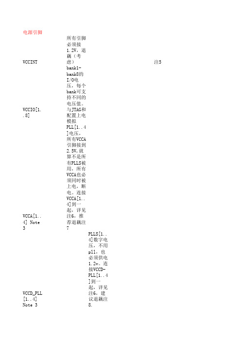
注:1)上拉一个电阻,连接到该管脚所在的bank的VCCIO;2)Cyclone III器件通过DATA[1]-to-ASDI路径控制配置芯片;3)nCEO管脚浮空,或者当没有连接到另一个器件的nCE管脚时,可以当作通用IO使用;4)MSEL管脚的设置,用于选择不同的电平标准和不同的POR时间;参考表10-6,选择接法;5)这些是复用管脚。
FLASH_nCE管脚在AS配置电路图中当作nCSO功能使用,DATA[1]管脚当作ASDO功能使用;6)这些串接的电阻尽可能靠近配置芯片当连接一个配置芯片到Cyclone III器件时,DATA[0]管脚必须串一个电阻,并应接近配置芯片。
配置器件和Cyclone III芯片间连线的长度应符合表10-8所推荐的值。
当选择AS配置方式的时候,BAMK 1的IO电压必须是3.3,3.0或2.5。
上电以后,CIII器件有一个POR时间的延迟,在此期间,nSTATUS和CONF_DONE 会一直为低,所有的IO也都是三态输出。
芯片配置的三个阶段分别是复位,配置和初始化。
cyclone3的配置方式
cyclone3器件使用SRAM单元保存配置信息。
因为SRAM掉电易失的特性,fpga芯片上电的时候必须重新配置。
根据期间密度和封装选择,它有如下5中配置方案(红色部分为常用配置方案,并不是所有FPGA芯片都能使用所有配置方案,具体可查看cyclone3的器件手册):
1.Active serial (AS)主动串行配置
2.Active parallel (AP)主动并行配置
3.Passive serial (PS)被动串行配置
4.Fast passive parallel (FPP)快速被动并行配置
5.Joint Test Action Group (JTAG)
AS和AP配置方案需要外部FLASH存储器存储配置信息。
其它3种配置方案需要外部的控制器或者下载电缆。
主动配置方案以及JTAG方案常用于单芯片系统设计。
下面重点介绍AS,AP和JTAG。
以AS配置为例介绍。
Cyclone3器件的配置芯片通常选择EPCS64,EPCS16以及EPCS4或者flash.这些芯片能够提供廉价,方便(引脚少)的解决方案。
因为FPGA芯片容量的限制,它对配置信息的大小也有所限制。
EP3C80系列器件可提供21MBITS的配置信息流容量。
MSEL【3:0】为FPGA器件的输入,用于确定配置方式。
AS模式下,它连接1101.AP模式下,它连接1011.注意要直接接 VCCA or GND,
更不能悬空,避免无效配置。
查看手册可得到其它配置值。
在JTAG 模式下,忽略MSEL配置,JTAG模式有优先权。
AS模式支持配置信息压缩,AP模式不支持。
压缩信息可以节约空间以及配置时间。
在 Device & Pin Options——Configuration中可以选择压缩与否。
选择好器件后,参考下图连接。
POR——上电复位.复位时间由MSEL【3:0】决定。
复位结束后开始发送配置控制信号。
DCLK信号由fpga内部晶振产生。
Cyclone3系列器件使用40Mhz时钟晶振。
在此时钟上升沿,输入控制信号,下降沿输出配置信息。
配置时间由配置信息流的大小和时钟频率决定。
配置过程大概如下:复位
——配置——初始化。
复位过程中,nconfig以及nstatus被拉低。
复位结束后,nstatus被外部的10k电阻拉高,进入配置阶段。
配置完成后,释放config_done引脚。
自此开始初始化。
JTAG确定了边界扫测试描的规范。
此种配置方式下,配置信息直接由quartus软件产生,经由下载电缆下载。
它需要配置4个信号: TDI, TDO, TMS, and TCK.
其中标示(2)部分,表示可按其他配置方式设置。