L6561中文资料
- 格式:pdf
- 大小:746.42 KB
- 文档页数:24


PFC集成控制电路L6561
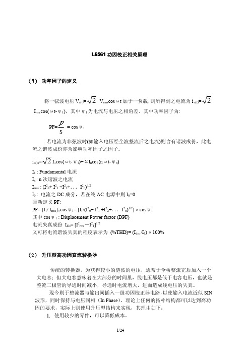
ST 公司生产的L6561 是采用变频峰值电流控制方式的PFC 控制器,Boost PFC 转换器工作在电感电流临界连续模式(CRM),主开关管零电流、零电压开通。
它的内部电路和典型应用分别如图1(a)、(b)所示。
芯片内部电路包
括电压放大器VA、乘法器、电流过流检测比较器、触发器和驱动电路等。
转
换器的输出电压Uo 由VA 的反相输人端INV 通过分压电阻采样,电压补偿网
络(图1(b)中为电容C1)跨接在INV 和、VA 输出端COMP;MULT 采样
输入整流电压信号,并与COMP 信号相乘、乘法器的输出作为峰值电流基准。
Boost 转换器开关V 的电流采样信号(CS 端采样)上升到该值时,电流比较器CA 及触发器翻转。
驱动器输出端GD 输低电平,令V 关断。
在V 关断期间,
电感电流iL 下降,ZCD 通过输人滤波电感L,的辅助绕组。
检测其两端电压
μL,当捡测佶号电压下降到接近于零(2.1V) 时,则认为电感电流已经下降到零,电流过零捡测比较器翻转,GD 端再次输出高电平,开关管V 实现零电流零电压
开通。
电感L 辅助绕组间时也为L6561 芯片提供工作电源。
图1 L656l 控制的CRM Boost PFC 转换器
tips:感谢大家的阅读,本文由我司收集整编。
仅供参阅!。
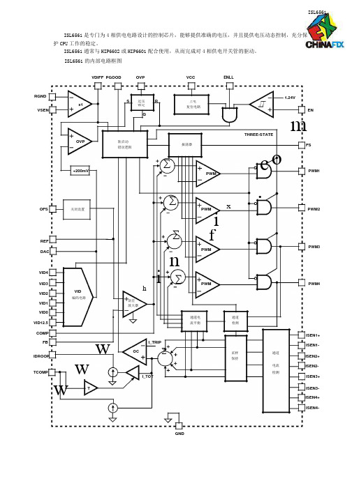
ISL6561ISL6561是专门为4相供电电路设计的控制芯片,能够提供准确的电压,并且提供电压动态控制,充分保 护CPU 工作的稳定。
ISL6561通常与HIP6602或HIP6601配合使用,从而完成对4相供电开关管的驱动。
ISL6561的内部电路框图VDIFF PGOODOVPVCCENLLRGNDS过压 R1.24Vx1上电VSEN锁定复位电路ENQmTHREE-STATEOVP软启动振荡器FS 错误逻辑o+200mV∑PWMcPWM1∑.OFS关闭设置xPWM2PWM∑iREFfDACPWMPWM3nVID4i∑VID3PWMPWM4VID2VIDhVID1 编码电路误差放大器VID0.VID12.5通道电 通道流平衡检测COMPwISEN1+ FBI_TRIPISEN1-IDROOPwOC∑采样 通道ISEN2+保持电流ISEN2- TCOMPwI_TOT检测ISEN3+TISEN3- ISEN4+ISEN4-GNDISL6561的各引脚功能引脚号引脚名称引脚功能1 VID42 VID3此时无控制信号,模式CPU”无“则工作在,个引脚均悬空 6 电压模式识别端。
若这 CPU3 VID2输出4 VID15 VID06 VID12.57,12,19GND 接地端m 37,408 OFS 可调直流偏压输入补偿端9 TCOMP 温度补偿输入端o10 DAC 译码器输出端 c11 REF 误差放大器正相输入端.13 FB 输出电压反馈信号输入端14 IDROOP 均衡电流检测输出端x15 COMP 误差放大器输出端i16 VDIFF 内部放大器输出端 f17 VSEN 电压反馈检测输入端18 RGND 集成电路接地端20 PWM3 3 控制信号输出端 PWM a21 ISEN3+ 3 电流检测正相输入端22 -ISEN3 3 电流检测反相输入端n23 -ISEN1 1 电流检测反相输入端24 ISEN1+ 1 电流检测正相输入端h25 PWM1 1 控制信号输出端 PWM26 PWM2 2 控制信号输出端 PWMc27 ISEN2+ 2 电流检测正相输入端.28 -ISEN2 2 电流检测反相输入端29 -ISEN4 4 电流检测正相输入端30 ISEN4+ 4 电流检测反相输入端w31 PWM4 4 控制信号输出端 PWM33 VCC 供电电压输入端w33 EN 使能控制端34 ENLL 逻辑使能控制端w35 GND 接地端36 FS 开关频率设置端38 OVP 过压保护端39 PGOOD 信号输入端 GOOG POWERISL6561的针脚封装图G N DP G O O DO V PG N DF SG N DE N L LE NV C CP W M 440 39 38 37 36 35 34 33 32 31VID4 130ISEN4+VID3 229 ISEN4-VID2 3 28 ISEN2-VID1 4 ISEN2+27VID0 5 26 PWM2VID12.5 625 PWM1GND 724 ISEN1+OFS 8 23 ISEN1-TCOMP 922 ISEN3-DAC 1021 ISEN3+o m11121314 15 16R E F G N DF BI D R O O PC O M VD I F FISL6561控制端电平与输出电压的关系VID4VID3VID2VID10 0 0 0 0 0 0 0n111 111 1 1 111h1111i 111111c111111.w11 10 11111111w111 w1110 01 1 0 0 1 1 0 0 1 0 1 1 1 0 1 1 1 0 1 1 1 0 1 1 1 0 1 0 1 0 1 0 10 1 0 1117 181920cV S E NR G N DG N DP M 3.1x0 f1 a0 1 1 1 0 0 1 0 0 1 1 1 0 0 1 0 0 1 1 1 0 0 1 0 0 1 1 1 0 0 1 0 0 1 1 1 0 0 1 0 0 1 1 1 0 0 1 0(V )输出电压1.0625 1.0750 1.0875关闭 关闭1.1000 1.1125 1.1250 1.1375 1.1500 1.1625 1.1750 1.1875 1.2000 1.2125 1.2250 1.2475 1.2500 1.2625 1.2750 1.2875 1.3000 1.3125 1.3250 1.33751.3500 1.3625续表VID4 VID31 01 01 01 01 01 01 01 00 10 10 10 10 10 10 10 10 10 10 1w ww VID2 VID1 VID0 VID12.5 (V)输出电压0 1 1 1 1.3750m0 1 1 0 1.3875 0 1 0 1 o 1.4000 0 1 0 0 1.4125 0 0 1 1 c 1.4250 0 0 1 0 1.4375.0 0 0 1 1.45000 0 0 x 0 1.46251 1 1 1 1.4750 1 1 1 i 0 1.4875 1 1 0 f 1 1.5000 1 1 0 0 1.5125a1 0 1 1 1.5250 1 0 n 1 0 1.5375 1 0 0 1 1.5500i1 0 0 0 1.5625 0 h 1 1 1 1.5750 0 1 1 0 1.5875 0 1 0 1 1.600 c.ISL6561的典型应用电路图+12VVCCBOOTVINUGATEPVCCPHASEHIP6601BPWM DRIVERLGATENTC+5V GNDTHERMISTORFBCOMP REF+12VomIDROOPDACVCC BOOTVINVDIFFcVSENVCCRGND.VIDPGOODENLLUGATEPGOODISL6561PVCCPHASEVID4ISEN1+PWMHIP6601BISEN1- DRIVERVID3LGATEPWM1xVID2PWM2GNDiVID1ISEN2+aISEN2-VID0+12VPWM3VIN VID12.5ISEN3+PISEN3-VCCLOADnOFSPWM4BOOTFSISEN4+ hUGATEISEN4-i PVCCPHASERT TCOMP GNDENcPWM HIP6601BDRIVER LGATE.+12VGNDw+12VwVCCVINBOOTwUGATEPVCCPHASEHIP6601BPWMDRIVERLGATEGND。

全尺寸液晶电视和等离子电视 电源解决方案目录传统电源:60W 开关电源(SMPS )(<20吋) 200W SMPS (最大 30-32吋)谐振电源:70W SMPS (<20吋) 180W SMPS (最大30吋) 500W SMPS (最大50吋 LCD-TV, 42吋 PDP-TV)60W 液晶电视(LCD-TV) 电源: 块图•工作模式接近CCM 和DCM之间的界 限:可变工作频率Vac电源单元EMI 滤波器和 桥接整流器 +12V•导通时零压开关/零 流开关 •EMI干扰不强 •可变扩展频谱 •启用待机功能先进的PWM控 制器反馈60W LCD-TV 电源: 技术规格宽输入电压: 90-265VAC 单输出电压 (Vout): Vout 电流 说明12V 5A 器件内的精确的过流和过压保护电路可 以选装。
.总输出功率: 60W60W LCD-TV 电源:电路图L656560W LCD-TV 电源: 测试报告负载效率测试负载 输出 全负载 (FL) 待机 无负载 测试结果 输入电压 全负载效率 待机 90V 100V 240V 264V 81.7% 83.2% 87.0% 87.4% 输入功率 无负载 12V 5A 0.0416A (0.5W) 0A一台60W LCD-TV 电源L6565: 准谐振开关电源控制器• 电流式准谐振PWM 控制器 • 微功率启动电流 (40µA 典型) • 小静态电流 (3mA典型值) • 谐振工作/外部数据同步ZCD 输 入 • 频率反馈功能 • 线路电压正向功能 • 逐脉冲过流保护 • 第二个电流级和打嗝模式工作 • 禁用功能 •电流读取上的内部RC滤波器 • 封装: Minidip 和SO8准谐振(QR)转换 : 准谐振概念Llk & CdLp Lm Ls VoutLp & C d VDSVDS @ Vin2 >VinCinLlk VRVin2VinVinCd VDSNO ZVS! Ip IPKs Pri Sec tZVSIs @ Vin2 >Vin工作模式接近CCM和DCM之间的界限:可 变工作频率 导通时零压开关(ZVS)/零流开关(ZCS) EMI干扰不强 可变扩展频谱IPKpIp @ Vin2 >VinTON T = 1/ fswTFWTvZVS 条件: Vin ≤ VR200W LCD-TV 电源: 块图•PFC(功率因数校正器)电源VacEMI 滤波器 和桥接整流 器200W 临界控制模 式,具备ZCD(零流 检测)功能,注重成 本效益 •主变换器 200W逆向变换器, 用于中等尺寸的 LCD-PDP/TV应用 •备用变换器 10W 逆变换器,内 置场效应MOS控制 器,和关断电路+24V+12V PFC+PWM+Aux L6562+L5991 +L6590 DC DC 变换器 +5V反馈 +5V 备 用变换200W LCD-TV 电源:技术规格5V 输出使用的DC-DC 变换器可以选择。
L6561 应用笔记中文版L6561 ,增强版的临界模式功率因数校正器TM(临界模式)技术广泛应用于低功率产品的功率因数校正,例如灯具镇流器,视频终端控制电路。
L6561是后期针对这个市场推出的产品,不但符合要求而且是一款低价的功率因数校正器。
基于一个非常好的电路架构,L6561展现出非常优越的性能,而且应用领域更为广泛。
介绍传统的单级离线式转换电路,都是由一个全桥整流和一个电容滤波构成。
通过交流主线电源获得一个未校准的直流电压,滤波电容必须足够大以便可以得到一个纹波电压比较小的直流电压,这就意味着在大多数时间内,电容上的电压高于输入AC电源线电压,这就意味着,全桥整流电路仅在输入线电压每半周期内(因为有整流桥的存在,整流后的每个周期相当于AC电源的半个周期),工作很短的时间。
使得从电网输入的电流变成很窄的脉冲波形,其幅度是同等直流电压下电流幅度的5-10倍。
许多缺点因此而产生:过高的峰值电流和RMS电流比,使得交流电网电压畸变,在三相线输电电网中,使中性线过电流,总之,会使电网的输电能力减弱。
关于这项指标,可以参考谐波允许量标准EN61000-3-2,或功率因数PF,有功功率(传送到输出端的功率)和输入视在功率(线电压真有效值和线电流真有效值的乘积)的比值,功率因数PF是最直观的。
传统的输入电容滤波电路功率因数很低(05-0.7),并且谐波含量很高。
图1. L6561内部模块图由于使用了开关技术,功率因数矫正器(PFC)位于整流桥和滤波电容之间,从电源获取一个准正弦波电流,与线电压同步,功率因数变得非常接近1(可以超过0.99),上述的缺点得以消除。
从理论上来讲,任何开关拓扑技术都可以用来获取一个高功率因数,但是,实际应用中,升压拓扑是一种最流行的方式,因为它有以下优势:1)主要是,因为升压电路所需的元件最少,因此这种方式最便宜。
还有:2)由于升压电感位于整流桥和开关之间,引起的电流di/dt比较低,可以使输入产生的噪音最小化,可以减少输入EMI滤波元件。
December 2010Doc ID 16047 Rev 31/49L6563HHigh voltage start-up transition-mode PFCFeatures■On-board 700 V start-up source ■Tracking boost function■Fast “bidirectional” input voltage feedforward (1/V 2 correction)■Interface for cascaded converter's PWM controller■Remote ON/OFF control■Accurate adjustable output overvoltage protection■Protection against feedback loop disconnection (latched shutdown)■Inductor saturation protection ■Low (≤ 100 µA) start-up current ■ 6 mA max. operating bias current■1% (@ T J = 25 °C) internal reference voltage ■-600/+800 mA totem pole gate driver with active pull-down during UVLOApplications■PFC pre-regulators for:–Hi-end AC-DC adapter/charger–IEC61000-3-2 or JEIT A-MITI compliant SMPS, in excess of 400 W ■SMPS for LED luminairesContents L6563HContents1Description . . . . . . . . . . . . . . . . . . . . . . . . . . . . . . . . . . . . . . . . . . . . . . . . . 62Maximum ratings . . . . . . . . . . . . . . . . . . . . . . . . . . . . . . . . . . . . . . . . . . . . 72.1Absolute maximum ratings . . . . . . . . . . . . . . . . . . . . . . . . . . . . . . . . . . . . . 72.2Thermal data . . . . . . . . . . . . . . . . . . . . . . . . . . . . . . . . . . . . . . . . . . . . . . . 7 3Pin connection . . . . . . . . . . . . . . . . . . . . . . . . . . . . . . . . . . . . . . . . . . . . . . 8 4Electrical characteristics . . . . . . . . . . . . . . . . . . . . . . . . . . . . . . . . . . . . 11 5Typical electrical performance . . . . . . . . . . . . . . . . . . . . . . . . . . . . . . . . 156Application information . . . . . . . . . . . . . . . . . . . . . . . . . . . . . . . . . . . . . 246.1Overvoltage protection . . . . . . . . . . . . . . . . . . . . . . . . . . . . . . . . . . . . . . . 246.2Feedback failure protection (FFP) . . . . . . . . . . . . . . . . . . . . . . . . . . . . . . 256.3Voltage feedforward . . . . . . . . . . . . . . . . . . . . . . . . . . . . . . . . . . . . . . . . . 256.4THD optimizer circuit . . . . . . . . . . . . . . . . . . . . . . . . . . . . . . . . . . . . . . . . 286.5Tracking boost function . . . . . . . . . . . . . . . . . . . . . . . . . . . . . . . . . . . . . . . 296.6Inductor saturation detection . . . . . . . . . . . . . . . . . . . . . . . . . . . . . . . . . . 316.7Power management/housekeeping functions . . . . . . . . . . . . . . . . . . . . . . 326.8High-voltage start-up generator . . . . . . . . . . . . . . . . . . . . . . . . . . . . . . . . 35 7Application examples and ideas . . . . . . . . . . . . . . . . . . . . . . . . . . . . . . 39 8Package mechanical data . . . . . . . . . . . . . . . . . . . . . . . . . . . . . . . . . . . . 45 9Ordering codes . . . . . . . . . . . . . . . . . . . . . . . . . . . . . . . . . . . . . . . . . . . . 47 10Revision history . . . . . . . . . . . . . . . . . . . . . . . . . . . . . . . . . . . . . . . . . . . 482/49Doc ID 16047 Rev 3L6563H List of table List of tableTable 1.Absolute maximum ratings. . . . . . . . . . . . . . . . . . . . . . . . . . . . . . . . . . . . . . . . . . . . . . . . . . 7 Table 2.Thermal data. . . . . . . . . . . . . . . . . . . . . . . . . . . . . . . . . . . . . . . . . . . . . . . . . . . . . . . . . . . . . 7 Table 3.Pin description . . . . . . . . . . . . . . . . . . . . . . . . . . . . . . . . . . . . . . . . . . . . . . . . . . . . . . . . . . . 8 Table 4.Electrical characteristics. . . . . . . . . . . . . . . . . . . . . . . . . . . . . . . . . . . . . . . . . . . . . . . . . . . 11 Table 5.Summary of L6563H idle states . . . . . . . . . . . . . . . . . . . . . . . . . . . . . . . . . . . . . . . . . . . . . 38 Table 6.SO16 mechanical data. . . . . . . . . . . . . . . . . . . . . . . . . . . . . . . . . . . . . . . . . . . . . . . . . . . . 45 Table 7.Ordering information. . . . . . . . . . . . . . . . . . . . . . . . . . . . . . . . . . . . . . . . . . . . . . . . . . . . . . 47 Table 8.Document revision history . . . . . . . . . . . . . . . . . . . . . . . . . . . . . . . . . . . . . . . . . . . . . . . . . 48Doc ID 16047 Rev 33/49List of figure L6563H List of figureFigure 1.Block diagram. . . . . . . . . . . . . . . . . . . . . . . . . . . . . . . . . . . . . . . . . . . . . . . . . . . . . . . . . . . . 1 Figure 2.Pin connection . . . . . . . . . . . . . . . . . . . . . . . . . . . . . . . . . . . . . . . . . . . . . . . . . . . . . . . . . . . 8 Figure 3.Typical system block diagram. . . . . . . . . . . . . . . . . . . . . . . . . . . . . . . . . . . . . . . . . . . . . . . 10 Figure 4.IC consumption vs VCC . . . . . . . . . . . . . . . . . . . . . . . . . . . . . . . . . . . . . . . . . . . . . . . . . . . 15 Figure 5.IC consumption vs TJ. . . . . . . . . . . . . . . . . . . . . . . . . . . . . . . . . . . . . . . . . . . . . . . . . . . . . 15 Figure 6.Vcc Zener voltage vs TJ. . . . . . . . . . . . . . . . . . . . . . . . . . . . . . . . . . . . . . . . . . . . . . . . . . . 15 Figure 7.Start-up and UVLO vs TJ . . . . . . . . . . . . . . . . . . . . . . . . . . . . . . . . . . . . . . . . . . . . . . . . . . 15 Figure 8.Feedback reference vs TJ . . . . . . . . . . . . . . . . . . . . . . . . . . . . . . . . . . . . . . . . . . . . . . . . . 16 Figure 9.E/A output clamp levels vs TJ. . . . . . . . . . . . . . . . . . . . . . . . . . . . . . . . . . . . . . . . . . . . . . . 16 Figure 10.UVLO saturation vs TJ . . . . . . . . . . . . . . . . . . . . . . . . . . . . . . . . . . . . . . . . . . . . . . . . . . . . 16 Figure 11.OVP levels vs TJ . . . . . . . . . . . . . . . . . . . . . . . . . . . . . . . . . . . . . . . . . . . . . . . . . . . . . . . . 16 Figure 12.Inductor saturation threshold vs TJ. . . . . . . . . . . . . . . . . . . . . . . . . . . . . . . . . . . . . . . . . . . 17 Figure 13.Vcs clamp vs TJ . . . . . . . . . . . . . . . . . . . . . . . . . . . . . . . . . . . . . . . . . . . . . . . . . . . . . . . . . 17 Figure 14.ZCD sink/source capability vs TJ . . . . . . . . . . . . . . . . . . . . . . . . . . . . . . . . . . . . . . . . . . . . 17 Figure 15.ZCD clamp level vs TJ . . . . . . . . . . . . . . . . . . . . . . . . . . . . . . . . . . . . . . . . . . . . . . . . . . . . 17 Figure 16.TBO clamp vs TJ . . . . . . . . . . . . . . . . . . . . . . . . . . . . . . . . . . . . . . . . . . . . . . . . . . . . . . . . 18 Figure 17.VVFF - VTBO dropout vs TJ. . . . . . . . . . . . . . . . . . . . . . . . . . . . . . . . . . . . . . . . . . . . . . . . 18 Figure 18.IINV - ITBO current mismatch vs TJ. . . . . . . . . . . . . . . . . . . . . . . . . . . . . . . . . . . . . . . . . . 18 Figure 19.IINV - ITBO mismatch vs ITBO current. . . . . . . . . . . . . . . . . . . . . . . . . . . . . . . . . . . . . . . . 18 Figure 20.R discharge vs TJ. . . . . . . . . . . . . . . . . . . . . . . . . . . . . . . . . . . . . . . . . . . . . . . . . . . . . . . . 19 Figure 21.Line drop detection threshold vs TJ . . . . . . . . . . . . . . . . . . . . . . . . . . . . . . . . . . . . . . . . . . 19 Figure 22.VMULTpk - VVFF dropout vs TJ. . . . . . . . . . . . . . . . . . . . . . . . . . . . . . . . . . . . . . . . . . . . . 19 Figure 23.PFC_OK threshold vs TJ . . . . . . . . . . . . . . . . . . . . . . . . . . . . . . . . . . . . . . . . . . . . . . . . . . 19 Figure 24.PFC_OK FFD threshold vs TJ . . . . . . . . . . . . . . . . . . . . . . . . . . . . . . . . . . . . . . . . . . . . . . 20 Figure 25.PWM_LATCH high saturation vs TJ. . . . . . . . . . . . . . . . . . . . . . . . . . . . . . . . . . . . . . . . . . 20 Figure 26.RUN threshold vs TJ. . . . . . . . . . . . . . . . . . . . . . . . . . . . . . . . . . . . . . . . . . . . . . . . . . . . . . 20 Figure 27.PWM_STOP low saturation vs TJ . . . . . . . . . . . . . . . . . . . . . . . . . . . . . . . . . . . . . . . . . . . 20 Figure 28.Multiplier characteristics @ VFF = 1 V . . . . . . . . . . . . . . . . . . . . . . . . . . . . . . . . . . . . . . . . 21 Figure 29.Multiplier characteristics @ VFF = 3 V . . . . . . . . . . . . . . . . . . . . . . . . . . . . . . . . . . . . . . . . 21 Figure 30.Multiplier gain vs TJ . . . . . . . . . . . . . . . . . . . . . . . . . . . . . . . . . . . . . . . . . . . . . . . . . . . . . . 21 Figure 31.Gate drive clamp vs TJ. . . . . . . . . . . . . . . . . . . . . . . . . . . . . . . . . . . . . . . . . . . . . . . . . . . . 21 Figure 32.Gate drive output saturation vs TJ . . . . . . . . . . . . . . . . . . . . . . . . . . . . . . . . . . . . . . . . . . . 22 Figure 33.Delay to output vs TJ . . . . . . . . . . . . . . . . . . . . . . . . . . . . . . . . . . . . . . . . . . . . . . . . . . . . . 22 Figure 34.Start-up timer period vs TJ. . . . . . . . . . . . . . . . . . . . . . . . . . . . . . . . . . . . . . . . . . . . . . . . . 22 Figure 35.HV start voltage vs TJ. . . . . . . . . . . . . . . . . . . . . . . . . . . . . . . . . . . . . . . . . . . . . . . . . . . . . 22 Figure 36.VCC restart voltage vs TJ. . . . . . . . . . . . . . . . . . . . . . . . . . . . . . . . . . . . . . . . . . . . . . . . . . 23 Figure 37.HV breakdown voltage vs TJ . . . . . . . . . . . . . . . . . . . . . . . . . . . . . . . . . . . . . . . . . . . . . . . 23 Figure 38.Output voltage setting, OVP and FFP functions: internal block diagram . . . . . . . . . . . . . . 24 Figure 39.Voltage feedforward: squarer-divider (1/V2) block diagram and transfer characteristic . . 26 Figure 40.RFF·CFF as a function of 3rd harmonic distortion introduced in the input current. . . . . . . 27 Figure 41.THD optimizer circuit . . . . . . . . . . . . . . . . . . . . . . . . . . . . . . . . . . . . . . . . . . . . . . . . . . . . . 28 Figure 42.THD optimization: standard TM PFC controller (left side) and L6563H (right side) . . . . . . 29 Figure 43.Tracking boost block. . . . . . . . . . . . . . . . . . . . . . . . . . . . . . . . . . . . . . . . . . . . . . . . . . . . . . 31 Figure 44.Tracking output voltage vs Input voltage characteristic with TBO . . . . . . . . . . . . . . . . . . . 31 Figure 45.Effect of boost inductor saturation on the MOSFET current and detection method . . . . . . 32 Figure 46.Interface circuits that let dc-dc converter's controller IC drive L6563H in burst mode . . . . 33 Figure 47.Interface circuits that let the L6563H switch on or off a PWM controller. . . . . . . . . . . . . . . 33 Figure 48.Interface circuits for power up sequencing when dc-dc has the SS function . . . . . . . . . . . 34 4/49Doc ID 16047 Rev 3L6563H List of figure Figure 49.Interface circuits for actual power-up sequencing (master PFC) . . . . . . . . . . . . . . . . . . . . 34 Figure 50.Brownout protection (master PFC). . . . . . . . . . . . . . . . . . . . . . . . . . . . . . . . . . . . . . . . . . . 35 Figure 51.High-voltage start-up generator: internal schematic. . . . . . . . . . . . . . . . . . . . . . . . . . . . . . 35 Figure 52.Timing diagram: normal power-up and power-down sequences . . . . . . . . . . . . . . . . . . . . 36 Figure 53.High-voltage start-up behaviour during latch-off protection . . . . . . . . . . . . . . . . . . . . . . . . 37 Figure 54.High-voltage start-up managing the dc-dc output short-circuit. . . . . . . . . . . . . . . . . . . . . . 37 Figure 55.Demonstration board EVL6563H-100W, wide-range mains: electrical schematic . . . . . . . 39 Figure 56.L6563H 100 W TM PFC evaluation board: compliance to EN61000-3-2 standard . . . . . . 40 Figure 57.L6563H 100 W TM PFC evaluation board: compliance to JEITA-MITI standard . . . . . . . . 40 Figure 58.L6563H 100 W TM PFC evaluation board: input current waveform @230-50 Hz - 100 W load . . . . . . . . . . . . . . . . . . . . . . . . . . . . . . . . . . . . . . . . . . . . . . . . . . . . . . . . . . . . . . . . . . . . . . 40 Figure 59.L6563H 100W TM PFC evaluation board: input current waveform @100 V-50 Hz - 100 W . load . . . . . . . . . . . . . . . . . . . . . . . . . . . . . . . . . . . . . . . . . . . . . . . . . . . . . . . . . . . . . . . . . . . . . . 40 Figure 60.EVL90WADP-LLCSR 90W adapter with SRK2000 demonstration board: electrical schematic . . . . . . . . . . . . . . . . . . . . . . . . . . . . . . . . . . . . . . . . . . . . . . . . . . . . . . . . . . . . . . . . . . . . . . 41 Figure 61.EV150WAIO-LLCSR 150W-12V Adapter with L6563H, L6599A, SRK2000: electrical sche-matic . . . . . . . . . . . . . . . . . . . . . . . . . . . . . . . . . . . . . . . . . . . . . . . . . . . . . . . . . . . . . . . . . . . . . . 42 Figure 62.EVL6563H -250W TM PFC demonstration board : electrical schematic . . . . . . . . . . . . . . 43 Figure 63.EVL6599A-90WADP 90W Adapter demonstration board: electrical schematic. . . . . . . . . 44 Figure 64.SO16 mechanical data. . . . . . . . . . . . . . . . . . . . . . . . . . . . . . . . . . . . . . . . . . . . . . . . . . . . 46Doc ID 16047 Rev 35/49Description L6563H 1 DescriptionThe L6563H is a current-mode PFC controller operating in transition mode (TM) whichembeds the same features existing in the L6563S with the addition of a high voltage start-upsource. These functions make the IC especially suitable for applications that have to becompliant with energy saving regulations and where the PFC pre-regulator works as themaster stage.The highly linear multiplier, along with a special correction circuit that reduces crossoverdistortion of the mains current, allows wide-range-mains operation with an extremely lowTHD even over a large load range.The output voltage is controlled by means of a voltage-mode error amplifier and an accurate(1% @Tj = 25 °C) internal voltage reference. Loop's stability is optimized by the voltagefeedforward function (1/V2 correction), which in this IC uses a proprietary technique thatconsiderably improves line transient response as well in case of mains both drops andsurges (“bidirectional”).Additionally, the IC provides the option for tracking boost operation, i.e. the output voltage ischanged tracking the mains voltage.The device includes disable functions suitable for remote ON/OFF control too.In addition to an over voltage protection able to keep the output voltage under control duringtransient conditions, the IC is provided also with a protection against feedback loop failuresor erroneous settings. Other on-board protection functions allow that brownout conditionsand boost inductor saturation can be safely handled.An interface with the PWM controller of the DC-DC converter supplied by the PFC pre-regulator is provided: the purpose is to stop the operation of the converter in case ofanomalous conditions for the PFC stage (feedback loop failure, boost inductor's coresaturation, etc.) and to handle the PFC stage in case of light load for the DC-DC converter,to make it easier to comply with energy saving regulations (Blue Angel, EnergyStar,Energy2000, etc.).The totem-pole output stage, capable of 600 mA source and 800 mA sink current, is suitablefor big MOSFET or IGBT drive. This, combined with the other features and the possibility tooperate with ST's proprietary fixed-off-time control, makes the device an excellent solutionfor SMPS up to 400 W that need to be compliant with EN61000-3-2 and JEIT A-MITIstandards.6/49Doc ID 16047 Rev 3L6563H Maximum ratingsDoc ID 16047 Rev 37/492 Maximum ratings2.1Absolute maximum ratings2.2 Thermal dataTable 1.Absolute maximum ratingsSymbol Pin ParameterValue Unit V HVS 9Voltage range (referred to ground)-0.3 to 700VI HVS 9Output currentSelf-limited I HVS Vcc 16IC supply voltage (Icc = 20 mA)self-limited V ---1, 3, 7Max. pin voltage (I pin =1 mA)Self-limited V ---2, 4 to 6, 8, 11, 12Analog inputs and outputs-0.3 to 8V I PWM_STOP11Max. sink current3mAI ZCD13Zero current detector max. current-10 (source)10 (sink)mATable 2.Thermal dataSymbol ParameterValue Unit R thJA Max. thermal resistance, junction-to-ambient 120°C/W Ptot Power dissipation @T A = 50 °C 0.75W T J Junction temperature operating range -40 to 150°C T stgStorage temperature-55 to 150°CPin connection L6563H8/49Doc ID 16047 Rev 33 Pin connectionTable 3.Pin descriptionn°NameFunction1INVInverting input of the error amplifier. The information on the output voltage of the PFC pre-regulator is fed into the pin through a resistor divider.The pin normally features high impedance but, if the tracking boost function is used, an internal current generator programmed by TBO (pin 6) is activated. It sinks current from the pin to change the output voltage so that it tracks the mains voltage.2COMPOutput of the error amplifier. A compensation network is placed between this pin and INV (pin 1) to achieve stability of the voltage control loop and ensure high power factor and low THD. T o avoid uncontrolled rise of the output voltage at zero load, when the voltage on the pin falls below 2.4 V the gate driver output is inhibited (burst-mode operation).3MULTMains input to the multiplier. This pin is connected to the rectified mains voltage via a resistor divider and provides the sinusoidal reference to the current loop. The voltage on this pin is used also to derive the information on the RMS mains voltage.4CSInput to the PWM comparator. The current flowing in the MOSFET is sensed through a resistor, the resulting voltage is applied to this pin and compared with an internal reference to determine MOSFET’s turn-off.A second comparison level at 1.7 V detects abnormal currents (e.g. due to boost inductor saturation) and, on this occurrence, activates a safety procedure that temporarily stops the converter and limits the stress of the power components.5VFFSecond input to the multiplier for 1/V 2 function. A capacitor and a parallel resistor must beconnected from the pin to GND. They complete the internal peak-holding circuit that derives the information on the RMS mains voltage. The voltage at this pin, a dc level equal to the peak voltage on pin MULT (3), compensates the control loop gain dependence on the mains voltage. Never connect the pin directly to GND but with a resistor ranging from 100 k Ω (minimum) to 2 M Ω (maximum).6TBOT racking boost function. This pin provides a buffered VFF voltage. A resistor connectedbetween this pin and GND defines a current that is sunk from pin INV (1). In this way, the output voltage is changed proportionally to the mains voltage (tracking boost). If this function is not used leave this pin open.L6563H Pin connectionDoc ID 16047 Rev 39/497PFC_OKPFC pre-regulator output voltage monitoring/disable function. This pin senses the outputvoltage of the PFC pre-regulator through a resistor divider and is used for protection purposes. If the voltage on the pin exceeds 2.5 V the IC stops switching and restarts as the voltage on the pin falls below 2.4 V . However, if at the same time the voltage of the INV pin falls below 1.66V , a feedback failure is assumed. In this case the device is latched off and the PWM_LA TCH (8) pin is asserted high. Normal operation can be resumed only by cycling Vcc bringing its value lower than 6V before to move up to Turn on threshold.If the voltage on this pin is brought below 0.23 V the IC is shut down. T o restart the IC the voltage on the pin must go above 0.27 V . This can be used as a remote on/off control input.8PWM_LA TCHOutput pin for fault signaling. During normal operation this pin features high impedance. If a feedback failure is detected (PFC_OK > 2.5 V & INV < 1.66V) the pin is asserted high.Normally, this pin is used to stop the operation of the dc-dc converter supplied by the PFC pre-regulator by invoking a latched disable of its PWM controller. If not used, the pin is left floating.9HVSHigh-voltage start-up. The pin, able to withstand 700 V , is to be tied directly to the rectified mains voltage. A 1 mA internal current source charges the capacitor connected between pin Vcc (16) and pin GND (14) until the voltage on the pin Vcc reaches the start-up threshold, then it is shut down. Normally, the generator is re-enabled when the Vcc voltage falls below 6 V to ensure a low power throughput during short circuit. Otherwise, when a latched protection is tripped the generator is re-enabled as Vcc reaches the UVLO threshold to keep the latch supplied.10N.C.Not internally connected. Provision for clearance on the PCB to meet safety requirements.11PWM_STOPOutput pin for fault signaling. During normal operation this pin features high impedance. If the IC is disabled by a voltage below 0.8 V on pin RUN (12) the voltage on the pin is pulled to ground. Normally, this pin is used to temporarily stop the operation of the dc-dc convertersupplied by the PFC pre-regulator by disabling its PWM controller. A typical usage of thisfunction is brownout protection in systems where the PFC pre-regulator is the master stage. If not used, the pin is left floating.12RUNRemote ON/OFF control. A voltage below 0.8 V shuts down (not latched) the IC and brings its consumption to a considerably lower level. PWM_STOP is asserted low. The IC restarts as the voltage at the pin goes above 0.88V . Connect this pin to pin VFF (5) either directly or through a resistor divider to use this function as brownout (AC mains undervoltage) protection.13ZCD Boost inductor’s demagnetization sensing input for transition-mode operation. A negative-going edge triggers MOSFET’s turn-on.14GND Ground. Current return for both the signal part of the IC and the gate driver.15GDGate driver output. The totem pole output stage is able to drive power MOSFET’s and IGBT’s with a peak current of 600 mA source and 800 mA sink. The high-level voltage of this pin is clamped at about 12 V to avoid excessive gate voltages.16VccSupply voltage of both the signal part of the IC and the gate driver. Sometimes a small bypass capacitor (0.1 µF typ.) to GND might be useful to get a clean bias voltage for the signal part of the IC.Table 3.Pin description (continued)n°NameFunctionPin connection L6563H10/49Doc ID 16047 Rev 3分销商库存信息:STML6563HTR L6563H EVL6563H-100W。
L6561功率因数校正1■■特征非常精确的可调输出过电压保护微功率启动电流(50µATYP.)非常低的电源电流(4mA TYP.)内部启动定时器片上电流检测滤波器禁止功能1%精密(@ T j= 25°C)内部参考电压过渡模式操作图腾柱输出电流:±400mADIP-8/SO-8套餐图1.软件包DIP-8SO-8■订购代码表1.部件号L6561L6561DL6561D013TR包装DIP-8SO-8带卷■■■■■■■2描述L6561是改良版的L6560 stan-dard功率因数修正器.完全兼容with the standard version, it has a superior perfor-mant乘数使设备的工作能力,在宽输入电压范围的应用ing(从85V到265V)了一个良好的THD.此外当前开始向上在数已减少tensmA和禁用的功能已经实现,教育署对ZCD针,保证较低的电流消费模式下的立场.图2.框图COMP2INV12.5V-+在混合BCD技术变现,该芯片提供以下好处:–微功率启动电流– 1%高精度内部参考电压– (Tj = 25°C)–软输出过电压保护–无需外部低通滤波器需要对电流,租金感–非常低的静态电流最低,es功耗图腾柱输出级驱动能力一个电源MOS或源IGBT和汇电流租金的±400mA.设备运行中tran-sition模式,它是电子灯优化镇流管应用,AC-DC适配器和SMPS.MULT3440KCSMULTIPLIERVOLTAGE REGULATOR OVER-VOLTAGEDETECTION-+5pFV 8VINTERNALSUPPLY 7VR1+UVLORSDRIVERQ720VGDR2V2.1V1.6VZERO CURRENTDETECTORSTARTER6GNDJune 2004-+-DISABLE5ZCDREV的. 161/13L6562中文数据手册,L6562 Datasheet PDF,L6562芯片中文资料【L6561表2.绝对最大额定值符号I VccI GDINV, COMPMULTCSZCDP totT jT stg针871, 2, 345I q+ I Z; (I GD= 0)图腾柱输出电流(2µs) 峰值模拟输入和输出电流检测输入零电流检测器功率消耗@T amb= 50 °C结温工作范围贮藏温度(DIP-8)(SO-8)参数价值30±700-0.3到7-0.3到750(源)-10(汇)10.65-40到150-55到150单位mAmAVVmAmAWW°C°C图3.引脚连接(顶视图)INV COMP MULTCS 1234DIP88765V CCGDGNDZCD热数据表3.符号R th j-amb参数结到环境的热阻苏8150MINIDIP100单位°C/W表4.引脚说明N. 12345 6 78名称INVCOMPMULTCSZCDGNDGDV CC功能反相误差放大器的输入.一个电阻分压器的输出之间连接稳压这一点,提供电压反馈.误差放大器的输出.一个反馈补偿网络之间设置这个引脚和INV引脚.乘法器的输入阶段.一个电阻分压器连接到这个引脚的整流电源.一个电压信号,比例整流电源,出现在该引脚.输入到控制回路比较.该感应电流通过电阻和由此产生的电压施加到该管脚.零电流检测输入.如果是连接到GND,设备被禁用.当前返回驱动器和控制电路.门驱动器输出.一个推挽输出级可驱动峰值目前电源MOS400mA(源和接收器).电源电压驱动器和控制电路.(1)参数由设计保证,而不是在生产测试.2/13L6561电气特性表5.(V CC = 14.5V; T amb = -25°C 到125°C ,除非另有规定)符号V CC V CC ON V CC OFF Hys I START-UI q I CCIqV ZV INV针88888888881齐纳电压电压反馈输入门槛线路调整I INV G V GB I COMPV COMP221电流输入偏置电压增益增益带宽源电流灌电流上钳位电压低钳位电压乘第V MULT ∆VCS-----------------∆VmultKV CS I CS t d (H-L)4444V ZCD53线性工作电压输出最大.斜坡V MULT 从= 0V 到0.5V V COMP =上钳位电压V MULT = 1V VCOMP= 4V V MULT = 2.5VV COMP =上钳位电压V OS = 00到31.650到3.51.9VV COMP = 4V, V INV = 2.4V V COMP = 4V, VINV= 2.6VI SOURCE = 0.5mA I Sink = 0.5mA-22.5开环60误差放大器部分T amb = 25°C 12V < VCC< 18VV CC = 12到18V2.4652.442-0.1801-44.55.82.25-82.5 2.5352.565-1V V mV µA dB MHzmA mA V V参数工作范围启动阈值关断阈值迟滞启动电流静态电流工作电源电流静态电流C L = 1nF @ 70KHz 在OVP 条件Vpin1= 2.7VV PIN5≤150mV,V CC > V CC off V PIN5≤150mV, V CC< VCC offI CC = 25mA2018前开启(VCC=11V)测试条件后开启最小.11118.72.220129.52.5502.641.41.45020Typ.最大.181310.32.89045.52.12.19022单位V V V V µA mA mA mA mA µA V电源电压一节当前节供应Gain 电流检测基准钳电流输入偏置到输出的延电流检测失调输入阈值电压上升边缘迟滞上钳位电压上钳位电压(1)(1)0.451.60.61.7-0.0520002.10.751.8-1450151/VV µA ns mVV 电流检测比较器零电流检测器0.34.54.70.55.15.20.75.96.1V V VV ZCD V ZCD55I ZCD = 20µA I ZCD = 3mA3/13L6561电气特性表5.(续)(V CC = 14.5V; T amb = -25°C 到125°C ,除非另有规定)符号V ZCD I ZCD I ZCD I ZCD V DIS I ZCD V GD针5555557参数低钳位电压灌电流偏置源出电流能力灌电流能力禁用门槛禁用后,重新启动电流漏失电压V ZCD < Vdis ; V CC> VCCOFFI GDsource = 200mA I GDsource = 20mA I GDsink = 200mA I GDsink = 20mAt r t f I GD off I OVP7772输出电压上升时间输出电压下降时间IGD 灌电流OVP 触发电流阈值静态OVP重新启动定时器t START启动定时器70150400µsC L = 1nF C L = 1nF V CC =3.5V VGD= 1V5352.1404010402.25测试条件I ZCD = -3mA 1V ≤V ZCD ≤4.5V-33150-100200-2001.20.7最小.0.3Typ.0.652-1010250-300211.50.3100100-452.4最大.1单位V µAmA mA mV µAV V V V ns ns mAµA V输出部分输出过压段3过电压保护OVP输出电压,预计将在电路的PFC 接近其标称值操作保存.这是由两个外部电阻R1和R2比例设置(见图.5),同时考虑到非反相误差放大器的输入偏置内部L6561在2.5V.在稳态条件下,通过R1和R2电流为:V 出–2.5 2.5V-I R1sc= ------------------------- =I R2= ------------R1R2并且,如果外部补偿网络是由只有一个电容Ccomp ,电流通过Ccomp输出电压等于zero.When 突然增大电流通过R1变为:V outsc +∆V 出–2.5I R1= ---------------------------------------------------- =I R1sc +∆I R1-R1由于电流通过R2不改变,∆I R1必须流过电容器Ccomp 并输入误差放大器.这个电流进行监测,当内L6561达到约37µA 了多输出电压钳被迫减少,从而减少电源得出的能量.如果电流超过40µA,保护的OVP 触发(动态OVP),和外部功率晶体管切换到关闭电流降至大约比10µA.但是,如果过压仍然存在,一个内部比较器(静态OVP)证实了OVP 条件外部电源开关保持关闭(见图.4).最后,过压触发OVP 功能是:∆V 出= R 1· 40µA.为R 典型值1, R 2和C 显示在应用电路.可设置过压indepen -4/13L6561判断的平均输出电压.在设置过压阈值精度的7% ov-ervoltage值(例如∆V= 60V ± 4.2V).3.1 Disable功能零电流检测器(ZCD)引脚可用于设备以及禁用.通过接地ZCD电压年龄的设备被禁用减低1.4mA典型(@ 14.5V电源电压,电源电流消耗,年龄).释放ZCD引脚的内部启动定时器将重新启动设备.图4.过电压V OUT nominalI SC 40µA 10µAé / A输出2.25V动态OVP静态OVP D97IN592A 图5.过电压保护电路Ccomp.+VoR11 R2-+2.5V-2.25V ∆I +E/A∆I2X PWM DRIVER40µAD97IN5915/13L6561图6.典型应用电路(80W, 110VAC)D1 BYT03-400C6TR7 (*)950KC3 680nF68K52174+Vo=240VPo=80WR3 (*)240KBRIDGE+ 4 x 1N4007FUSE 4A/250V-Vac(85V to 135V)NTCR1010KD3 1N4150D21N5248BR210010nFR1C11µF250VR9 (*)950K8R510L65613C222µF25VC710nF6MOSSTP7NA40C5100µF315VR6 (*)0.311WR810K1%D97IN549B-(*) R3 = 2 x 120KΩR6 = 0.619Ω/2R7 = 2 x 475KΩ, 1%R9 = 2 x 475KΩTRANSFORMERT: core THOMSON-CSF B1ET2910A (ETD 29 x 16 x 10mm) OR EQUIVALENT (OREGA 473201A7) primary 90T of Litz wire 10 x 0.2mmsecondary 11T of #27 AWG (0.15mm)gap 1.8mm for a total primary inductance of 0.7mH图7.典型应用电路(120W, 220VAC)D1 BYT13-600 C6TR7 (*)998KC3 1µF68K52174+Vo=400V Po=120WR3 (*)440KBRIDGE+ 4 x 1N4007FUSE 2A/250V-Vac(175V to 265V)NTCR1010KD3 1N4150D21N5248BR210010nFR1C1560nF400VR9 (*)1.82M8R510L65613C222µF25VC710nF6MOSSTP5NA50C556µF450VR6 (*)0.411WR86.34K1%D97IN550B-(*) R3 = 2 x 220KΩR6 = 0.82Ω/2R7 = 2 x 499KΩ, 1%R9 = 2 x 909KΩTRANSFORMERT: core THOMSON-CSF B1ET2910A (ETD 29 x 16 x 10mm) OR EQUIVALENT (OREGA 473201A8) primary 90T of Litz wire 10 x 0.2mmsecondary 7T of #27 AWG (0.15mm)gap 1.25mm for a total primary inductance of 0.8mH图8.典型应用电路(80W,宽范围电源)D1 BYT13-600C6TR7 (*)998KC3 1µF68K52174+Vo=400VPo=80WR3 (*)240KBRIDGE+ 4 x 1N4007FUSE 4A/250V-Vac(85V to 265V)NTC R1010K D3 1N4150D21N5248BR210012nFR1C1 1µF 400V R9 (*)1.24M8R510L65613C222µF25VC710nF6MOSSTP8NA50C547µF450VR6 (*)0.411WR86.34K1%D97IN553B-(*) R3 = 2 x 120KΩR6 = 0.82Ω/2R7 = 2 x 499KΩ, 1%R9 = 2 x 620KΩTRANSFORMERT: core THOMSON-CSF B1ET2910A (ETD 29 x 16 x 10mm) OR EQUIVALENT (OREGA 473201A8) primary 90T of Litz wire 10 x 0.2mmsecondary 7T of #27 AWG (0.15mm)gap 1.25mm for a total primary inductance of 0.8mH6/13L6561图9.电气原理演示板(EVAL6561-80)D1STTH1L06R4 180 kR5180 kTD81N4150C5 12 nFR14100R1 750 kD21N5248BR668 kR50 12 kC3 470 nFR12750 kR11750 kVo=400VPo=80WNTC2.5BRIDGEFUSE 4A/250V +W04MC11 µF400VC231 µFR2750 k836C210nF52174R733C647 µF450VVac (85V to 265V)-L6561MOSSTP8NM50R310 kC2922 µF25VC4100 nFD3 1N4148C710 µF35 VR1691 kR15220R90.411WR100.411WR139.53 k-Boost Inductor Spec (ITACOIL E2543/E)E25x13x7 core, 3C85 ferrite1.5 mm gap for 0.7 mH primary inductancePrimary: 105 turns 20x0.1 mmSecondary: 11 turns 0.1mmTHD REDUCER (optional)图10. EVAL6561-80: PCB和组件布局(顶视图,实际尺寸57x108mm)表6. EVAL6561-80:评价结果.V in(VAC)85110135175220265针(W)87.285.284.283.583.182.9V o(Vdc)400.1400.1400.1400.1400.1400.1∆Vo(Vdc)141414141414Po (W)80.780.780.780.780.780.7η(%)92.894.795.896.697.197.3W / O型THD减速PF0.9990.9960.9890.9760.9400.890THD (%)3.75.06.28.310.713.7与THD减速PF0.9990.9960.9890.9760.9410.893THD (%)2.93.23.74.35.68.17/13L6561图11. OVP电流阈值随温度D94IN047A 图13.电源电流与电源电压I CC(mA)10D97IN548AIOVP(µA)4151 400.50.10.05390.010.005发光= 1nFf = 70KHz电讯局长= 25˚C 05101520V CC(V)38-50 -250255075100 125 T (˚C)图12.欠压阈值分离与温度的关系V CC-ON(V)131211V CC-OFF(V)109-2502550T (˚C)75100125D94IN044A图14.电压反馈输入阈值与温度的关系V REF(V)D94IN048A2.502.482.46-50050100T (˚C)8/13L6561图15.输出饱和电压和接收器当前VPIN7(V)VCC = 14.5V 2.0D94IN046图17.乘数特征系列V CS(pin4)(V)upper voltageclampD97IN555AV COMP(pin2)(V)3.5水槽 1.61.41.25.04.54.03.21.51.01.00.80.6 0.50.40.20100200300400 IGD (mA)03.02.82.60.5 1.0 1.5 2.0 2.5 3.0 3.5 4.0 4.5V MULT(pin3) (V)图16.输出饱和电压与源电流VPIN7(V)VCC = 14.5VVCC -0.5D94IN053VCC -1.0VCC -1.5VCC -2.0消息来源0100200300400 IGD (mA)9/13L6561图18. DIP-8机械尺寸数据与包装mm暗淡.最小.Aa1Bbb1DEee3e4FIL Z3.187.952.547.627.626.65.083.811.520.1250.511.150.3560.2041.650.550.30410.929.750.3130.1000.3000.3000.2600.2000.1500.060TYP.3.320.0200.0450.0140.0080.0650.0220.0120.4300.384最大.最小.TYP.0.131最大.寸外形与机械数据DIP-810/13L6561图19. SO-8机械尺寸数据与包装mm暗淡.最小.AA1A2BCD(1)EeH h L k ddd 5.800.250.401.350.101.100.330.194.803.801.276.200.501.270.2280.0100.016TYP.最大.1.750.251.650.510.255.004.00最小.0.0530.0040.0430.0130.0070.1890.150.0500.2440.0200.050TYP.最大.0.0690.0100.0650.0200.0100.1970.157寸外形与机械数据0˚(分钟),8˚(最大)0.100.004Note: (1) Dimensions D does not include mold flash, protru-sions or gate burrs.Mold flash, potrusions or gate burrs shall not exceed0.15mm (.006inch) in total (both side).SO-80016023 C11/13L6561表7.修订历史记录日期一月2004 June 2004修订1516创刊号改良的样式符合期待与“企业技术刊物设计指南“.改变了功率放大器的输入连接到乘数(图2).更改说明12/13L6561提供的资料被认为是准确和可靠.然而,意法半导体的后果不承担任何责任这类信息也不对任何第三方的专利或可能导致其使用的其他权利的侵犯使用.未授通过暗示或以其他方式意法半导体的任何专利或专利的权利.本出版物中提到的规格如有变更,恕不另行通知.本刊物并取代以前提供的所有信息.意法半导体的产品不做为关键元件的授权使用寿命支持设备或系统未经明确的书面意法半导体的批准.ST的标志是意法半导体公司的注册商标.所有其他名称均为其各自所有者的财产© 2004意法半导体-版权所有意法半导体公司集团澳大利亚-比利时-巴西-加拿大-中国-捷克共和国-芬兰-法国-德国- Hong Kong -印度-以色列-意大利-日-马来西亚-马耳他-摩洛哥-新加坡-西班牙-瑞典-瑞士-英国-美国13/13。
特点高精度,在输入动态工作范围(500:1)内,非线性测量误差小于0.1%校表过程中高稳定性,输出频率波动小于0.1% 输入信号频率变化(45Hz~65Hz)引起的测量误差小于0.1%单电源工作(5V),静态功耗35mW(典型值,采用3.56MHz晶振),可以采用阻容分压电源方案供电可以选择代数求和或绝对值求和两种方式来计量三相平均功率和精确测量正、负两个方向的有功功率,且以同一方向计算电能慢速输出脉冲(F1,F2)能直接驱动电机工作, 快速输出脉冲(CF)可用于计算机数据处理防窃电功能,逻辑输出脚REVP用于显示三相中任一相存在反向用电芯片上有电压检测电路,检测掉电状况具有防潜动功能芯片上带参考电压源2.42V±8%(温度系数典型值30ppm/℃),也可以使用外部电压源采用SOP24封装形式采用0.35um数模混合CMOS工艺,可靠性好注:相关专利申请中。
概述BL6511集成电路是三相电子电度表的核心计量芯片,采用低功耗设计,外部采用(1.8MHz~3.56MHz的晶体振荡器),芯片静态功耗35mW(典型值),因此可以采用三相阻容分压电源,大大降低了生产成本。
基于此芯片设计的三相电子电度表具有外围电路简单、精度高、稳定性好等特点,适用于三相三线和三相四线电力用户的电能计量。
BL6511是基于数字信号处理的电能计量芯片,有测量正向和负向有功功率的功能。
它可以通过选择采用绝对值或代数和相加之一的方式来计量有功功率和。
CF输出以较高频率的脉冲,用于校验和计算机数据处理,F1和F2输出较低频率的脉冲用于驱动脉冲电机,间接驱动机械字轮计度器计算功率,记录用电量。
片内电源检测电路可以进行掉电检测,当电源低于4V时,将关闭CF,F1,F2的输出。
片内电路结构完全保证电压和电流通道的信号在乘法器前的相位匹配。
这就保证了输入信号在45Hz~65Hz范围内的频率变化对增益基本没有影响。
片内防潜动逻辑可以保证无潜动。