Multisim8教程 逻辑代数基本公式及仿真实验
- 格式:pdf
- 大小:5.41 MB
- 文档页数:6
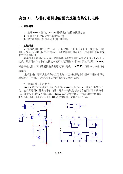
实验3.2 与非门逻辑功能测试及组成其它门电路一、实验目的:1.熟悉THD-1型(或Dais-2B型)数电实验箱的使用方法。
2. 了解基本门电路逻辑功能测试方法。
3.学会用与非门组成其它逻辑门的方法。
二、实验准备:1. 集成逻辑门有许多种,如:与门、或门、非门、与非门、或非门、与或非门、异或门、OC门、TS门等等。
但其中与非门用途最广,用与非门可以组成其它许多逻辑门。
要实现其它逻辑门的功能,只要将该门的逻辑函数表达式化成与非-与非表达式,然后用多个与非门连接起来就可以达到目的。
例如,要实现或门Y=A+B,A ,可用三个与非门连根据摩根定律,或门的逻辑函数表达式可以写成:Y=B接实现。
集成逻辑门还可以组成许多应用电路,比如利用与非门组成时钟脉冲源电路就是其中一例,它电路简单、频率范围宽、频率稳定。
2. 集成电路与非门简介:74LS00是“TTL系列”中的与非门,CD4011是“CMOS系列”中的与非门。
它们都是四-2输入与非门电路,即在一块集成电路内含有四个独立的与非门。
每个与非门有2个输入端。
74LS00芯片逻辑框图、符号及引脚排列如图与非门的逻辑功能是:当输入端中有一个或一个以上是低电平时,输出端为高电平;只有当输入端全部为高电平时,输出才是低电平(即有“0”得“1”,全“1”得“0”)。
其逻辑函数表达式为:B=。
Y⋅ATTL电路对电源电压要求比较严,电源电压Vcc只允许在+5V±10%的范围内工作,超过5.5V将损坏器件;低于4.5V器件的逻辑功能将不正常。
CMOS集成电路是将N沟道MOS晶体管和P沟道MOS晶体管同时用于一个集成电路中,成为组合两种沟道MOS管性能的更优良的集成电路。
CMOS电路的主要优点是:(1). 功耗低,其静态工作电流在10-9A数量级,是目前所有数字集成电路中最低的,而TTL器件的功耗则大得多。
(2).高输入阻抗,通常大于1010Ω,远高于TTL器件的输入阻抗。


数字电路实验M u l t i s i m仿真HEN system office room 【HEN16H-HENS2AHENS8Q8-HENH1688】实验一逻辑门电路一、与非门逻辑功能的测试74LS20(双四输入与非门)仿真结果二、门)三、与或非门逻辑功能的测试四、现路;一、分析半加器的逻辑功能二.74LS138接成四线-十六线译码器 00000001011110001111(2)用一片74LS153接成两位四选一数据选择器; (3)用一片74LS153一片74LS00和接成一位全加器(1)设计一个有A 、B 、C 三位代码输入的密码锁(假设密码是011),当输入密码正确时,锁被打开(Y 1=1),如果密码不符,电路发出报警信号(Y 2=1)。
以上四个小设计任做一个,多做不限。
还可以用门电路搭建实验三 触发器及触发器之间的转换1. D 触发器逻辑功能的测试(上升沿)2. JK 触发器功能测试(下降沿)Q=0Q=0略3. 思考题:(1)(2)(3)略实验四寄存器与计数器1.右移寄存器(74ls74 为上升沿有效)位异步二进制加法,减法计数器(74LS112 下降沿有效)也可以不加数码显示管3.设计性试验(1)74LS160设计7进制计数器(74LS160 是上升沿有效,且异步清零,同步置数)若采用异步清零:若采用同步置数:(2)74LS160设计7进制计数器略(3)24进制83进制注意:用74LS160与74LS197、74LS191是完全不一样的实验五 555定时器及其应用1.施密特触发器输入电压从零开始增加:输入电压从5V开始减小:2.单稳态触发器3.多谢振荡。
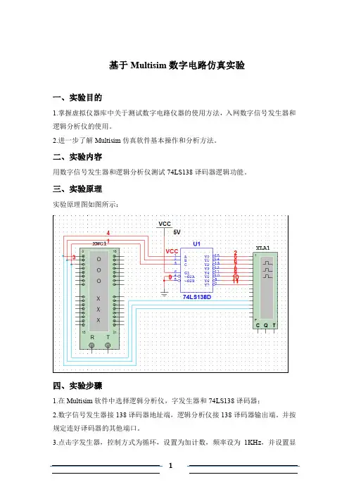
基于Multisim数字电路仿真实验一、实验目的1.掌握虚拟仪器库中关于测试数字电路仪器的使用方法,入网数字信号发生器和逻辑分析仪的使用。
2.进一步了解Multisim仿真软件基本操作和分析方法。
二、实验内容用数字信号发生器和逻辑分析仪测试74LS138译码器逻辑功能。
三、实验原理实验原理图如图所示:四、实验步骤1.在Multisim软件中选择逻辑分析仪,字发生器和74LS138译码器;2.数字信号发生器接138译码器地址端,逻辑分析仪接138译码器输出端。
并按规定连好译码器的其他端口。
3.点击字发生器,控制方式为循环,设置为加计数,频率设为1KHz,并设置显示为二进制;点击逻辑分析仪设置频率为1KHz。
相关设置如下图五、实验数据及结果逻辑分析仪显示图下图实验结果分析:由逻辑分析仪可以看到在同一个时序74LS138译码器的八个输出端口只有一个输出为低电平,其余为高电平.结合字发生器的输入,可知.在译码器的G1=1,G2A=0,G2B=0的情况下,输出与输入的关系如下表所示当G1=1,G2A=0,G2B=0中任何一个输入不满足时,八个输出都为1六、实验总结通过本次实验,对Multisim的基本操作方法有了一个简单的了解。
同时分析了38译码器的功能,结果与我们在数字电路中学到的结论完全一致。
实验二基于Multisim的仪器放大器设计一、实验目的1.掌握仪器放大器的实际方法;2.理解仪器放大器对共模信号的抑制能力;3.熟悉仪器放大器的调试方法;4.掌握虚拟仪器库中关于测试模拟电路仪器的使用方法,如示波器、毫伏表、信号发生器等虚拟仪器的使用方法。
二、实验内容1.采用运算放大器设计并构建仪器放大器,具体指标为:(1)输入信号Ui=2mv时,要求输出电压信号Uo=0.4V,Avd=200,f=1KHz;(2)输入阻抗要求Ri》1MΩ2.用虚拟仪器库中关于测试模拟电路仪器,按设计指标进行调试;3.测量所构建的测量放大器的共模抑制比(选做)4.记录实验数据进行整理分析。

(完整)数字逻辑实验指导书(multisim)编辑整理:尊敬的读者朋友们:这里是精品文档编辑中心,本文档内容是由我和我的同事精心编辑整理后发布的,发布之前我们对文中内容进行仔细校对,但是难免会有疏漏的地方,但是任然希望((完整)数字逻辑实验指导书(multisim))的内容能够给您的工作和学习带来便利。
同时也真诚的希望收到您的建议和反馈,这将是我们进步的源泉,前进的动力。
本文可编辑可修改,如果觉得对您有帮助请收藏以便随时查阅,最后祝您生活愉快业绩进步,以下为(完整)数字逻辑实验指导书(multisim)的全部内容。
实验一集成电路的逻辑功能测试一、实验目的1、掌握Multisim软件的使用方法。
2、掌握集成逻辑门的逻辑功能。
3、掌握集成与非门的测试方法。
二、实验原理TTL集成电路的输入端和输出端均为三极管结构,所以称作三极管、三极管逻辑电路(Transistor -Transistor Logic )简称TTL电路。
54 系列的TTL电路和74 系列的TTL电路具有完全相同的电路结构和电气性能参数。
所不同的是54 系列比74 系列的工作温度范围更宽,电源允许的范围也更大。
74 系列的工作环境温度规定为0—700C,电源电压工作范围为5V±5%V,而54 系列工作环境温度规定为-55—±1250C,电源电压工作范围为5V±10%V.54H 与74H,54S 与74S 以及54LS 与74LS 系列的区别也仅在于工作环境温度与电源电压工作范围不同,就像54 系列和74 系列的区别那样。
在不同系列的TTL 器件中,只要器件型号的后几位数码一样,则它们的逻辑功能、外形尺寸、引脚排列就完全相同。
TTL 集成电路由于工作速度高、输出幅度较大、种类多、不易损坏而使用较广,特别对我们进行实验论证,选用TTL 电路比较合适。
因此,本实训教材大多采用74LS(或74)系列TTL 集成电路,它的电源电压工作范围为5V±5%V,逻辑高电平为“1”时≥2。
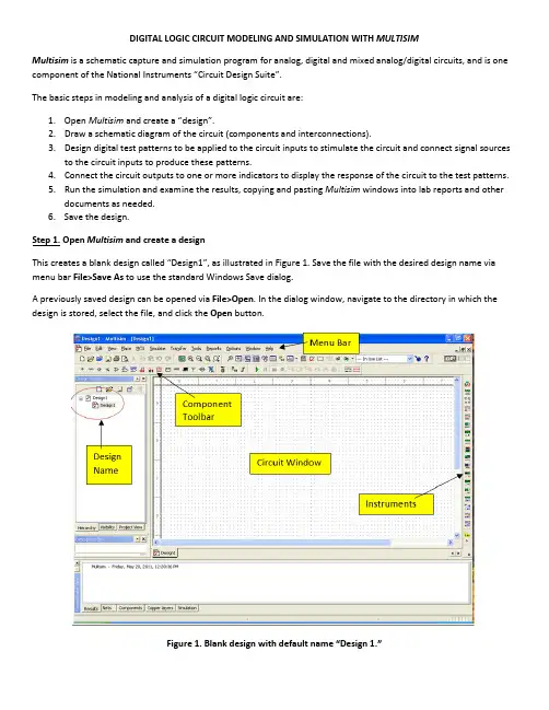
DIGITAL LOGIC CIRCUIT MODELING AND SIMULATION WITH MULTISIMMultisim is a schematic capture and simulation program for analog, digital and mixed analog/digital circuits, and is one component of the National Instruments “Circuit Design Suite”.The basic steps in modeling and analysis of a digital logic circuit are:1.Open Multisim and create a “design”.2.Draw a schematic diagram of the circuit (components and interconnections).3.Design digital test patterns to be applied to the circuit inputs to stimulate the circuit and connect signal sourcesto the circuit inputs to produce these patterns.4.Connect the circuit outputs to one or more indicators to display the response of the circuit to the test patterns.5.Run the simulation and examine the results, copying and pasting Multisim windows into lab reports and otherdocuments as needed.6.Save the design.Step 1. Open Multisim and create a designThis creates a blank design called “Design1”, as illustrated in Figure 1. Save the file with the desired design name via menu bar File>Save As to use the standard Windows Save dialog.A previously saved design can be opened via File>Open. In the dialog window, navigate to the directory in which the design is stored, select the file, and click the Open button.Figure 1. Blank design with default name “Design 1.”Step 2. Draw a schematic diagram of the circuitPlace ComponentsA schematic diagram comprises one or more circuit components, interconnected by wires. Optionally, signal “sources” may be connected to the circuit inputs, and “indicators” to the circuit outputs. Each component is selected from the Multisim library and placed on the drawing sheet in the Circuit Window (also called the Workspace). The Multisim library is organized into “groups” of related components (Transistors, Diodes, Misc Digital, TTL, etc.). Each group comprises one or more “families”, within which the components are implemented with a common technology. For designing and simulating digital logic circuits in this course, “Misc Digital” (TIL family only) is used.The “Misc Digital” group has three families of components, of which family “TIL” contains models of generic logic gates, flip-flops, and modular functions. These components are technology-independent, which means that they have only nominal circuit delays and power dissipation, unrelated to any particular technology. Generic components can be used to test the basic functionality of a design, whereas realistic timing information requires the use of technology-specific part models, such as those in the TTL group.To place a component on the drawing sheet, select it via the Component Browser, which is opened via the component toolbar or the menu bar. From the menu bar, select Place>Component to open the Component Browser window, illustrated in Figure 2. You can also open this window by clicking on the Misc Digital icon in the component toolbar. On the left side of the window, select “Master Database”, group “Misc Digital”, and family “TIL”. The component panel in the center lists all components in the selected family. Scroll down to and click on the desired gate (NAND2 Figure 3); its symbol and description are displayed on the right side of the window. Then click the OK button. The selected gate will be shown on the drawing sheet next to the cursor; move the cursor to position the gate at the desired location, and then click to fix the position of the component. The component can later be moved to a different location, deleted, rotated, etc. by right clicking on the component and selecting the desired action. You may also select these operations via the menu bar Edit menu.Figure 2. Component Browser: Misc Digital TIL family NAND2 gate component selected.Figure 3. A third NAND2 gate is about to be placed on the drawing sheet.Figure 4 shows the schematic diagram with four placed components. Note that each placed gate has a “designator” (U2, U3, U4, U5), which can be used when referring to that gate. You can change a designator by right clicking on the component, selecting Properties, and entering the desired name on the Label tab.Figure 4. Schematic diagram with all placed components.Drawing WiresWires are drawn between component pins to interconnect them. Moving the cursor over a component pin changes the pointer to a crosshair, at which time you may click to initiate a wire from that pin. This causes a wire to appear, connected to the pin and the cursor. Move the cursor to the corresponding pin of the second component (the wire follows the cursor) and click to terminate the wire on that pin. If you do not like the path selected for the wire, you may click at a point on the drawing sheet to fix the wire to that point and then you can move the cursor to continue the wire from that point. You may also initiate or terminate a wire by clicking in the middle of a wire segment, creating a “junction” at that point. This is necessary when a wire is to be fanned out to more than one component input. A partially-wired circuit, including one junction point, is illustrated in Figure 5.Figure 5. Partially wired circuit, with one junction point.Step 3. Generating test input patterns.To drive circuit simulations, Multisim provides several types of “sources” and “instruments” to generate and apply patterns of logic values to digital circuit inputs. Sources are placed on the schematic sheet and connected to circuit inputs in the same way as circuit components, selecting them from the “Digital_Sources” family of the “Sources” group in the component browser. Note that there is a Place Source shortcut icon in the tool bar.There are three basic digital sources:1.DIGITAL_CONSTANT – this is a box with a constant logic 1 or 0 output, and would be used where the logic valueis not to be changed during simulation. To change the output value, right click on the box, select Properties, select the desired value on the Value tab, and click the OK button.2.INTERACTIVE_DIGITAL_CONSTANT – this is a clickable box that can be connected to a circuit input. Clicking onthe box toggles its output between 0 and 1. This can be used to interactively change a circuit input duringsimulation.3.DIGITAL_CLOCK – this is a box that produces a repeating pulse train (square waveform), oscillating between 0and 1 at a specified frequency. To set the frequency and duty cycle, right click on the box, select Properties,select the desired frequency and duty cycle value on the Value tab, and click the OK button.Figure 6 shows the circuit of Figure 5 with an INTERACTIVE_DIGITAL_CONSTANT connected to each input. Note that the initial state of each is logic 0. Since this circuit has only three inputs, all 8 input patterns can be produced (to generate a truth table for the circuit) by manually toggling the inputs.Figure 6. INTERACTIVE_DIGITAL_CONSTANT sources connected to circuit inputs.Step 4. Connect circuit outputs to indicatorsTo facilitate studying the digital circuit output(s), Multisim provides a variety of “indicators”. For digital simulation, the most useful are digital “probes”, hex displays, and the Logic Analyzer instrument. A probe, illustrated in Figure 7, displays a single digital value as ON or OFF (the probe is “illuminated” indicating an ON condition). The PROBE family of the Indicators group includes a generic PROBE_DIG and several PROBE_DIG_color indicators (color = BLUE, GREEN, ORANGE, RED, YELLOW). The probe in Figure 7 is PROBE_DIG_BLUE. This circuit can be verified by manually changing the three INTERACTIVE_DIGITAL_CONSTANT inputs to each of the 8 possible combinations, and recording the probe value for each combination to create a truth table.Figure 7. DIGITAL_PROBE_BLUE connected to circuit output.Step 5. Run the simulationA simulation is initiated by pressing the Run (green arrow) button in the toolbar or via the menu bar via Simulate>Run. You may simulate the circuit by clicking on the keys to change the input values and observe the output changes through the LED indicator.You may capture any window and paste it into a Word or other document for generating reports. An individual window is captured by pressing the ALT and Print Screen keys concurrently. You may then “paste” the captured window into a document via the editing features of that document. To capture a circuit diagram in the main window, the simplest method is via the menu bar Tools>Capture Screen Area. This produces a rectangle whose corners can be stretched to include the screen area to be captured; the “copy” icon on the top left corner is pressed to copy the area, which may then be pasted into a document.Step 6. Save the design and close MultisimThe simplest way to save a design is to click the Save icon in the Design Toolbar on the left side of the window, directly above the design name. Alternatively, you may use the standard menu bar File>Save.Multisim is exited as any other Windows program.-This document is a modified and short version of /department/ee/elec2210/.Appendix: Creating subcircuits and hierarchical blocks (from NI Multisim manual)Complete the following steps to place a new subcircuit:1. Select Place»New subcircuit. The Subcircuit Name dialog box appears.2. Enter the name you wish to use for the subcircuit, for example, “PowerSupply” andclick OK. Your cursor changes to a “ghost” image of the subcircuit indicating that thesubcircuit is ready to be placed.3. Click in the desired location to place the subcircuit.4. Double-click on the new subcircuit and select Open subsheet from the Label tab ofthe Hierarchical Block/Subcircuit dialog box that displays. An empty design sheetappears.5. Place and wire components as desired in the new subcircuit.6. Select Place»Connectors»Hierarchical connector, and place and wire the connector asdesired. Repeat for all required hierarchical connectors.When you attach a hierarchical connector to a wire, the net name for the wire that you connect it to does not change if it has a Preferred net name (user-assigned via the NetProperties dialog box). If the net name on the wire is auto-named, it changes to match theconnector.7. Select the sheet that contains the subcircuit from the Hierarchy tab of the DesignToolbox.OrSelect View»Parent sheet.This command moves you up to the next sheet in the hierarchy. If you have multiple nested circuits and are viewing, for example, a subcircuit within a subcircuit, you will notmove to the top of the hierarchy.The symbol for the subcircuit that appears includes pins for the number of connectors thatyou added.8. Wire the hierarchical connectors into the main circuit.Complete the following steps to place another instance of the same subcircuit:1. Select the desired subcircuit and select Edit»Copy.2. Select Edit»Paste to place a copy of the subcircuit on the workspace.。

第16卷第6期20cr7年11月平顶山工学院学报J01lrIlal0fH喇ngs}laIlh曲mteof‰llIl蛔V01.16No.6Nov.200r7文章编号:167l二9662(2007)06—0cr77—03基于Multisim8的数字电路课程设计与仿真杨庆(湖北民族学院电气工程系,湖北恩施445000)摘要:应用Mu城silI・8进行数字电路课程设计虚拟仿真实验可以有效地克服课程设计实验难于保证的问题。
文章介绍了M111石sim8软件仿真功能的特点,并通过实例说明了用Mu】6sim8软件进行数字电路课程设计、仿真分析的具体方法。
关键词:Ml越曲8;数字电路;课程设计;仿真中图法分类号:删,G434,TP39文献标识码:AO引言在电子技术高速发展的今天,采用软件仿真的方法,在计算机上虚拟出一个测试仪器先进、元器件品种齐全的电子工作台,一方面克服了实验室的条件限制,避免了使用中仪器损坏等不利因素,另一方面又能以验证型、测试型、设计型、纠错型和创新型等不同形式的针对性训练,培养学生的分析、应用和创新能力。
同时,通过计算机完成电路的功能设计、性能分析、时序测试以及印刷线路板的自动布线,使学生了解使用EDA技术进行产品设计的基本过程。
与传统的实验方式相比较,采用计算机虚拟技术进行电子线路的分析和设计,突出了实验教学以学生为中心的开放模式,不仅实验的效率得到提高,而且在训练学生掌握正确的测量方法和熟练使用仪器的能力、电路的综合分析能力和创新能力上都有比较明显的改善和提高…。
1M出sim8介绍M11l颤m8是加拿大Inten蜘vehIlage7№h谳09ies公司继M出silIl2001、M出siIIl7之后,于2004年推出的M11ldsim最新版本,是该公司电子电路仿真软件EwB(E‰ⅡoIIicswDdkbench,虚拟电子工作台)的升级版。
目前,EⅣB包含电路仿真设计的模块Ml,16sjm、PCB设计软件In曲∞rd、布线引擎IⅡ右mllte和通信电路分析与设计模块con哪iIn4个部分,能完成从电路仿真设计到电路板图生成的全过程。