资深项目专家教你快速搞定硬件产品开发刘涛(发烧友直播20181227)
- 格式:pptx
- 大小:1.24 MB
- 文档页数:23


楼宇自控系统目录目录 (2)第一部分工程概略与系统解决方案说明 (4)1-1工程概略 (4)1-2楼宇自控系统简介 (4)1-3设计依照 (5)第二部分用户需求剖析 (6)2-1技术层面 (6)2-2建筑运转管理层面 (7)2-3公司营运层面 (7)第三部分系统设计 - 系统架构设计及设施选型说明 (9)3-1系统架构设计说明 (9)3-1.1系统架构的开放性和可集成程度要求 (9)3-1.2鉴于 TCP/IP 网络架构 (10)3-1.3鉴于 WEB 和 B/S 的网络架构 (11)3-1.4采纳功能强盛、能够进行现场集成的网络控制器 (12)3-2产品选型说明 (13)3-3 Honeywell WEBs系统架构 (16)3-4设施配置 (22)第四部分系统设计 - 系统功能控制方案说明 (24)4-1系统控制方案设计原则 (24)4-2节能控制方案 (25)4-2.1.提升室内温度控制精度 (25)4-2.2.机电设施最正确启停控制 (26)4-2.3.空调水系统均衡与变流量管理 (26)4-3冷热源系统监控 (27)4-4空调通风系统 (28)4-5送排风机组 (30)4-6给排水系统 (30)4-7照明系统 (30)4-8电梯系统 (31)第五部分 Honeywell WEBs控制设施介绍 (32)5-1 WEBSTATION-AX TM网络服务器 (32)5-2 WEBPro-AX编程工具 (33)5-3 WEB-700网络控制器 (34)5-4 现场层 DDC 控制器 : (35)第六部分系统实行 (39)6-1网络环境建设 (39)6-2系统编程 (39)6-3系统试运转和查收 (39)6-4项目任务分解方案 (40)第七部分附录 (41)7-1系统点表 (41)7-2系统设施清单 (41)7-3系统图 (41)7-4设施原理图 (41)第一部分工程概略与系统解决方案说明1-1 工程概略*****************************1-2 楼宇自控系统简介楼宇自控系统( BAS)是建筑技术、自动控制技术与计算机网络技术相联合的产物,使大楼拥有智能建筑的特征。


,dSPACE*** 基于Matlab/Simulink平台***实时快速原型及硬件在回路仿真的一体化解决途径恒润科技有限公司2004年6月目录1概述 (1)2dSPACE—实时快速原型及硬件在回路仿真的一体化解决途径 (1)2.1RCP(Rapid Control Prototyping)—快速控制原型 (1)2.2HILS(Hardware-in-the-Loop Simulation)—硬件在回路仿真 (1)2.3用dSPACE进行控制系统开发 (1)2.4建立用户dSPACE系统 (1)3dSPACE体系结构 (1)3.1dSPACE软件 (1)3.1.1代码生成及下载软件(Implementation Software) (1)3.1.1.1代码的生成过程 (1)3.1.1.2MATLAB/Simulink-现代控制设计平台 (1)3.1.1.3RTI(Real-Time Interface)-从方框图自动生成代码并下载 (1)3.1.1.4PPC编译器 (1)3.1.2实验软件(Experiment Software) (1)3.1.2.1ControlDesk综合实验环境 (1)3.1.2.2MLIB和MTRACE—实现自动试验及参数调整 (1)3.1.2.3MotionDesk—实时动画 (1)3.1.2.4CLIB---PC与实时处理器通讯 (1)3.1.2.5AutoMationDesk-自动化测试工具 (1)3.1.3TargetLink-产品级代码的生成 (1)3.2dSPACE硬件 (1)3.2.1智能化的单板系统 (1)3.2.1.1DS1103 PPC 控制器板 (1)3.2.1.2DS1104 PPC 控制器板 (1)3.2.2标准组件系统 (1)3.2.2.1处理器板(Processor Boards) (1)3.2.2.1.1处理器板概述(总线和中断) (1)3.2.2.1.2DS1005 PPC板-处理器POWER PC750FX,800MHz (1)3.2.2.1.3DS1006 PPC板-处理器X86处理器,2.2GHz (1)3.2.2.2I/O板 (1)3.2.2.2.1简单A/D和D/A转换 (1)3.2.2.2.2Multi-I/O (1)北京恒润科技有限公司 13.2.2.2.3增量编码器接口 (1)3.2.2.2.4定时及数字I/O (1)3.2.2.2.5复杂模拟信号及阻型传感器 (1)3.2.2.2.6其它I/O (1)3.2.2.2.7DS2211 HIL I/O板 (1)3.2.2.3附件(Accessories) (1)3.2.2.3.1大系统扩展盒PX10/PX20 (1)3.2.2.3.2接插键指示灯面板 (1)3.2.2.3.3DS830连接缓冲器板-连接远距离系统 (1)3.2.3汽车内置系统 (1)3.2.3.1AutoBox-汽车内置试验扩展箱 (1)3.2.3.2MicroAutoBox-车辆快速测试控制原型系统的最佳选择 (1)4应用实例 (1)4.1机器人新型控制原理测试--用μ-综合与分析法控制机械手 (1)4.2驱动方面的应用-验证ASIC控制器原理 (1)4.3机械工程方面的应用—Achenbach Buschhüten 平面度控制 (1)4.4航空航天方面的应用—Simona开发飞行仿真器 (1)4.5汽车的硬件在回路仿真—ABS控制器测试试验台 (1)4.6电力电子方面的应用-机车驱动系统硬件在回路仿真 (1)4.7ECU开发应用-菲亚特公司开发ERG控制器 (1)4.8DaimlerChrysler开发主动悬架 (1)4.9Delphi利用Targetlink进行电控产品开发 (1)4.10Audi公司动力传动系统HIL仿真测试 (1)4.11DS2302、DS4002的应用实例 (1)附录1—I/O板技术特性 (1)附录2—dSPACE对计算机软件及硬件的要求 (1)北京恒润科技有限公司 21概述在当今社会,市场对产品的需求呈现多样性、快速性的趋势,这就使企业的新品开发面临着多样性需求与快速开发之间的矛盾;对控制系统鲁棒性及可靠性的要求也日益增加;并行工程(即:设计、实现、测试和生产准备同时进行)被提上了日程。

UG0872User Guide PolarFire MPF300T FPGA Video KitJune 20191Revision History (1)1.1Revision 1.0 (1)2Introduction (2)2.1Kit Contents (2)2.2Block Diagram (2)2.3Board Overview (3)3Hardware Settings (6)3.1Jumper Settings (6)3.2LEDs (6)3.3Power Sources (7)4Board Components and Operations (9)4.1Memory Interface (9)4.2SPI Serial Flash (9)4.3HDMI1.4 Interface (10)4.4MIPI-RX Connector (CSI-2 Application) (10)4.5MIPI-TX Connector (DSI Application) (11)4.6MIPI-TX Connector (CSI-2 Application) (11)4.7MIPI-TX and RX PCB Loopback (12)4.8Transceivers (12)4.8.1XCVR0 Block (12)4.8.2XCVR1 and XCVR3 Blocks (13)4.8.3XCVR2 Block (14)4.8.4XCVR Reference Clock (15)4.9Programming (15)4.9.1FTDI and JTAG Header Scheme (15)4.1050 MHz Oscillator (16)4.11Device Reset (17)4.12User Reset (17)4.13User Interface (17)4.13.1User LEDs (18)4.13.2Push-Button Switches (18)4.13.3Slide Switches (DPDT) (19)4.13.4DIP Switches (SPST) (19)4.13.5FMC HPC Connector (J14) (20)4.14Board Components Placement (20)The revision history describes the changes that were implemented in the document. The changes arelisted by revision, starting with the most current publication.1.1Revision 1.0Revision 1.0 was the first publication of this documentThe Microsemi PolarFire® FPGA Video Kit (POLARFIRE VIDEO KIT), which is RoHS-compliant, enables youMPF300T-1FCG1152Eto evaluate the PolarFire FPGA for the following interfaces:MIPI CSI-2 RX interfaceHDMI2.0HDMI1.4DDR4 memoryFMC HPC with 8 Transceiver lanesUART Interface to the FTDI deviceSPI Interface to the SPI Flash device2.1Kit ContentsThe following table lists the contents of the PolarFire Video Kit.Table 1 • Kit ContentsItem QuantityDual Camera Sensor Module1PolarFire Video Board featuring the device with 300K logic elementsMPF300T-1FCG1152E 112 V, 5 A AC power adapter and cord1USB 2.0 A-male to mini-B cable programming1Quickstart card1Free one-year Libero Gold software license12.2Block DiagramThe following figure shows the block diagram of the video kit.Figure 1 • Block Diagram2.3Board OverviewThe following figure shows a labeled image of the video board highlighting its components.Figure 2 • Board CalloutThe following table lists the components of the video board.Table 2 • Board ComponentsComponent Label onBoardDescriptionFeatured DevicePolarFire FPGA FPGAMPF300T-1FCG1152EPower Supply12 V power supply J20The board is powered by a 12 V power source using an external +12 V/5 A DC jack ON/OFF switch SW4Power ON/OFF switch from +12 V external DC jackClocksOn-board 50 MHzclock oscillatorX350 MHz clock oscillator with single-ended outputXCVR reference clock Y5148.5 MHz oscillator (differential LVDS output) that provides reference clock(REFCLK) via PolarFire device pins AF29 and AF30. These pins are connected to theXCVRClock Synthesizer U15CDCEL913PWR Clock Synthesizer for HDMI1.4 clocks and programmable throughthe I2CFPGA Programming and DebuggingFT4232H U70USB-to-quad serial ports in various configurationsJTAG programming header J18This header is used to program and debug the PolarFire device using FlashPro4 or FlashPro5. In the FlashPro software, the appropriate programmer (FlashPro4orFlashPro5) must be selected.SPI flash U30One 1 Gb SPI Flash from Micron MT25QL01GBBB8ESF-0SIT (P/N) connected to SPIpins on bank 3 of the PolarFire deviceMemory ChipsDDR4 Memory U1,U2,U3 andU4Four 4 Gb (MT40A256M16GE-083E:B) chips are connected in Fly-by topology with a 64-bit data bus for storing data bitsFMC HPC connector J14FMC connector with eight XCVR lanes and 13 Differential pairs HPC[HA0:12] and LPC[0:33])Video InterfacesCSI-2 RX connector J5MIPI data and clock signals are received from Camera sensor boardDSI TX connector J26MIPI data and clock signals are transmitted to Display daughter board through theconnectorCS-2 TX connector J4MIPI data and clock signals are transmitted to Display daughter board through theconnectorGeneral Purpose I/OSwitches SW1 andSW2Push-button switches for user-interface debugging applicationsDIP Switches SW6Four DIP switches for testingLight-emitting diodes (LEDs)Four active-high LEDs connected to some of the user I/Os for debugging, and twelve active high LEDs used for indicating power supplyComponent Label onBoardUSER Reset switch SW3Push-button system reset for the PolarFire device Users must program this HSIO forPolarFire logic reset functionDevice reset SW5Device reset3Hardware SettingsThis section provides information about jumper settings, switches, LEDs, and DIP switches on thePolarFire video board.3.1Jumper SettingsConnect the jumpers according to the settings specified in the following table.Table 3 • Jumper SettingsJumper Description Pin(s)DefaultJ15SPI Slave and Master mode selection. By DefaultSPI master1-2Closed J19XCVR_VREF is connected to GND1-2ClosedJ28Close pin 1-2 to program through the FTDI Openpin 1-2 to program the external Flash pro51-2ClosedJ24Jumper to select the PolarFire VDDAUX4 for Bank4 voltage Close pin2-4 for 3V3Close pin2-4 for 2V5ClosedOpenJ25Jumper to select the PolarFire VCCIO voltage (VCCIO_HPC_VADJ)Close pin 1 and 2 for 3.3 VClose pin 3 and 4 for 2.5 VClose pin 5 and 6 for 1.8 VClose pin 7 and 8 for 1.5 VClose pin 9 and 10 for 1.2 VOpenOpenClosedOpenOpenJ36Jumper to select the SW3 input or theENABLE_FT4 232 signal from the FT4232H chip Close pin 1 and 2 for manual power switchingusing SW3Close pin 2 and 3 for remote power switchingusing the GPIO capability of the FT4232 chipCloseOpen3.2LEDsThe following table lists the power supply LEDs.Table 4 • LEDsLED DescriptionDS14-Green12 V voltage railDS20-Green 5 V voltage railDS21-Green 3.3V voltage railDS5-Green 1.0V voltage railDS4-Green 1.8V voltage railDS3-Green VDD25 Voltage railDS2-Green VDDAUX2_5 Voltage railLED DescriptionDS9-Green VDDA(1V05) Voltage railDS8-Green VDDAUX4 Voltage railDS7-Green 1.2V voltage railDS6-Green VCCIO_HPC_VADJ voltage railDS12-Green 1.8V HDMI1V4 voltage railDS13-Green0.6V VTT voltage rail3.3Power SourcesThe PolarFire video board uses Microchip power supply devices. For more information about thesepower supply devices, see: https:///design-centers/power-management/dc-dc-converters-regulators.The following table lists the key power supplies required for normal operation of the PolarFire videoboard.Table 5 • Voltage Rails in PolarFire Video BoardPolarFire Bank I/O Rail VoltageBank 01P2V 1.2VBank 11P8V 1.8VBank 21P2V_B2 1.2VBank 3VDD25 2.5VBank 4VCCIO_HPC_VADJ 1.8VBank 5VDD25 2.5VBank 61P8V_HDMI1V4 1.8VBank 71P2V 1.2VThe following figure shows the power supply scheme used in the PolarFire video board.Figure 3 • Power Supply SchemeThe following table lists the suggested Microchip power regulators for PolarFire FPGA voltage rails.Table 6 • Power RegulatorsVoltage Rail Part Number Description Current5V MIC24055YJL-TR IC REG BUCK ADJ 12A SYNC 28QFN12A1V MIC24055YJL-TR IC REG BUCK ADJ 12A SYNC 28QFN12A1V2MIC24046YFL-TR IC REG BUCK PROG 5A SYNC 20VQFN5AVDDAUX2&5MIC23303YML-T5IC REG BUCK ADJ 3A SYNC 12DFN3AVDDAUX4MIC23303YML-T5IC REG BUCK ADJ 3A SYNC 12DFN3AVCCIO_HPC_VADJ MIC24046YFL-TR IC REG BUCK PROG 5A SYNC 20VQFN5AVREF,VTT MIC5166YML-TR IC PWR SUP 3A HS DDR TERM 10MLF3AHDMI1.4MCP1726T-ADJE/MF IC REG LINEAR POS ADJ 1A 8DFN1AVDD25MIC69502WR IC REG LINEAR POS ADJ 5A SPAK-75A3V3MIC69502WR IC REG LINEAR POS ADJ 5A SPAK-75AVDD18MIC69502WR IC REG LINEAR POS ADJ 5A SPAK-75A1V05MIC69502WR IC REG LINEAR POS ADJ 5A SPAK-75ANote: These regulators are not pin compatible with the existing video kit schematics. Use these regulators for new board.4Board Components and OperationsThis section describes the key components of the PolarFire Video board and important boardoperations.4.1Memory InterfaceThe following figure shows the memory interface scheme.Figure 4 • Memory InterfaceAs shown in the preceding figure, Four 4 Gb DDR4 SDRAM chips are used as flexible volatile memory foruser applications. The DDR4 interface is implemented in the HSIO Bank 0 and Bank 7.The DDR4 SDRAM specifications are as follows:MT40A256M16GE-083E:BQuantity: Four chips are connected in Fly-by topologyDensity: 16 GbData rate: DDR4 64-bit at 166 MHz clock rateThe PolarFire video board design uses the DDR4 and POD12 standards for the DDR4 interface. Thedefault board assembly for the DDR4 standard uses RC terminations.4.2SPI Serial FlashThe following figure shows the SPI Flash and its interface with the PolarFire device.The SPI flash specifications for the PolarFire device are:Density: 1 GbVoltage: 2.7 V to 3.6 V (MT25QL01GBBB8ESF-0SIT)Frequency: 90 MHz Quantity = 1SPI mode support: Modes 0 and 34.3HDMI1.4 InterfaceOne HDMI1.4 Transmitter is connected to the PolarFire device to support the HDMI1.4 standard as shown in the following figure.Figure 6 • HDMI1.4 InterfaceThe HDMI interface is implemented in Bank6.The HDMI1.4 transmitter specifications for the PolarFire device are:Part Number of the HDMI Transmitter: ADV7511KSTZ Operating frequency: up to 225 MHz4.4MIPI-RX Connector (CSI-2 Application)The video board supports a dual Camera image sensor daughter card that can be connected using the CSI-2 RX interface (J5) for CSI-2 RX applications. The daughter card includes two IMX334 cameras. Each image sensor supports a four-lane MIPI interface. The daughter card is connected to the video board via the board to board connector as shown in the following figure The MIPI output signals . (see page )are connected to Bank 2.The image sensor supports maximum 1782 Mbps.4.5MIPI-TX Connector (DSI Application)The video board supports the MIPI transmitter X4 lanes and clock for DSI application, as shown in thefollowing figure. MIPI TX signals are interfaced to the LCD display. An adaptor board for the LCD displaycan be connected through the J26 connector on the video board. This adaptor board contains the LCDmating connector and the auxiliary circuit required for the display. For more information, see the videoboard schematics.Figure 8 • MIPI-TX Connection (DSI Application)4.6MIPI-TX Connector (CSI-2 Application)The video board supports the MIPI X4 lanes and clock for the CSI-2 transmitter application, as shown inthe following figure. For testing, the video board can be can be interfaced with Nvidia’s Jetson TX1\TX2development board using a mating connector cable.Figure 9 • MIPI-TX Connection (CSI-2 Application)`4.7MIPI-TX and RX PCB LoopbackThe video board supports the on-board PCB trace loopback of MIPI X4 lanes and clock, as shown in thefollowing figure.Figure 10 • MIPI-TX and RX Loopback4.8TransceiversMPF300T-1FCG1152EThe PolarFire FPGA device has 4 XCVR blocks and each block contains 4transceiver lanes. These lanes can be accessed through the HDMI2.0 and FMC connectors on the board.The following sections describe these blocks and the lanes used.4.8.1XCVR0 BlockLanes 0, 1, and 2 of the XCVR0 block are looped back, as shown in the following figure .Figure 11 • XCVR0 Interface4.8.2XCVR1 and XCVR3 BlocksXCVR1 and XCVR3 blocks have four lanes each. These lanes are connected to the FMC HPC connectorand the signals are routed on the PCB as follows:Lanes 0 to 7 are directly routed to the FMC HPCTX pad > trace > via (to bottom layer) > trace > FMC HPC connector padRX pad > trace > via (to Top layer) > trace > PolarFire device padThe XCVR1 and XCVR3 reference clock is routed directly from the HPC connector to the PolarFire device.The following figure shows the XCVR1 and XCVR3 and their interfaces.Figure 12 • XCVR1 and XCVR3 Interface4.8.3XCVR2 BlockThe lanes of the XCVR2 block are connected to HDMI2.0 TX and RX chips via the line drivers chips, asshown in the following figure. This interface can operate up to 6 Gbps.Figure 13 • XCVR2 Interface4.8.4XCVR Reference ClockThe following figure shows the clock sources for XCVR blocks.Figure 14 • XCVR Reference ClocksXCVR 1A, 3A reference clocks are sources from FMC HPC connector(J14).XCVR 2B reference clock is sourced from the on-board 148.5 MHzXCVR 2A reference clock is sourced from the on-board HMDI2.0 TX4.9ProgrammingThe PolarFire device is programmed using the on-board FlashPro5 programmer or through the JTAGvideo board schematicsHeader. For more information about programming, see the .The following section describes the FTDI and JTAG Header programming schemes used on the board.4.9.1FTDI and JTAG Header SchemeThe PolarFire device can be programmed using the on-board JTAG Header or FTDI. By default, the FTDIprogramming mode is enabled. The programming mode can be changed based on the Jumper settings.Table 3For more information, see .The following figure shows how the JTAG Header interfaces with the PolarFire Device.Figure 15 • JTAG Header InterfaceNote: By default, the FTDI programming mode is enabled. Remove J28 jumper to enable programmingthrough JTAG header.4.1050 MHz OscillatorA 50 MHz clock oscillator with an accuracy of +/-50 ppm is available on the board. This clock oscillator isconnected to the FPGA fabric to provide a system reference clock. An on-chip PolarFire PLL can beconfigured to generate a wide range of high-precision clock frequencies.The package and pin details of the 50 MHz oscillator are as follows:Pin Number: AL26Pin Name: HSIO72PB1/CCC_NE_CLKIN_N_11 shows the 50 MHz clock oscillator interface.Figure 16 • 50 MHz Oscillator Interface4.11Device ResetAs shown in the following figure, DEVRST_N (SW5 push button) is an input-only reset switch that allowsassertion of a full reset of the chip at any time. The DEVRST_N signal is an active-low signal.Figure 17 • Device Reset4.12User ResetAs shown in the following figure the user reset (SW3 push button) is an input-only reset, (see page )switch that allows assertion of a reset of the fabric logic.Figure 18 • User Reset4.13User InterfaceLEDs and push-button switches are available on the board for the user interface.4.13.1User LEDs(see page ) Four active-high LEDs are connected to the PolarFire device. The following table lists theon-board label of these switches, the associated PolarFire pin number, name, and Bank.Table 7 • User LEDsLabel On Board PolarFire Pin Number PolarFire Pin Name PolarFire BankLED1G17HSIO37NB6Bank 6LED2K23HSIO54PB6Bank 6LED3L23HSIO54NB6Bank 6LED4B25HSIO68NB6/DQS Bank 6(see page )The following figure shows how each user LED interfaces with the PolarFire device.Figure 19 • User LED Interface4.13.2Push-Button SwitchesTwo push-button tactile switches are connected to the PolarFire device. The following table lists the on-board label of these switches, the associated PolarFire pin number, name, and Bank.Table 8 • Push-Button SwitchesLabel On Board PolarFire Pin Number PolarFire Pin Name PolarFire BankSW1AK20HSIO98NB1Bank 1SW2AM27HSIO73NB1Bank 1The following figure shows how these push-button switches interface with the PolarFire Device.4.13.3Slide Switches (DPDT)The SW4 slide switch powers the device ON or OFF.4.13.4DIP Switches (SPST)The SW6 DIP switch includes 8 connections to the PolarFire device. The following table lists on-boardlabel of these switches, the associated PolarFire pin number, name, and Bank.Table 9 • DIP SwitchLabel On Board PolarFire Pin Number PolarFire Pin Name PolarFire BankDIP1AH22HSIO99PB1/DQS Bank1DIP2AJ21HSIO99NB1/DQS Bank1DIP3AG21HSIO100PB1Bank1DIP4AH21HSIO100NB1Bank1The following figure shows how the DIP switch interfaces with the PolarFire device.4.13.5FMC HPC Connector (J14)An HPC (J14) FMC connector is available for future expansion of interfaces. This FMC connector iscompliant with the VITA 57.1 specification. The PolarFire Bank4, XCVR1, and XCVR3 signals are routed tothe FMC connector (J14) for user application development. For more information, see the video boardschematics.4.14Board Components PlacementThe following figure shows the top view of the placement of board components.Figure 22 • Silkscreen Top ViewThe following figure shows the bottom view of the placement of board components.Figure 23 • Silkscreen Bottom ViewMicrosemi HeadquartersOne Enterprise, Aliso Viejo,CA 92656 USAWithin the USA: +1 (800) 713-4113Outside the USA: +1 (949) 380-6100Sales: +1 (949) 380-6136Fax: +1 (949) 215-4996Email:***************************© 2019 Microsemi. All rights reserved. Microsemi and the Microsemi logo are trademarks of Microsemi Corporation. All other trademarks and service marks are the property of their respective owners.Microsemi makes no warranty, representation, or guarantee regarding the information contained herein or the suitability of its products and services for any particular purpose, nor does Microsemi assume any liability whatsoever arising out of the application or use of any product or circuit. The products sold hereunder and any other products sold by Microsemi have been subject to limited testing and should not be used in conjunction with mission-critical equipment or applications. Any performance specifications are believed to be reliable but are not verified, and Buyer must conduct and complete all performance and other testing of the products, alone and together with, or installed in, any end-products. Buyer shall not rely on any data and performance specifications or parameters provided by Microsemi. It is the Buyer's responsibility to independently determine suitability of any products and to test and verify the same. The information provided by Microsemi hereunder is provided "as is, where is" and with all faults, and the entire risk associated with such information is entirely with the Buyer. Microsemi does not grant, explicitly or implicitly, to any party any patent rights, licenses, or any other IP rights, whether with regard to such information itself or anything described by such information. Information provided in this document is proprietary to Microsemi, and Microsemi reserves the right to make any changes to the information in this document or to any products and services at any time without notice.Microsemi, a wholly owned subsidiary of Microchip Technology Inc. (Nasdaq: MCHP), offers a comprehensive portfolio of semiconductor and system solutions for aerospace & defense, communications, data center and industrial markets. Products include high-performance and radiation-hardened analog mixed-signal integrated circuits, FPGAs, SoCs and ASICs; power management products; timing and synchronization devices and precise time solutions, setting the world's standard for time; voice processing devices; RF solutions; discrete components; enterprise storage and communication solutions; security technologies and scalable anti-tamper products; Ethernet solutions; Power-over-Ethernet ICs and midspans; as well as custom design capabilities and services. Microsemi is headquartered in Aliso Viejo, California, and has approximately 4,800 employees globally. Learn more at www. .50200872。
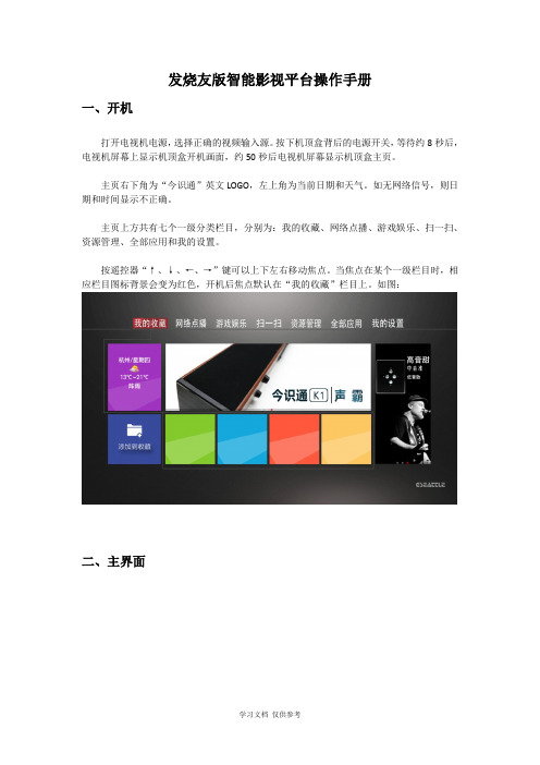
发烧友版智能影视平台操作手册一、开机打开电视机电源,选择正确的视频输入源。
按下机顶盒背后的电源开关,等待约8秒后,电视机屏幕上显示机顶盒开机画面,约50秒后电视机屏幕显示机顶盒主页。
主页右下角为“今识通”英文LOGO,左上角为当前日期和天气。
如无网络信号,则日期和时间显示不正确。
主页上方共有七个一级分类栏目,分别为:我的收藏、网络点播、游戏娱乐、扫一扫、资源管理、全部应用和我的设置。
按遥控器“↑、↓、←、→”键可以上下左右移动焦点。
当焦点在某个一级栏目时,相应栏目图标背景会变为红色,开机后焦点默认在“我的收藏”栏目上。
如图:二、主界面项目类别主要功能我的收藏收藏常用软件网络点播可点击进入网络点播电视软件游戏娱乐可点击进入游戏软件扫一扫进入可扫一扫网络购物资源管理文件管理全部应用全部应用软件我的设置基础设置三、我的收藏添加应用软件的快捷方式到收藏栏将光标移动到“添加到收藏”栏目图标上,点击“OK”键进入,显示全部应用,选取你想要添加到收藏的应用软件,点击“OK”键,图标背景呈绿色,则添加收藏成功,点击返回后可看到快捷方式,收藏栏可添加四个常用应用软件。
如图:四、网络点播点播栏目主要提供频道回看和视频点播应用。
在主页状态下,移动焦点框到“网络点播”栏目,再按“OK”键进入,通过“↑、↓、←、→”键和“OK”键可以进入到某个具体的点播节目,按“返回”键退回上级菜单。
如图:五、游戏娱乐该模块下可创建游戏软件快捷方式。
游戏添加:点击显示机顶盒内的全部应用,选取你想添加到快捷方式的游戏应用软件,图标背景呈绿色,即添加成功,点击返回后可看到快捷方式。
如图:六、扫一扫该模块主要提供在线购物应用。
页面下包含六大类:1、精品男装,2、时尚女装,3、美容护肤,4、数码家电,5、母婴儿童,6、户外运动。
选择每一个模块图标即可显示该类别的商品及其二维码,可进行扫码购物。
通过按遥控器“↑、↓、←、→”键和“OK”键进入到具体栏目和内容,按“返回”键返回上一级菜单或退出该应用,按遥控器“↑”或“↓”键可以快捷翻页。
机顶盒生产流程
机顶盒的生产流程大致分为以下几个环节:
1. 元器件采购:采购各种电子元器件,包括CPU、内存、存储器、电源等。
2. PCB设计:根据产品需求,设计机顶盒的电路板,包括布线、布局等。
3. 制作电路板:将设计好的电路板进行制作,包括印刷电路板(PCB)的制作、电路板组装等步骤。
4. 组装装配:将制作好的电路板与其他部件进行组装装配,包括外壳、按键等。
5. 烧录软件:将机顶盒所需的软件进行烧录,包括操作系统、应用程序等。
6. 测试调试:对已装配好的机顶盒进行功能测试和性能调试,确保机顶盒正常运行。
7. 产品包装:将测试调试通过的机顶盒进行包装,包括外包装、内部保护材料、配件等。
8. 品质检验:对包装好的机顶盒进行品质检验,包括外观检查、功能检查等。
9. 运输发货:将通过品质检验的机顶盒进行运输并发货给销售商或客户。
10. 售后服务:提供售后服务和技术支持,包括维修、更新软件等。
以上是机顶盒的一般生产流程,不同厂商和产品可能会有细微差别。
X X X X X X单位X X X X X X X项目软件需求规格说明书目录第一章引言 (5)1编写目的 (5)2软件需求分析理论 (5)3软件需求分析目标 (5)4参考文献 (6)第二章需求概述 (7)1.项目背景 (7)2.需求概述 (7)3.条件与限制(可选) (8)4.移动办公系统结构 (8)5.移动办公网络拓扑图 (9)第三章系统功能需求 (10)1.移动办公系统升级改造需求 (10)✓界面显示要求 (11)✓待办公文列表 (11)✓待办公文列表排序 (12)✓公文详细信息界面元素 (12)✓网站信息审批 (12)✓会议申请 (12)✓意见录入 (12)✓移动邮件 (13)✓会议管理 (13)✓通知通告 (13)✓通讯录管理 (14)2.车辆管理模块升级改造需求 (14)✓系统功能架构 (14)✓网络拓扑结构 (16)3.电子公文预览需求 (16)✓电子公文交换网络 (17)✓电子公文交换流程 (18)4.政务信息管理系统平台功能需求 (19)第四章软硬件或其他外部系统接口需求 (21)1.用户界面 (21)2.硬件需求 (22)3.网络需求 (22)4.接口需求 (23)5.通信需求 (23)6.运行环境 (24)第五章其他非功能需求 (25)1.性能需求 (25)2.安全设施需求 (25)3.安全性需求 (26)4.扩展性需求 (27)5.可移植性需求 (27)第一章引言1编写目的为明确软件需求、安排项目规划与进度、组织软件开发与测试,撰写本文档。
2软件需求分析理论软件需求分析(Software Reguirement Analysis)是研究用户需求得到的东西,完全理解用户对软件需求的完整功能,确认用户软件功能需求,建立可确认的、可验证的一个基本依据。
软件需求分析是一个项目的开端,也是项目实施最重要的关键点。
据有关的机构分析结果表明,设计的软件产品存在不完整性、不正确性等问题80%以上是需求分析错误所导致的,而且由于需求分析错误造成根本性的功能问题尤为突出。