
931BS-470M中文资料
- 格式:pdf
- 大小:94.64 KB
- 文档页数:1


1.Product profile1.1General descriptionNPN matched double transistor in a SOT363 (SC-88) SMD plastic package. Matched version of BC847BS. The transistors are fully isolated internally.PNP equivalent: BCM857BS.1.2Featuress Current gain matchings Base-emitter voltage matching1.3Applicationss Current mirrors Differential amplifier1.4Quick reference dataBCM847BSNPN matched double transistor;∆h FE =10 %Rev. 02 — 6 April 2005Product data sheetTable 1:Quick reference data Symbol ParameterConditions Min Typ Max Unit V CEO collector-emitter voltage open base--45V I C collector current --100mAh FE DC current gain V CE = 5 V;I C =2mA 200290450∆h FE h FE matching V CE = 5 V;I C =2mA --10%∆V BEV BE matchingV CE = 5 V;I C =2mA --2mV2.Pinning information3.Ordering information4.Marking[1]* = -: made in Hong Kong * = p: made in Hong Kong * = t: made in Malaysia * = W: made in ChinaTable 2:PinningPin Description Simplified outlineSymbol1emitter TR12base TR13collector TR24emitter TR25base TR26collector TR1132456sym02021356TR1TR24Table 3:Ordering informationType numberPackage NameDescriptionVersion BCM847BSSC-88plastic surface mounted package; 6leadsSOT363Table 4:Marking codesType number Marking code [1]BCM847BSM1*5.Limiting values[1]Device mounted on an FR4 Printed-Circuit Board (PCB), single-sided copper, tin-plated and standard footprint.6.Thermal characteristics[1]Device mounted on an FR4 PCB, single-sided copper, tin-plated and standard footprint.Table 5:Limiting valuesIn accordance with the Absolute Maximum Rating System (IEC 60134).Symbol ParameterConditions Min Max Unit Per transistorV CBO collector-base voltage open emitter -50V V CEO collector-emitter voltage open base -45V V EBO emitter-base voltage open collector -6V I C collector current (DC)-100mA I CM peak collector current single pulse;t p ≤1ms -200mA P tot total power dissipation T amb ≤ 25°C-200mW T stg storage temperature −65+150°C T j junction temperature -150°C T amb ambient temperature −65+150°C Per device P tottotal power dissipationT amb ≤ 25°C[1]-300mWTable 6:Thermal characteristics Symbol ParameterConditions Min Typ Max Unit Per deviceR th(j-a)thermal resistance from junction to ambientin free air[1]--416K/W7.Characteristics[1]Pulse test: t p ≤ 300µs;δ≤ 0.02.Table 7:CharacteristicsT amb = 25°C unless otherwise specified.Symbol Parameter Conditions Min Typ Max Unit Per transistor I CBOcollector-base cut-off current V CB = 30 V; I E = 0 A --15nA V CB = 30 V; I E = 0 A;T j =150°C --5µA I EBO emitter-base cut-off current V EB = 5 V; I C = 0 A --100nAh FEDC current gain V CE = 5 V; I C = 10µA -250-V CE = 5 V; I C = 2 mA200290450V CEsat collector-emitter saturation voltage I C = 10 mA; I B = 0.5 mA -50200mV I C = 100 mA; I B = 5 mA [1]-200400mV V BEsat base-emittersaturation voltage I C = 10 mA; I B = 0.5 mA -760-mV I C = 100 mA; I B = 5 mA -910-mV V BE base-emitter voltageV CE = 5 V; I C = 2 mA 610660710mV V CE = 5 V; I C = 10 mA--770mV C c collector capacitance V CB = 10 V; I E = i e = 0 A;f =1MHz -- 1.5pF C e emitter capacitance V EB =0.5V;I C =i c =0A;f =1MHz-11-pF f Ttransition frequencyV CE = 5 V; I C = 10 mA;f =100MHz 100250-MHzPer device ∆h FE DC current gain matchingV CE = 5 V; I C = 2 mA --10%∆V BEbase-emitter voltage matchingV CE = 5 V; I C = 2 mA--2mV8.Package outline9.Packing information[1]For further information and the availability of packing methods, see Section 14.[2]T1: normal taping [3]T2: reverse tapingFig 1.Package outline SOT363 (SC-88)04-11-08Dimensions in mm0.250.100.30.2pin 1index1.30.652.22.0 1.351.152.21.8 1.10.80.450.15132465Table 8:Packing methodsThe indicated -xxx are the last three digits of the 12NC ordering code.[1]Type number Package DescriptionPacking quantity 300010000BCM847BSSOT3634 mm pitch, 8 mm tape and reel; T1[2]-115-1354 mm pitch, 8 mm tape and reel; T2[3]-125-16510.Revision historyTable 9:Revision historyDocument ID Release date Data sheet status Change notice Doc. number Supersedes BCM847BS_220050406Product data sheet-9397 750 14722BCM847BS_1 Modifications:•Table7 Revaluation of data according to the latest control samples•Table7 I CBO unit for conditions V CB = 30 V; I E = 0 A; T j = 150°C amended toµABCM847BS_120040914Product data sheet-9397 750 13711-11.Data sheet status[1]Please consult the most recently issued data sheet before initiating or completing a design.[2]The product status of the device(s) described in this data sheet may have changed since this data sheet was published. The latest information is available on the Internet at URL .[3]For data sheets describing multiple type numbers, the highest-level product status determines the data sheet status.12.DefinitionsShort-form specification —The data in a short-form specification is extracted from a full data sheet with the same type number and title. For detailed information see the relevant data sheet or data handbook.Limiting values definition — Limiting values given are in accordance with the Absolute Maximum Rating System (IEC 60134). Stress above one or more of the limiting values may cause permanent damage to the device.These are stress ratings only and operation of the device at these or at any other conditions above those given in the Characteristics sections of the specification is not implied. Exposure to limiting values for extended periods may affect device reliability.Application information — Applications that are described herein for any of these products are for illustrative purposes only. Philips Semiconductors make no representation or warranty that such applications will be suitable for the specified use without further testing or modification.13.DisclaimersLife support —These products are not designed for use in life support appliances, devices, or systems where malfunction of these products can reasonably be expected to result in personal injury. Philips Semiconductors customers using or selling these products for use in such applications do so at their own risk and agree to fully indemnify Philips Semiconductors for any damages resulting from such application.Right to make changes —Philips Semiconductors reserves the right to make changes in the products - including circuits, standard cells, and/or software - described or contained herein in order to improve design and/or performance. When the product is in full production (status ‘Production’),relevant changes will be communicated via a Customer Product/Process Change Notification (CPCN). Philips Semiconductors assumes noresponsibility or liability for the use of any of these products, conveys no license or title under any patent, copyright, or mask work right to theseproducts,and makes no representations or warranties that these products are free from patent,copyright,or mask work right infringement,unless otherwise specified.14.Contact informationFor additional information, please visit: For sales office addresses, send an email to: sales.addresses@Level Data sheet status [1]Product status [2][3]DefinitionI Objective data Development This data sheet contains data from the objective specification for product development. Philips Semiconductors reserves the right to change the specification in any manner without notice.IIPreliminary dataQualificationThis data sheet contains data from the preliminary specification.Supplementary data will be published at a later date.Philips Semiconductors reserves the right to change the specification without notice,in order to improve the design and supply the best possible product.III Product data ProductionThis data sheet contains data from the product specification. Philips Semiconductors reserves the right to make changes at any time in order to improve the design,manufacturing and supply.Relevant changes will be communicated via a Customer Product/Process Change Notification (CPCN).15.Contents1Product profile. . . . . . . . . . . . . . . . . . . . . . . . . . 11.1General description. . . . . . . . . . . . . . . . . . . . . . 11.2Features . . . . . . . . . . . . . . . . . . . . . . . . . . . . . . 11.3Applications . . . . . . . . . . . . . . . . . . . . . . . . . . . 11.4Quick reference data. . . . . . . . . . . . . . . . . . . . . 12Pinning information. . . . . . . . . . . . . . . . . . . . . . 23Ordering information. . . . . . . . . . . . . . . . . . . . . 24Marking. . . . . . . . . . . . . . . . . . . . . . . . . . . . . . . . 25Limiting values. . . . . . . . . . . . . . . . . . . . . . . . . . 36Thermal characteristics. . . . . . . . . . . . . . . . . . . 37Characteristics. . . . . . . . . . . . . . . . . . . . . . . . . . 48Package outline . . . . . . . . . . . . . . . . . . . . . . . . . 59Packing information. . . . . . . . . . . . . . . . . . . . . . 510Revision history. . . . . . . . . . . . . . . . . . . . . . . . . 611Data sheet status. . . . . . . . . . . . . . . . . . . . . . . . 712Definitions . . . . . . . . . . . . . . . . . . . . . . . . . . . . . 713Disclaimers. . . . . . . . . . . . . . . . . . . . . . . . . . . . . 714Contact information . . . . . . . . . . . . . . . . . . . . . 7© Koninklijke Philips Electronics N.V.2005All rights are reserved.Reproduction in whole or in part is prohibited without the priorwritten consent of the copyright owner.The information presented in this document doesnot form part of any quotation or contract,is believed to be accurate and reliable and maybe changed without notice.No liability will be accepted by the publisher for anyconsequence of its use.Publication thereof does not convey nor imply any license underpatent- or other industrial or intellectual property rights.Date of release: 6 April 2005Document number: 9397 750 14722。

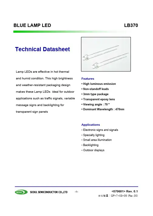
LM78M12中⽂资料LM341/LM78MXX Series3-Terminal Positive Voltage RegulatorsGeneral DescriptionThe LM341and LM78MXX series of three-terminal positive voltage regulators employ built-in current limiting,thermal shutdown,and safe-operating area protection which makes them virtually immune to damage from output overloads.With adequate heatsinking,they can deliver in excess of 0.5A output current.Typical applications would include local (on-card)regulators which can eliminate the noise and de-graded performance associated with single-point regulation.Featuresn Output current in excess of 0.5A n No external componentsn Internal thermal overload protection n Internal short circuit current-limitingn Output transistor safe-area compensationnAvailable in TO-220,TO-39,and TO-252D-PAK packagesn Output voltages of 5V,12V,and 15VConnection DiagramsTO-39Metal Can Package (H)DS010484-5Bottom ViewOrder Number LM78M05CH,LM78M12CH or LM78M15CHSee NS Package Number H03ATO-220Power Package (T)DS010484-6Top ViewOrder Number LM341T-5.0,LM341T-12,LM341T-15,LM78M05CT,LM78M12CT or LM78M15CTSee NS Package Number T03BTO-252DS010484-19Top ViewOrder Number LM78M05CDT See NS Package Number TD03BJuly 1999LM341/LM78MXX Series 3-Terminal Positive Voltage Regulators1999National Semiconductor Corporation /doc/96ef4d46852458fb770b5641.htmlAbsolute Maximum Ratings(Note1)If Military/Aerospace specified devices are required, please contact the National Semiconductor Sales Office/ Distributors for availability and specifications.Lead Temperature(Soldering,10seconds)TO-39Package(H)300?C TO-220Package(T)260?C Storage Temperature Range?65?C to+150?C Operating Junction TemperatureRange?40?C to+125?C Power Dissipation(Note2)Internally Limited Input Voltage5V≤V O≤15V35V ESD Susceptibility TBDElectrical CharacteristicsLimits in standard typeface are for T J=25?C,and limits in boldface type apply over the?40?C to+125?C operating temperature range.Limits are guaranteed by production testing or correlation techniques using standard Statistical Quality Control(SQC) methods.LM341-5.0,LM78M05CUnless otherwise specified:V IN=10V,C IN=0.33µF,C O=0.1µFSymbol Parameter Conditions Min Typ Max Units V O Output Voltage I L=500mA 4.8 5.0 5.2V5mA≤I L≤500mA 4.75 5.0 5.25P D≤7.5W,7.5V≤V IN≤20VV R LINE Line Regulation7.2V≤V IN≤25V I L=100mA50mVI L=500mA100V R LOAD Load Regulation5mA≤I L≤500mA100I Q Quiescent Current I L=500mA410.0mA ?I Q Quiescent Current Change5mA≤I L≤500mA0.57.5V≤V IN≤25V,I L=500mA 1.0V n Output Noise Voltage f=10Hz to100kHz40µVElectrical CharacteristicsLimits in standard typeface are for T J=25?C,and limits in boldface type apply over the?40?C to+125?C operating temperature range.Limits are guaranteed by production testing or correlation techniques using standard Statistical Quality Control(SQC) methods.(Continued)LM341-12,LM78M12CUnless otherwise specified:V IN=19V,C IN=0.33µF,C O=0.1µFSymbol Parameter Conditions Min Typ Max UnitsV O Output Voltage I L=500mA11.51212.5V5mA≤I L≤500mA11.41212.6P D≤7.5W,14.8V≤V IN≤27VV R LINE Line Regulation14.5V≤V IN≤30V I L=100mA120mVI L=500mA240V R LOAD Load Regulation5mA≤I L≤500mA240I Q Quiescent Current I L=500mA410.0mAI Q Quiescent Current Change5mA≤I L≤500mA0.514.8V≤V IN≤30V,I L=500mA 1.0V n Output Noise Voltage f=10Hz to100kHz75µVRipple Rejection f=120Hz,I L=500mA69dBV IN Input Voltage Required I L=500mA17.6V to Maintain Line RegulationV O Long Term Stability I L=500mA60mV/khrs Note1:Absolute maximum ratings indicate limits beyond which damage to the component may occur.Electrical specifications do not apply when operating the de-vice outside of its rated operating conditions.Note2:The typical thermal resistance of the three package types is:T(TO-220)package:θ(JA)=60?C/W,θ(JC)=5?C/WH(TO-39)package:θ(JA)=120?C/W,θ(JC)=18?C/WDT(TO-252)package:θ(JA)=92?C/W,θ(JC)=10?C/W3/doc/96ef4d46852458fb770b5641.htmlSchematic DiagramDS010484-1 /doc/96ef4d46852458fb770b5641.html 4 Typical Performance CharacteristicsPeak Output CurrentDS010484-10Ripple RejectionDS010484-11Ripple RejectionDS010484-12Dropout VoltageDS010484-13Output Voltage(Normalizedto1V at T J=25?C)DS010484-14Quiescent CurrentDS010484-15/doc/96ef4d46852458fb770b5641.html 5Typical Performance Characteristics(Continued)Design ConsiderationsThe LM78MXX/LM341XX fixed voltage regulator series has built-in thermal overload protection which prevents the de-vice from being damaged due to excessive junction tem-perature.The regulators also contain internal short-circuit protection which limits the maximum output current,and safe-area pro-tection for the pass transistor which reduces the short-circuit current as the voltage across the pass transistor is in-creased.Although the internal power dissipation is automatically lim-ited,the maximum junction temperature of the device must be kept below +125?C in order to meet data sheet specifica-tions.An adequate heatsink should be provided to assure this limit is not exceeded under worst-case operating condi-tions (maximum input voltage and load current)if reliable performance is to be obtained).1.0Heatsink ConsiderationsWhen an integrated circuit operates with appreciable cur-rent,its junction temperature is elevated.It is important to quantify its thermal limits in order to achieve acceptable per-formance and reliability.This limit is determined by summing the individual parts consisting of a series of temperature rises from the semiconductor junction to the operating envi-ronment.A one-dimension steady-state model of conduction heat transfer is demonstrated in The heat generated at thedevice junction flows through the die to the die attach pad,through the lead frame to the surrounding case material,to the printed circuit board,and eventually to the ambient envi-ronment.Below is a list of variables that may affect the ther-mal resistance and in turn the need for a heatsink.R θJC (Component Variables)R θCA (Application Variables)Leadframe Size &Material Mounting Pad Size,Material,&LocationNo.of Conduction Pins Placement of Mounting Pad Die SizePCB Size &Material Die Attach MaterialTraces Length &WidthMolding Compound Size and MaterialAdjacent Heat Sources Volume of Air Air FlowAmbient Temperature Shape of Mounting PadQuiescent CurrentDS010484-16Output ImpedanceDS010484-17Line Transient Response DS010484-7Load Transient ResponseDS010484-8/doc/96ef4d46852458fb770b5641.html6Design Considerations(Continued)The LM78MXX/LM341XX regulators have internal thermal shutdown to protect the device from over-heating.Under all possible operating conditions,the junction temperature of the LM78MXX/LM341XX must be within the range of 0?C to 125?C.A heatsink may be required depending on the maxi-mum power dissipation and maximum ambient temperature of the application.To determine if a heatsink is needed,the power dissipated by the regulator,P D ,must be calculated:I IN =I L +I GP D =(V IN ?V OUT )I L +V IN I Gshows the voltages and currents which are present in the circuit.The next parameter which must be calculated is the maxi-mum allowable temperature rise,T R (max):θJA =TR (max)/P D If the maximum allowable value for θJA ?C/w is found to be ≥60?C/W for TO-220package or ≥92?C/W for TO-252pack-age,no heatsink is needed since the package alone will dis-sipate enough heat to satisfy these requirements.If the cal-culated value for θJA fall below these limits,a heatsink is required.As a design aid,Table 1shows the value of the θJA of TO-252for different heatsink area.The copper patterns that we used to measure these θJA are shown at the end of the Application Note Section.reflects the same test results as what are in the Table 1shows the maximum allowable power dissipation vs.ambi-ent temperature for theTO-252device.shows the maximum allowable power dissipation vs.copper area (in 2)for the TO-252device.Please see AN1028for power enhancement techniques to be used with TO-252package.TABLE 1.θJA Different Heatsink AreaLayoutCopper AreaThermal Resistance Top Sice (in 2)*Bottom Side (in 2)(θJA ,?C/W)TO-25210.0123010320.06608730.306040.5305450.7605261047700.284800.470900.6631000.857110157120.0660.06689130.1750.17572140.2840.28461150.3920.39255160.50.553*Tab of device attached to topside copperDS010484-23FIGURE 1.Cross-sectional view of Integrated Circuit Mounted on a printed circuit board.Note that the case temperature is measured at the point where the leadscontact with the mounting pad surface DS010484-24FIGURE 2.Power Dissipation Diagram/doc/96ef4d46852458fb770b5641.html 7Design Considerations(Continued)Typical ApplicationDS010484-20FIGURE 3.θJA vs.2oz Copper Area for TO-252DS010484-22FIGURE 4.Maximum Allowable Power Dissipation vs.Ambient Temperature for TO-252DS010484-21FIGURE 5.Maximum Allowable Power Dissipation vs.2oz.Copper Area for TO-252DS010484-9*Required if regulator input is more than 4inches from input filter capacitor (or if no input filter capacitor is used).**Optional for improved transient response./doc/96ef4d46852458fb770b5641.html 8 Physical Dimensions inches(millimeters)unless otherwise notedTO-39Metal Can Package(H)Order Number LM78M05CH,LM78M12CH or LM78M15CHNS Package Number H03A9/doc/96ef4d46852458fb770b5641.htmlPhysical Dimensions inches(millimeters)unless otherwise noted(Continued)TO-220Power Package(T)Order Number LM341T-5.0,LM341T-12,LM341T-15,LM78M05CT,LM78M12CT or LM78M15CT NS Package Number T03B/doc/96ef4d46852458fb770b5641.html 10Physical Dimensionsinches (millimeters)unless otherwise noted (Continued)LIFE SUPPORT POLICYNATIONAL’S PRODUCTS ARE NOT AUTHORIZED FOR USE AS CRITICAL COMPONENTS IN LIFE SUPPORT DEVICES OR SYSTEMS WITHOUT THE EXPRESS WRITTEN APPROVAL OF THE PRESIDENT AND GENERAL COUNSEL OF NATIONAL SEMICONDUCTOR CORPORATION.As used herein:1.Life support devices or systems are devices or systems which,(a)are intended for surgical implant into the body,or (b)support or sustain life,and whose failure to perform when properly used in accordance with instructions for use provided in the labeling,can be reasonably expected to result in a significant injury to the user.2.A critical component is any component of a life support device or system whose failure to perform can be reasonably expected to cause the failure of the life support device or system,or to affect its safety or effectiveness.National Semiconductor Corporation AmericasTel:1-800-272-9959Fax:1-800-737-7018Email:support@/doc/96ef4d46852458fb770b5641.htmlNational Semiconductor EuropeFax:+49(0)180-5308586Email:europe.support@/doc/96ef4d46852458fb770b5641.htmlDeutsch Tel:+49(0)180-5308585English Tel:+49(0)180-5327832Fran?ais Tel:+49(0)180-5329358Italiano Tel:+49(0)180-5341680National Semiconductor Asia Pacific Customer Response Group Tel:65-2544466Fax:65-2504466Email:sea.support@/doc/96ef4d46852458fb770b5641.htmlNational Semiconductor Japan Ltd.Tel:81-3-5639-7560Fax:81-3-5639-7507/doc/96ef4d46852458fb770b5641.htmlTO-252Order Number LM78M05CDT NS Package Number TD03BLM341/LM78MXX Series 3-Terminal Positive Voltage RegulatorsNational does not assume any responsibility for use of any circuitry described,no circuit patent licenses are implied and National reserves the right at any time without notice to change said circuitry andspecifications.。
本人使用过程中翻译了本文,水平有限难免有误,欢迎纠正:tyooo@A49313-Phase Brushless DC Motor Pre-Driver三相无刷直流电机前置驱动器4931-DS, Rev. 4下载::/~/media/Files/Datasheets/A4931-Datasheet.ashx下载翻译:2012-11-15▪ ▪ ▪ ▪▪▪ ▪▪本人使用过程中翻译了本文,水平有限难免有误,欢迎纠正: tyooo@A4931 三相无刷直流电机前置驱动器Absolute Maximum RatingsThermal Characteristics*For additional information, refer to the Allegro website.CharacteristicSymbolNotes RatingUnits供电电压Load Supply Voltage V BB38 V 电机输出Motor Phase Output S X t w < 500 ns –3 V 霍尔输入 V Hx DC–0.3 to 7 V 逻辑输入电压范围 V IN–0.3 to 7 V 工作环境温度 T A Range M–20 to 105ºC 最大结温度 T J (max) 150 ºC 储藏温度T stg–40 to 150ºCCharacteristicSymbolTest Conditions*RatingUnits封装内阻,结点到外面(Junction to Ambient )R θJA 4-layer PCB based on JEDEC standard32 ºC/W 封装内阻,结点到焊盘(Junction to Exposed Pad )R θJP2ºC/W本人使用过程中翻译了本文,水平有限难免有误,欢迎纠正: tyooo@A4931 三相无刷直流电机前置驱动器Functional Block DiagramTerminal List0.1 μFNumber 1Name HA+ Description Hall input A 2 HA - Hall input A 3 HB+ Hall input B 4 HB Hall input B 5 HC+ Hall input C 6 HC- Hall input C 7 GND Ground8 HBIAS Hall bias power supply output 9 CP1 Charge pump capacitor terminal 10 CP2 Charge pump capacitor terminal 11 VBB Supply voltage12 VCP Reservoir capacitor terminal 13 SENSE Sense resistor connection 14GLCLow side gate drive CNumber 15 Name GLB Description Low side gate drive B 16 GLA Low side gate drive A 17 GHC High side gate drive C18 SC High side source connection C 19 GHB High side gate drive B20 SB High side source connection B 21 GHA High side gate drive A22 SA High side source connection A 23 FG1 FG 1 speed control output (3 Φ inputs)24 FG2 FG 2 speed control output (ΦA input) 25 CLD Locked rotor detect timing capacitor 26 DIR Logic input – motor direction27 ENABLE Logic input – external PWM control 28BRAKEZLogic input – motor brake (active low)本人使用过程中翻译了本文,水平有限难免有误,欢迎纠正: tyooo@A4931 三相无刷直流电机前置驱动器ELECTRICAL CHARACTERISTICS *Valid at T A= 25°C, V BB= 24 V, unless noted otherwise*Typical data are for initial design estimations only, and assume optimum manufacturing and application conditions. Performance may vary for individualunits, within the specified maximum and minimum limits. For input and output current specifications, negative current is defined as coming out of (sourcing) the specified device pin. Specifications throughout the allowed operating temperature range are guaranteed by design and characterization.本人使用过程中翻译了本文,水平有限难免有误,欢迎纠正:tyooo@ A4931 三相无刷直流电机前置驱动器本人使用过程中翻译了本文,水平有限难免有误,欢迎纠正:tyooo@固定断开时间Fixed Off-Time 理论上A4931的固定断开本人使用过程中翻译了本文,水平有限难免有误,欢迎纠正:tyooo@ A4931 三相无刷直流电机前置驱动器ET Package, 28-Contact QFNFor Reference Only (reference JEDEC MO-220VHHD-1) Dimensions in millimeters Exact caseand lead configuration at supplier discretion within limits shown0.55 +0.20 –0.10Terminal #1 mark area 3.15Exposed thermal pad (reference only, terminal #1 identifier appearance at supplier discretion)Reference land pattern layout (reference IPC7351 QFN50P500X500X100-29V1M); All pads a minimum of 0.20 mm from all adjacentpads; adjust as necessary to meet application process requirements and PCB layout tolerances; when mounting on a multilayer PCB,thermal vias at the exposed thermal pad land can improve thermal dissipation (reference EIA/JEDEC Standard JESD51-5)Coplanarity includes exposed thermal本人使用过程中翻译了本文,水平有限难免有误,欢迎纠正:tyooo@总结1.BREAK:低电平进入刹车状态。