
TA8814中文资料
- 格式:pdf
- 大小:610.64 KB
- 文档页数:15

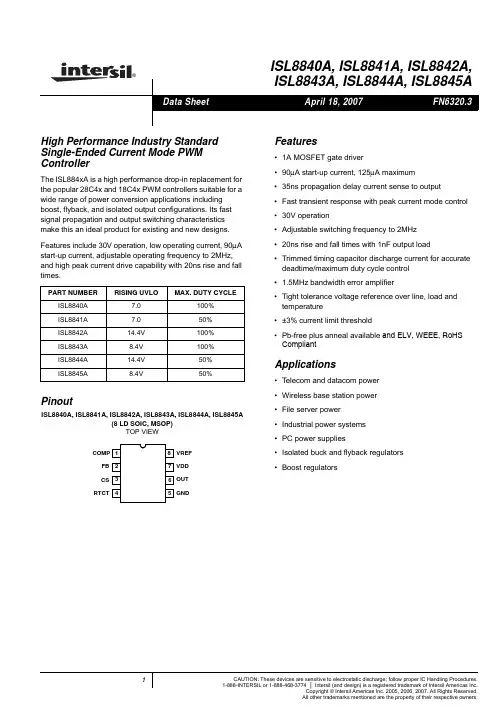

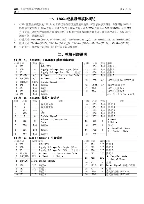
型号功能ACP2371NI 多制式数字音频信号处理电路ACVP2205 梳状滤波、视频信号处理电路AN5071 波段转换控制电路AN5195K 子图像信号处理电路AN5265 伴音功率放大电路AN5274 伴音功率放大电路AN5285K 伴音前置放大电路AN5342K 图像水平轮廓校正、扫描速度调制电路AN5348K AI信号处理电路AN5521 场扫描输出电路AN5551 枕形失真校正电路AN5560 50/60Hz场频自动识别电路AN5612 色差、基色信号变换电路AN5836 双声道前置放大及控制电路AN5858K TV/AV切换电路AN5862K(AN5862S) 视频模拟开关AN5891K 音频信号处理电路AT24C02 2线电可擦、可编程只读存储器AT24C04 2线电可擦、可编程只读存储器AT24C08 2线电可擦、可编程只读存储器ATQ203 扬声器切换继电器电路BA3880S 高分辨率音频信号处理电路BA3884S 高分辨率音频信号处理电路BA4558N 双运算放大器BA7604N 梳状切换开关电路BU9252S 8bitA/D转换电路CAT24C16 2线电可擦、可编程只读存储器CCU-FDTV 微处理器CCU-FDTV-06 微处理器CD54573A/CD54573CS 波段转换控制电路CH0403-5H61 微处理器CH04801-5F43 微处理器CH05001(PCA84C841) 微处理器CH05002 微处理器CH7001C 数字NTSC/PAL编码电路CHT0406 微处理器CHT0803(TMP87CP38N*) 8bit微处理器CHT0807(TMP87CP38N) 8bit微处理器CHT0808(TMP87CP38N) 8bit微处理器CHT0818 微处理器CKP1003C 微处理器CKP1004S(TMP87CK38N) 微处理器CKP1006S(TMP87CH38N) 微处理器CKP1008S(TMP87CK38N/F) 微处理器CKP1009S(TMP87CH38N) 微处理器CKP1105S(Z90231) 微处理器CKP1301S(TMP87CH38N) 微处理器CKP1403S 微处理器CM0006CF 数字会聚校正电路CNX62A 光电耦合器CNX82A 光电耦合器CPF8598 存储器CTV222S.PRC1.2 微处理器CTV225S-PRC1 微处理器CTV591S.GW3 微处理器CXA1545AS TV/AV多路切换电路CXA1642P 背景歌声消除电路CXA1686M 时钟信号发生器CXA1779P 基色信号处理电路CXP1103S-9919EP 微处理器CXP750096 微处理器CXP85332-108A 微处理器DM8361 单片集成TV小信号处理电路DPU2553/DPU2554 偏转信号处理电路DTI2251 数字色信号过渡特性改善电路GAL16V8C 同步信号变换电路GD74LS10 三组3输入与非门GD74LS393 双4位二进制计数器GD74LS74A 双D触发器GM99200B 微处理器HA11508 图像及伴音信号转换控制电路HCF4046B 低功耗通用锁相环电路HCF4052B 双4选1模拟开关HCF4053BE 三组2路模拟开关HCT157 VGA信号与TV/AV同步信号切换电路HCT4046AD 低功耗通用锁相环电路HD14066 四组双向模拟开关HD14066B 四组双向模拟开关HD14066BP 四组双向模拟开关HEF4052 双4选1模拟开关HEF4053 三组2路模拟开关HEF4094 8级移位-存储总线寄存器HIC1015 开关电源稳压控制及保护电路HIC1016 开关电源稳压控制及保护电路HIC1026 保护模块HM4864P-12 随机存取存储器HPD6325C D/A转换电路HS0038 遥控信号接收电路IX0823GE 微处理器IX1763CEN1 单片集成TV小信号处理电路JLC1562BF 总线控制输入/输出口扩展电路K6274K/D 图像中频带通滤波器K9450M 伴音第一中频带通滤波器KA2107 音频控制电路KA2500 宽带视频放大电路KA3S0680R 开关电源专用厚膜电路KA3S0880RFB 开关电源专用厚膜电路KA7630 多路稳压输出电路KB2511B 数字偏转电路KONKA266(P83C266) 微处理器KS88C3216 微处理器KS88C8324 微处理器L7805 5V固定正稳压器L7808 8V固定正稳压器L7812 12V固定正稳压器L78LR05/L78LR05D/L78LR50-MA/L78M05F/L78M05FA/L78MR05/L78MR05FA 5V稳压复位电路L78OSO5FA 5V可控稳压电路L7912 9V固定负稳压器L7918 18V固定负稳压器LA2785 杜比逻辑处理电路LA4225 5W音频功率放大电路LA4261 立体声功率放大电路LA4270 6W×2音频功率放大电路LA4280 10W×2音频功率放大电路LA4282 10W×2音频功率放大电路LA4445 双声道音频功率放大电路LA6358 双运算放大器LA7016 电子开关LA7210 同步检测电路LA7222 二回路、二接点电子开关LA7406 画中画接口电路LA7575 图像中频放大电路LA76810 TV小信号处理电路LA76832N TV小信号处理电路LA7685 中频及图像信号处理电路LA7838 场扫描电路LA7840 场扫描输出电路LA7841 场扫描输出电路LA7845 场扫描输出电路LA7845N 场扫描输出电路LA7846N 场扫描输出电路LA7910 波段转换控制电路LA7950 场频识别控制电路LA7954 视频转换电路LC344250Z 多端动态存储器LC74401E 画中画(PIP)控制电路LC78815M 双通道16bitD/A变换电路LC863316A 微处理器LC863320A 微处理器LC863328A 微处理器LC863348A 微处理器LC864512 微处理器LC864512V-5D18 微处理器LC864512V-5C77 微处理器LC864525 微处理器LC864916A 微处理器LM317 稳压器LM324 四运算放大器LM358 双运算放大器LM567 锁相环电路LUKS-5140-M2 微处理器LV1010N 杜比逻辑处理电路 M32L1632512A 同步图形存储器M34300N-587SP 微处理器M34300N4-555SP 微处理器M37210M3-508SP 微处理器M37210M3-800SP 多制式数字音频信号处理电路M37210M3-902SP 微处理器M37210M4-705SP 微处理器M37211M2-609SP 微处理器M37220M3 微处理器M37221M6-065SP 微处理器M37222M6-084SP 微处理器M37225 微处理器M37270MF-168SP 微处理器M37271MP-209SP 微处理器M37274EFSP 微处理器M37280 微处理器M37551MA-0545SP 微处理器M50436-688SP 微处理器M51131L 话筒演唱及混响音量控制电路M5218AP 双运算放大器M52340SP 单片集成TV小信号处理电路M52470AP 三通道4输入模拟开关M54573L 波段转换控制电路M62354FP 六通道8bitD/A转换电路M62438FP SRSM65839SP 数字式卡拉OK信号处理电路M66312P PIP控制电路M6M80011P 存储器M6M80041P 存储器MALF24C01 存储器MALF24C02 存储器MB3110A 超低音频信号处理电路MB81461-12RS 动态随机存储器MC14066BCP 四组双向模拟开关MC141625A 梳状滤波器MC141628 前置亮、色信号分离梳状滤波器MC144110P D/A转换电路MC14577C 双视频放大电路MC33064D5 复位用欠压检测电路MC44608 开关稳压电源电压模式控制器MC68HC16R1(SC43402CFC) 微处理器MCM6206BBE 32K×8bit快速静态随机存取存储器MCU2600 时钟信号发生器MM1031XS 宽带视频放大电路MM1053XS 多路信号高速切换电路MM1113XS 多路信号高速切换电路MM1495XD A/V切换电路MN1515TWE/TWP 微处理器MN152810TTD5 微处理器MN152811TIX 微处理器MN15282 微处理器MN1871675T6S 微处理器MN1871675T7M 微处理器MN1872432TWI 微处理器MN187-681 微处理器MN3868 1H基带延迟线电路MSP3410 多制式丽音解码电路MSP3410B 多制式丽音解码电路MSP3410D 多制式丽音解码电路MSP3410D-52 多制式丽音解码电路MSP3410D-CS 多制式丽音解码电路MSP3410D-PP-B4 多制式丽音解码电路MSP3410D-P0-B4 多制式丽音解码电路MSP3415D-AI I*IC总线控制多制式音频处理电路MSP3463G 音频信号处理电路NE5532N 内部补偿低噪声双运算放大器NE/SE567 音调与频率解码、锁相环电路NE567N 音调与频率解码、锁相环电路NJM2234L 伴音声道控制开关NJM2700L WOW音频处理电路NJW1103 杜比定向逻辑和音色选择电路NJW1132AL 伴音BBE处理电路NM24C04EN 存储器NN5099K/NN5199K 单片集成多制式TV小信号处理电路NP83C266BRNA 微处理器NV320P 数字视频信号处理电路NVM3060 存储器OM8361 单片集成TV小信号处理电路OM8361-VS0469 单片集成TV小信号处理电路OM8839 I*IC总线控制单片集成TV小信号处理电路OM8839PS I*IC总线控制单片集成TV小信号处理电路OM8839PS-K9G216 I*IC总线控制单片集成TV小信号处理电路ONWA KWEC42.2ONWA KWEC44.1OTT531 +5V稳压复位电路P83C266BDR 微处理器P87C766 微处理器P87C766BDR(CKP1401S) 微处理器P87C766DT 微处理器PC74HT241P 线性驱动数据缓冲电路PC713F6 光耦合器PCA841P-177 微处理器PCA84C122/PCA84C222/PCA84C422/PCA84C622/ PCA84C822 PCA84C440P/401 微处理器PCA84C641 微处理器PCA84C840P-054 微处理器PCA8516 字符形成电路PCA8521 遥控编码发射电路PCA8521BT 遥控编码发射电路PCF8581P 存储器PCF8582 存储器PCF8589C-2 存储器PCF8594C-2 存储器PCF8598 E2PROM存储器PCF8598C-2 E2PROM存储器PCF8598E E2PROM存储器PCX8598X-2 E2PROM存储器PIP2250 PIP信号处理电路PQ05RF 受控+5V稳压器PQ09RD11(78HR09) 受控+9V稳压器PQ12RF 受控+12V稳压器PQ12RF2 受控+12V稳压器S24C08A 存储器SAA3010T 遥控信号发射电路SAA4955TJ 场存储器SAA4955TS 数字式场存储器SAA4956TJ 具有降噪功能的场存储器SAA4961 PAL/NTSC兼容梳状滤波器SAA4977H 倍场频处理电路SAA4981 单片集成16:9压缩处理电路SAA4991WP 运动估算和补偿、降低行间闪烁、变焦和降噪电路SAA5284 多媒体视频数据捕获电路SAA5700GP 汉字系统图文电视(CCST)解码电路SAA7280P 丽音信号处理电路SAA7283ZP 丽音解调解码电路SAB9077H PIP控制电路SBX1765-01 数字梳状滤波器SDA9187 PIPSDA9187-2X PIPSDA9189X 1/4屏幕多画面PIP处理电路SDA9205 三路8bitA/D转换电路SDA9220 存储同步控制电路SDA9251 存储器SDA9257 时钟同步发生器SDA9280 显示信号处理电路SDA9288 PIP/POP信号处理电路SDA9288X PIP/POP信号处理电路SDA9290 数字图像处理电路SDA9361 DDC-PLUS偏转控制电路SDA9362 扫描小信号处理电路SDA9400 扫描变换处理电路SE110N 开关电源误差信号放大电路SE116E 开关电源误差信号放大电路SE140N/SE145N 开关电源误差信号放大电路SECL810 音频信号控制电路SID2500-DOBO R、G、B混合处理电路SKW011-829A2202 微处理器SMM-201N 微处理器ST24C02 2线电可擦、可编程只读存储器ST24C04 2线电可擦、可编程只读存储器ST63156 微处理器ST6367B1/FEJ 微处理器ST92196 微处理器STK392-040 三通道会聚校正放大电路STK392-110 三通道会聚校正放大电路STR-6658B 开关电源厚膜电路STR-D1005T 开关电源厚膜电路STR-F6454 开关电源厚膜电路STR-F6653 开关电源厚膜电路STR-F6654 开关电源厚膜电路STR-F6656 开关电源厚膜电路STR-F6658B 开关电源厚膜电路STR-F6707 开关电源厚膜电路STR-G8656 开关电源厚膜电路STR-M6529F04 开关电源厚膜电路STR-M6833BF04 开关电源厚膜电路STR-S5941 开关电源厚膜电路STR-S6308 开关电源厚膜电路STR-S6309 开关电源厚膜电路STR-S6709 开关电源厚膜电路STR-S6709A 开关电源厚膜电路STR-S6709AN 开关电源厚膜电路STR-Z3202 开关电源厚膜电路STR-Z4302 开关电源厚膜电路STR-Z4479 开关电源厚膜电路STV2116 视频解码电路STV2246 I*IC总线控制单片集成TV小信号处理电路STV2248 I*IC总线控制单片集成TV小信号处理电路STV5111 R、G、B高压视频放大电路STV5112 R、G、B高压视频放大电路STV9306 场扫描输出电路STV9379 场扫描输出电路T7808CT 8V固定正稳压器TA1216AN 三通道音频信号处理电路TA1218AN AV/TV切换电路TA1219AN AV/TV切换电路TA1219N AV/TV切换电路TA1222AN 多制式视频、色度、同步、偏转信号处理电路TA1222BN 多制式视频、色度、同步、偏转信号处理电路TA1226N 亮度信号瞬态校正电路TA1229N SECAM制解码电路TA1270BF PAL/NTSC视频和色信号处理电路TA1316AN 逐行扫描倍场频画质增强电路TA1318N 多制式扫描行场振荡电路TA2009P 数字信号滤波电路TA2047N 丽音系统模拟滤波电路TA2136F/N 声音重演信号(SRS)处理电路TA24C04/TA24C08/TL24C04 2线电可擦、可编程只读存储器TA7347P S端子切换电路TA7439 三波段数字控制音频信号切换及处理电路TA7508P 四运算放大器TA75393S 双电压比较器TA75458P 双运算放大器TA7555F/P 时间延时器TA75558P 双运算放大器TA75559P 双运算放大器TA7809S 9V固定正稳压器TA78L09AP 9V固定正稳压器TA8173AP 双声道立体环绕声处理电路TA8200AH 双声道音频功率放大电路TA8211AH 双声道音频功率放大电路TA8213K 重低音功率放大电路TA8218AH 音频功率放大电路TA8256H 6W×3通道音频功率放大电路TA8256HV 三通道音频功率放大电路TA8258H 双通道音频功率放大电路TA8403K 场扫描输出电路TA8427K 场扫描输出电路TA8445K 场扫描输出电路TA8615N 制式转换电路TA8628N 带电子音量控制的AV/TV开关电路TA8659BN 多制式视频、偏转、文字显示信号处理及制式转换电路TA8710S 伴音中频转换电路TA8720AN TV/AV(S-VHS)切换电路TA8765N SECAM解码电路TA8772AN PAL/NTSC/SECAM基带1H延迟电路TA8772CN PAL/NTSC/SECAM基带1H延迟电路TA8776N 环绕声信号处理电路TA8777NFA-1 PIP画面视频信号选择开关TA8795AF PIP画面多制式亮度、色度、同步信号处理电路TA8814N 彩色瞬态特性改善电路TA8815BN 模拟视频信号选择开关TA8851AN 双极型I*IC总线控制AV开关TA8851BN 双极型I*IC总线控制AV开关TA8851CN 双极型I*IC总线控制AV开关TA8859CP 枕形失真校正电路TA8859P 枕形失真校正电路TA8880CN 视频、色度、同步信号处理电路TA8889P I*IC总线控制白平衡调整电路TAIF24C04 存储器TB1204N 丽音信号处理电路TB1212N 丽音信号处理电路TB1227AN PAL/NTSC/SECAM视频、色度、扫描小信号处理电路TB1227N PAL/NTSC/SECAM视频、色度、扫描小信号处理电路TB1227 PAL/NTSC/SECAM视频、色度、扫描小信号处理电路TB1231N 视频、色度、扫描小信号处理电路TB1238AN 视频、色度、扫描小信号处理电路TB1238N 视频、色度、扫描小信号处理电路TB1240N I*IC总线控制TV信号处理电路TB1240AN I*IC总线控制TV信号处理电路TBA2800 遥控信号接收电路TC4052 双4选1模拟开关TC4052B 双4选1模拟开关TC4052BP 双4选1模拟开关TC4053 三组2路双向模拟开关TC4053AP/TC4053BP 三组2路双向模拟开关TC4066AF 四组双向模拟开关TC4094BP 端口扩展电路TC74HC4053AP 三组2路双向模拟开关TC74HC4066AF 四组双向模拟开关TC9028F 遥控信号发射电路TC9083F/P 单片PIP控制电路TC9089 数字Y/C信号分离电路TC9090AN 多制式3行数字Y/C信号分离电路TC9090CN 多制式3行数字Y/C信号分离电路TC9090N/F 多制式3行数字Y/C信号分离电路TC9097F 彩色信号处理电路TC90A49P 多制式3行数字Y/C信号分离电路TC9415N 数字卡拉OK电路TDA1521 双通道伴音功率放大电路TDA1521A 双通道伴音功率放大电路TDA1524A 立体声(音量/音调)控制电路TDA1543 数控变换电路TDA16846 开关电源厚膜电路T DA2007 6W×2音频功率放大电路TDA2007A 6W×2音频功率放大电路TDA2009A 10W×2双路音频功率放大电路TDA2030 14WTDA2595 行、场扫描及同步脉冲发生器TDA2616 带静音功能的12W×2TDA3504 视频控制、矩阵电路TDA3654 场扫描输出电路TDA3857 准分离伴音解码电路TDA4472 TV信号前置处理电路TDA4505 彩色电视小信号处理电路TDA4555 多制式色度解码电路TDA4565 亮度延迟、彩色暂态特性改善电路TDA4601 开关电源厚膜电路TDA4605 开关电源厚膜电路TDA4605-3 开关电源厚膜电路TDA4665 基带彩色信号延迟电路TDA4671 彩色瞬态改善(CTI)电路TDA4681 矩阵变换及亮度控制电路TDA4780 视频信号处理电路TDA4853/TDA4854 I*IC总线自同步偏转控制电路TDA5112 单片视频放大输出电路TDA5330T 高频调谐器专用贴片电路TDA6101Q 视频放大输出电路TDA6103Q 视频放大输出电路TDA6107Q 视频放大输出电路TDA6108JF 单片视频放大输出电路TDA6110Q 视频放大输出电路TDA6111Q 视频放大输出电路TDA6120Q 宽带视频放大输出电路TDA6151 卫星电视接收视频处理电路TDA7056A/TDA7056B 超重低音功率放大电路TDA7057AQ 双声道音频功率放大电路TDA7265 双通道音频功率放大电路TDA7297 双声道功率放大电路TDA7429S 立体声信号切换、处理电路TDA7496 带直流音量控制的双通道音频功率放大电路TDA8133 具有“禁止”和复位功能的+5.1V、+8V稳压器TDA8139 具有CPU复位功能的稳压电路TDA8145 光栅东/西失真校正电路TDA8170 场扫描输出电路TDA8172 场扫描输出电路TDA8177F 场扫描输出电路TDA8179 场扫描输出电路TDA8219 色度信号解码电路TDA8305A 图像中放电路TDA8310 PIPTDA8310A PIP全制式色度信号处理电路TDA8341 内载波中频信号处理电路TDA8350Q 直流耦合场偏转和东/西枕校输出电路TDA8351 场扫描输出电路TDA8351AQ 场扫描输出电路TDA8354 宽范围场扫描输出电路TDA8361 PAL/NTSC单片集成TV小信号处理电路TDA8362 单片集成全制式TV小信号处理电路TDA8366N3D 单片集成TV小信号处理电路TDA8376A I*IC总线控制多制式TV小信号处理电路TDA8395 SECAM色度解码电路TDA8425 Hi-Fi音频信号处理电路TDA8540 视频4×4开关矩阵切换电路TDA8732 丽音信号处理电路TDA8814N 亮度、色度信号处理电路TDA8838 I*IC总线控制单片集成TV小信号处理电路TDA8839 I*IC总线控制单片集成TV小信号处理电路TDA8841 I*IC总线控制多制式TV小信号处理电路TDA8843 I*IC总线控制PAL/NTSC制单片集成TV小信号处理电路TDA8844 I*IC总线控制多制式单片集成TV小信号处理电路TDA8944J Hi-Hi立体声功率放大电路TDA8945J 音频功率放大电路TDA9111 行、场扫描信号处理电路TDA9143 解码/同步信号处理电路TDA9151B 可编程扫描控制电路TDA9160 多制式解码/同步信号处理电路TDA9170 亮度改善和色度信号校正处理电路TDA9177 亮度、色差信号瞬态校正电路TDA9178 YUV画质改善处理电路TDA9181 多制式集成梳状滤波器TDA9302H 场扫描输出电路TDA9321 I*IC总线控制TV小信号处理电路TDA9321H 主画面TV信号处理电路TDA9332H I*IC总线控制TV显示处理电路TDA9370 CPU+TV超级电视信号处理电路TDA9380 MCU+VCD超级芯片电视信号处理电路TDA9383 CPU+TV超级电视信号处理电路TDA9429S 音频信号切换及处理电路TDA9801 中频锁相环解调和鉴频器TDA9808 准声像分离,PLL鉴频中频处理电路TDA9808T 准声像分离,PLL鉴频中频处理电路TDA9815 多路中频信号处理电路TDA9859 Hi-Fi音频信号处理电路TDA9860 Hi-Fi音频信号处理电路TDA9874A 数字伴音解调和解码电路TEA2014A 视频信号切换开关TEA5114A 视频信号切换开关TEA5170 同步、稳压电源电路TEA6415B I*IC总线控制视频矩阵开关TEA6415C I*IC总线控制视频矩阵开关TEA6420 I*IC总线控制音频矩阵开关TEA6430 I*IC总线控制音频矩阵开关TLC29321PWL 高效锁相环电路TLP621 光电耦合器TMP83C266BDR-100 微处理器TMP87CH33N 微处理器TMP87CH36 微处理器TMP87CH38N 微处理器TMP87CK38N-3644 微处理器TMP87CM36N 微处理器TMP87CM38N 微处理器TMP87CP38N 微处理器TMP87CS38N 微处理器TMP87PM36N-R0605 微处理器TMP87PS38N 微处理器TMS73C45TKY2 A1检测(模糊逻辑)电路TNY254P 5V待机电路TPU2735 图文电视处理电路TVSM5218L 双声道音频功率放大电路VCT3803A/01A CPU+TV超级电视信号处理电路VCU2133 视频A/D与D/A编解码电路VCU2136 数字视频信号处理电路VDP3108A 数字视频及偏转信号处理电路VDP3120C 数字视频、显示及偏转信号处理电路VPC3215C 数字视频信号处理电路VSP2860 数字视频及同步信号处理电路WH2000(WUHAN2000) 微处理器WH2000C 微处理器XR1075 BBE音响增强处理电路Z86227 微处理器Z90361 微处理器μPC1830GT 视频、色度及扫描小信号处理电路μPC1853 移相矩阵环绕声处理电路μPC1853-01 移相矩阵环绕声处理电路μPC1891Y/A 矩阵环绕声信号处理电路μPC2412HF +12V稳压电路μPD6124 红外线遥控发射电路μPD6325C 6位D/A转换电路μPD6336C 6位D/A转换电路μPD6375 D/A转换电路μPD6376 D/A转换电路10K2 SRS音效处理器14577B 双通道带宽放大电路24C08 存储器24C04-4A99A819 存储器24WC16P 存储器4052 双4选1模拟开关47-00001-42(29022306) 微处理器47C1638AU353 微处理器47C834N-RB11 微处理器74HC86/74HCT86 四组2输入异或门74HC157/74HCT157 四组2选1数据选择器74HC573D 三态输出8位透明D型锁存器74HC4046A/74HCT4046A 低功耗锁相环VCO电路74HC4066 双向模拟电子开关74HC4538D/74HCT4538D 双路可重新触发单稳态多谐振荡器74HCT241N 线性驱动数据缓冲器74LS9D 六路施密特触发倒向器74LS10 三组3输入与非门74LS74 双D触发器(带置位、复位、正触发)74LS393 双4位二进制计数器。

FEATURES DESCRIPTIONAPPLICATIONSR FBI OUTGNDV DDV REFCSCLKSDIDAC8811SLAS411A–NOVEMBER2004–REVISED DECEMBER2004 16-Bit,Serial Input Multiplying Digital-to-Analog Converter•±0.5LSB DNL The DAC8811multiplying digital-to-analog converter •16-Bit Monotonic(DAC)is designed to operate from a single2.7-V to5.5-V supply.•±1LSB INL•Low Noise:12nV/√Hz The applied external reference input voltage VREFdetermines the full-scale output current.An internal •Low Power:I DD=2µAfeedback resistor(R FB)provides temperature tracking •+2.7V to+5.5V Analog Power Supplyfor the full-scale output when combined with an •2mA Full-Scale Current±20%,external I-to-V precision amplifier.with V REF=10VA serial data interface offers high-speed,three-wire•50-MHz Serial Interfacemicrocontroller-compatible inputs using data-in(SDI),•0.5µs Settling Time clock(CLK),and chip-select(CS).•4-Quadrant Multiplying ReferenceThe DAC8811is packaged in space-saving8-lead •Reference Bandwidth:10MHzSON and MSOP packages.•±10V Reference Input•Reference Dynamics:-105THD•Tiny8-Lead3x3mm SON and3x5mmMSOP Packages•Industry-Standard Pin Configuration•Automatic Test Equipment•Instrumentation•Digitally Controlled Calibration•Industrial Control PLCsPlease be aware that an important notice concerning availability,standard warranty,and use in critical applications of TexasInstruments semiconductor products and disclaimers thereto appears at the end of this data sheet.PRODUCTION DATA information is current as of publication date.Copyright©2004,Texas Instruments Incorporated Products conform to specifications per the terms of the TexasInstruments standard warranty.Production processing does notnecessarily include testing of all parameters.元器件交易网ABSOLUTE MAXIMUM RATINGSDAC8811SLAS411A–NOVEMBER 2004–REVISED DECEMBER 2004This integrated circuit can be damaged by ESD.Texas Instruments recommends that all integratedcircuits be handled with appropriate precautions.Failure to observe proper handling and installation procedures can cause damage.ESD damage can range from subtle performance degradation to complete device failure.Precision integrated circuits may be more susceptible to damage because very small parametric changes could cause the device not to meet its published specifications.PACKAGE/ORDERING INFORMATION (1)MINIMUM RELATIVE DIFFERENTIAL PACKAGE-SPECIFIED TRANSPORT ACCURACYNONLINEARITYLEADTEMPERATUREPACKAGE ORDERING MEDIA,PRODUCT (LSB)(LSB)(DESIGNATOR)RANGE MARKINGNUMBER QUANTITY DAC8811C ±1±1MSOP-8(DGK)-40°C to +85°C D11DAC8811ICDGKT Tape and Reel,250DAC8811C ±1±1MSOP-8(DGK)-40°C to +85°C D11DAC8811ICDGKR Tape and Reel,2500DAC8811C ±1±1SON-8(DRB)-40°C to +85°C D11DAC8811ICDRBT Tape and Reel,250DAC8811C ±1±1SON-8(DRB)-40°C to +85°C D11DAC8811ICDRBR Tape and Reel,2500DAC8811B ±2±1MSOP-8(DGK)-40°C to +85°C D11DAC8811IBDGKT Tape and Reel,250DAC8811B ±2±1MSOP-8(DGK)-40°C to +85°C D11DAC8811IBDGKR Tape and Reel,2500DAC8811B ±2±1SON-8(DRB)-40°C to +85°C D11DAC8811IBDRBT Tape and Reel,250DAC8811B±2±1SON-8(DRB)-40°C to +85°CD11DAC8811IBDRBRTape and Reel,2500(1)For the most current specifications and package information,see the Package Option Addendum located at the end of this data sheet or refer to our web site at .over operating free-air temperature range (unless otherwise noted)(1)DAC8811UNIT V DD to GND-0.3to +7V Digital input voltage to GND -0.3to +V DD +0.3V V (I OUT )to GND-0.3to +V DD +0.3V Operating temperature range -40to +105°C Storage temperature range-65to +150°C Junction temperature range (T J max)+125°CPower dissipation (T J max -T A )/R ΘJAThermal impedance,R ΘJA 55°C/W Lead temperature,soldering Vapor phase (60s)215°C Lead temperature,soldering Infrared (15s)220°C ESD rating,HBM 1500V ESD rating,CDM 1000V (1)Stresses above those listed under absolute maximum ratings may cause permanent damage to the device.Exposure to absolute maximum conditions for extended periods may affect device reliability.2元器件交易网ELECTRICAL CHARACTERISTICSDAC8811 SLAS411A–NOVEMBER2004–REVISED DECEMBER2004V DD =+2.7V to+5.5V;IOUT=Virtual GND,GND=0V;VREF=10V;TA=full operating temperature.All specifications-40°Cto+85°C,unless otherwise noted.DAC8811PARAMETER CONDITIONS MIN TYP MAX UNITS STATIC PERFORMANCE(1)Resolution16BitsRelative accuracy DAC8811C±1LSBRelative accuracy DAC8811B±2LSBDifferential nonlinearity±1LSBOutput leakage current Data=0000h,T A=+25°C10nAOutput leakage current Data=0000h,T A=T MAX10nAFull-scale gain error All ones loaded to DAC register±1±4mVFull-scale tempco±3ppm/°COUTPUT CHARACTERISTICS(2)Output current2mAOutput capacitance Code dependent50pFREFERENCE INPUTVREF Range-1515VInput resistance5kΩInput capacitance5pFLOGIC INPUTS AND OUTPUT(2)Input low voltage V IL V DD=+2.7V0.6VV IL V DD=+5V0.8V Input high voltage V IH V DD=+2.7V 2.1VV IH V DD=+5V 2.4V Input leakage current I IL10µAInput capacitance C IL10pFINTERFACE TIMINGClock input frequency f CLK50MHzClock pulse width high10nsClock pulse width low10nsCS to Clock setup time0nsClock to CS hold time10nsData setup time5nsData hold time10nsPOWER REQUIREMENTSV DD 2.7 5.5VI DD(normal operation)Logic inputs=0V5µAV DD=+4.5V to+5.5V V IH=V DD and V IL=GND35µAV DD=+2.7V to+3.6V V IH=V DD and V IL=GND1 2.5µAAC CHARACTERISTICSOutput voltage settling time0.5µsReference multiplying BW V REF=5V PP,Data=FFFFh10MHzV REF=0V to10V,DAC glitch impulse2nV/sData=7FFFh to8000h to7FFFhFeedthrough error V OUT/V REF Data=0000h,V REF=100kHz-70dBDigital feedthrough2nV/s(1)Linearity calculated using a reduced code range of48to4047;output unloaded.(2)Specified by design and characterization;not production tested.3元器件交易网 PIN ASSIGNMENTSDRB PACKAGEDGK PACKAGER VR VDAC8811SLAS411A–NOVEMBER2004–REVISED DECEMBER2004 ELECTRICAL CHARACTERISTICS(continued)V DD =+2.7V to+5.5V;IOUT=Virtual GND,GND=0V;VREF=10V;TA=full operating temperature.All specifications-40°Cto+85°C,unless otherwise noted.DAC8811PARAMETER CONDITIONS MIN TYP MAX UNITS Total harmonic distortion-105dBOutput spot noise voltage12nV/√HzTable1.TERMINAL FUNCTIONSPIN NAME DESCRIPTION1CLK Clock input;positive edge triggered clocks data into shift registerSerial register input;data loads directly into the shift register MSB first.Extra 2SDIleading bits are ignored.3R FB Internal matching feedback resistor.Connect to external op amp output.DAC reference input pin.Establishes DAC full-scale voltage.Constant input 4V REFresistance versus code.DAC current output.Connects to inverting terminal of external precision I/V op 5I OUTamp.6GND Analog and digital ground.7V DD Positive power supply input.Specified operating range of2.7V to5.5V.Chip-select;active low digital input.Transfers shift register data to DAC register 8CSon rising edge.See Table2for operation.4元器件交易网TYPICAL CHARACTERISTICS:V DD =+5V1.00.80.60.40.20−0.2−0.4−0.6−0.8−1.0819216384245763276840960495125734465536I N L (L S B )Digital Input CodeT A =+25_C1.00.80.60.40.20−0.2−0.4−0.6−0.8−1.0D N L (L S B )T A =+25_C819216384245763276840960495125734465536Digital Input Code1.00.80.60.40.20−0.2−0.4−0.6−0.8−1.0T A =−40_CD N L (L S B )819216384245763276840960495125734465536Digital Input Code1.00.80.60.40.20−0.2−0.4−0.6−0.8−1.0T A =−40_CI N L (L S B )819216384245763276840960495125734465536Digital Input Code1.00.80.60.40.20−0.2−0.4−0.6−0.8−1.0I N L (L S B )T A =+85_C819216384245763276840960495125734465536Digital Input Code 1.00.80.60.40.20−0.2−0.4−0.6−0.8−1.0D N L (L S B )T A =+85_C819216384245763276840960495125734465536Digital Input CodeDAC8811SLAS411A–NOVEMBER 2004–REVISED DECEMBER 2004At T A =+25°C,+V DD =+5V,unless otherwise noted.LINEARITY ERROR DIFFERENTIAL LINEARITY ERRORvs DIGITAL INPUT CODEvs DIGITAL INPUT CODEFigure 1.Figure 2.LINEARITY ERROR DIFFERENTIAL LINEARITY ERRORvs DIGITAL INPUT CODEvs DIGITAL INPUT CODEFigure 3.Figure 4.LINEARITY ERROR DIFFERENTIAL LINEARITY ERRORvs DIGITAL INPUT CODEvs DIGITAL INPUT CODEFigure 5.Figure 6.5元器件交易网1.61.41.21.00.80.60.40.2000.51.01.52.02.53.03.54.04.55.0Logic Input Voltage (V)S u p p l y C u r r e n t , I D D (m A )60−6−12−18−24−30−36−42−48−54−60−66−72−78−84−90−96−102−108−114101001k10k100k1M10M100MA t t e n u a t i o n (dB )Bandwidth(Hz)Time (0.1µs/div)O u t p u t V o l t a g e (5V /d i v )Time (0.2µs/div)O u t p u t V o l t a g e (50m V /d i v )DAC8811SLAS411A–NOVEMBER 2004–REVISED DECEMBER 2004TYPICAL CHARACTERISTICS:V DD =+5V (continued)At T A =+25°C,+V DD =+5V,unless otherwise noted.SUPPLY CURRENTvs LOGIC INPUT VOLTAGEREFERENCE MULTIPLYING BANDWIDTHFigure 7.Figure 8.DAC GLITCHDAC SETTLING TIMEFigure 9.Figure 10.6元器件交易网TYPICAL CHARACTERISTICS:V DD =+2.7V1.00.80.60.40.20−0.2−0.4−0.6−0.8−1.0I N L (L S B )T A =+25_C819216384245763276840960495125734465536Digital Input Code1.00.80.60.40.20−0.2−0.4−0.6−0.8−1.0D N L (L S B )T A =+25_C819216384245763276840960495125734465536Digital Input Code1.00.80.60.40.20−0.2−0.4−0.6−0.8−1.0T A =−40_CI N L (L S B )819216384245763276840960495125734465536Digital Input Code T A =−40_C1.00.80.60.40.20−0.2−0.4−0.6−0.8−1.0D N L (L S B )819216384245763276840960495125734465536Digital Input Code1.00.80.60.40.20−0.2−0.4−0.6−0.8−1.0I N L (L S B )T A =+85_C819216384245763276840960495125734465536Digital Input Code 1.00.80.60.40.20−0.2−0.4−0.6−0.8−1.0D N L (L S B )T A =+85_C819216384245763276840960495125734465536Digital Input CodeDAC8811SLAS411A–NOVEMBER 2004–REVISED DECEMBER 2004At T A =+25°C,+V DD =+2.7V,unless otherwise noted.LINEARITY ERROR DIFFERENTIAL LINEARITY ERRORvs DIGITAL INPUT CODEvs DIGITAL INPUT CODEFigure 11.Figure 12.LINEARITY ERROR DIFFERENTIAL LINEARITY ERRORvs DIGITAL INPUT CODEvs DIGITAL INPUT CODEFigure 13.Figure 14.LINEARITY ERROR DIFFERENTIAL LINEARITY ERRORvs DIGITAL INPUT CODEvs DIGITAL INPUT CODEFigure 15.Figure 16.7元器件交易网THEORY OF OPERATIONV REFGNDI OUTV OUT +*V REF CODE65536(1)V OV REFDAC8811SLAS411A–NOVEMBER 2004–REVISED DECEMBER 2004The DAC8811is a single channel current output,16-bit digital-to-analog converter (DAC).The architecture,illustrated in Figure 17,is an R-2R ladder configuration with the three MSBs segmented.Each 2R leg of the ladder is either switched to GND or the I OUT terminal.The I OUT terminal of the DAC is held at a virtual GND potential by the use of an external I/V converter op amp.The R-2R ladder is connected to an external reference input V REF that determines the DAC full-scale current.The R-2R ladder presents a code independent load impedance to the external reference of 5k Ω±25%.The external reference voltage can vary in a range of -15V to 15V,thus providing bipolar I OUT current operation.By using an external I/V converter and the DAC8811R FB resistor,output voltage ranges of -V REF to V REF can be generated.Figure 17.Equivalent R-2R DAC CircuitWhen using an external I/V converter and the DAC8811R FB resistor,the DAC output voltage is given by Equation 1:Each DAC code determines the 2R leg switch position to either GND or I OUT .Because the DAC outputimpedance as seen looking into the I OUT terminal changes versus code,the external I/V converter noise gain will also change.Because of this,the external I/V converter op amp must have a sufficiently low offset voltage such that the amplifier offset is not modulated by the DAC I OUT terminal impedance change.External op amps with large offset voltages can produce INL errors in the transfer function of the DAC8811due to offset modulation versus DAC code.For best linearity performance of the DAC8811,an op amp (OPA277)is recommended (Figure 18).This circuit allows V REF swinging from -10V to +10V.Figure 18.Voltage Output Configuration8元器件交易网SDI CLKCSAPPLICATION INFORMATIONStabilityCircuitV OUTPositive Voltage Output CircuitDAC8811SLAS411A–NOVEMBER 2004–REVISED DECEMBER 2004THEORY OF OPERATION (continued)Figure 19.DAC8811Timing Diagram Table 2.Control Logic Truth Table (1)CLK CS Serial Shift Register DAC Register X H No effectLatched ↑+L Shift register data advanced one bit Latched X H No effectLatchedX ↑+Shift register data transferred to DAC registerNew data loaded from serial register(1)↑+Positive logic transition;X =Don't careTable 3.Serial Input Register Data Format,Data Loaded MSB FirstB15B0Bit (MSB)B14B13B12B11B10B9B8B7B6B5B4B3B2B1(LSB)DataD15D14D13D12D11D10D9D8D7D6D5D4D3D2D1D0For a current-to-voltage design (see Figure 20),the DAC8811current output (I OUT )and the connection with the inverting node of the op amp should be as short as possible and according to correct PCB layout design.For each code change there is a step function.If the GBP of the op amp is limited and parasitic capacitance is excessive at the inverting node then gain peaking is possible.Therefore,for circuit stability,a compensation capacitor C1(4pF to 20pF typ)can be added to the design,as shown in Figure 20.Figure 20.Gain Peaking Prevention Circuit With Compensation CapacitorAs Figure 21illustrates,in order to generate a positive voltage output,a negative reference is input to the DAC8811.This design is suggested instead of using an inverting amp to invert the output due to tolerance errors of the resistor.For a negative reference,V OUT and GND of the reference are level-shifted to a virtual ground and a -2.5V input to the DAC8811with an op amp.9元器件交易网V OUTBipolar Output CircuitV OUT+ǒD32,768*1ǓV REF(2)V OUT10 k W10 k W+2.5V(+10V)Programmable Current Source CircuitI L +(R2)R3)ńR1R3VREFD(3)DAC8811SLAS411A–NOVEMBER2004–REVISED DECEMBER2004APPLICATION INFORMATION(continued)Figure21.Positive Voltage Output CircuitThe DAC8811,as a2-quadrant multiplying DAC,can be used to generate a unipolar output.The polarity of the full-scale output I OUT is the inverse of the input reference voltage at V REF.Some applications require full4-quadrant multiplying capabilities or bipolar output swing.As shown in Figure22, external op amp U4is added as a summing amp and has a gain of2X that widens the output span to5V.A 4-quadrant multiplying circuit is implemented by using a 2.5-V offset of the reference voltage to bias U4.According to the circuit transfer equation given in Equation2,input data(D)from code0to full scale produces output voltages of V OUT=-2.5V to V OUT=+2.5V.External resistance mismatching is the significant error in Figure22.Figure22.Bipolar Output CircuitA DAC8811can be integrated into the circuit in Figure23to implement an improved Howland current pump forprecise voltage to current conversions.Bidirectional current flow and high voltage compliance are two features of the circuit.With a matched resistor network,the load current of the circuit is shown by Equation3:10元器件交易网ZO+R1ȀR3(R1)R2)R1(R2Ȁ)R3Ȁ)*R1Ȁ(R2)R3)(4)V REFR244OUTCross-ReferenceDAC8811 SLAS411A–NOVEMBER2004–REVISED DECEMBER2004The value of R3in the previous equation can be reduced to increase the output current drive of U3.U3can drive ±20mA in both directions with voltage compliance limited up to15V by the U3voltage supply.Elimination of the circuit compensation capacitor C1in the circuit is not suggested as a result of the change in the output impedance Z O,according to Equation4:As shown in Equation4,with matched resistors,Z O is infinite and the circuit is optimum for use as a current source.However,if unmatched resistors are used,Z O is positive or negative with negative output impedance being a potential cause of oscillation.Therefore,by incorporating C1into the circuit,possible oscillation problems are eliminated.The value of C1can be determined for critical applications;for most applications,however,a value of several pF is suggested.Figure23.Programmable Bidirectional Current Source CircuitThe DAC8811has an industry-standard pinout.Table4provides the cross-reference information.Table4.Cross-ReferenceSPECIFIEDTEMPERATURE PACKAGE PACKAGE CROSS-PRODUCT INL(LSB)DNL(LSB)RANGE DESCRIPTION OPTION REFERENCE PART DAC8811ICDGK±1±1-40°C to+85°C8-Lead MicroSOIC MSOP-8N/ADAC8811IBDGK±2±1-40°C to+85°C8-Lead MicroSOIC MSOP-8AD5543BRMDAC8811ICDRB±1±1-40°C to+85°C8-Lead Small Outline SON-8N/ADAC8811IBDRD±2±1-40°C to+85°C8-Lead Small Outline SON-8N/A N/A±2±1-40°C to+85°C8-Lead SOIC SOIC-8AD5543BR11元器件交易网PACKAGING INFORMATIONOrderable Device Status (1)Package Type Package Drawing Pins Package Qty Eco Plan (2)Lead/Ball FinishMSL Peak Temp (3)DAC8811IBDGKR ACTIVE MSOP DGK 82500TBD Call TI Call TIDAC8811IBDGKT ACTIVE MSOP DGK 8250TBD Call TILevel-1-220C-UNLIMDAC8811IBDRBR ACTIVE SON DRB 83000TBD CU POST PLATE Level-1-240C-UNLIM DAC8811IBDRBT ACTIVE SON DRB 8250TBD CU POST PLATE Level-1-240C-UNLIMDAC8811ICDGKR ACTIVE MSOP DGK 82500TBD Call TI Level-1-220C-UNLIM DAC8811ICDGKT ACTIVE MSOP DGK 8250TBD Call TI Level-1-220C-UNLIM DAC8811ICDRBR ACTIVE SON DRB 83000TBD CU SNPB Level-1-240C-UNLIM DAC8811ICDRBTACTIVESONDRB8250TBDCU SNPBLevel-1-240C-UNLIM(1)The marketing status values are defined as follows:ACTIVE:Product device recommended for new designs.LIFEBUY:TI has announced that the device will be discontinued,and a lifetime-buy period is in effect.NRND:Not recommended for new designs.Device is in production to support existing customers,but TI does not recommend using this part in a new design.PREVIEW:Device has been announced but is not in production.Samples may or may not be available.OBSOLETE:TI has discontinued the production of the device.(2)Eco Plan -The planned eco-friendly classification:Pb-Free (RoHS)or Green (RoHS &no Sb/Br)-please check /productcontent for the latest availability information and additional product content details.TBD:The Pb-Free/Green conversion plan has not been defined.Pb-Free (RoHS):TI's terms "Lead-Free"or "Pb-Free"mean semiconductor products that are compatible with the current RoHS requirements for all 6substances,including the requirement that lead not exceed 0.1%by weight in homogeneous materials.Where designed to be soldered at high temperatures,TI Pb-Free products are suitable for use in specified lead-free processes.Green (RoHS &no Sb/Br):TI defines "Green"to mean Pb-Free (RoHS compatible),and free of Bromine (Br)and Antimony (Sb)basedflame retardants (Br or Sb do not exceed 0.1%by weight in homogeneous material)(3)MSL,Peak Temp.--The Moisture Sensitivity Level rating according to the JEDEC industry standard classifications,and peak solder temperature.Important Information and Disclaimer:The information provided on this page represents TI's knowledge and belief as of the date that it is provided.TI bases its knowledge and belief on information provided by third parties,and makes no representation or warranty as to the accuracy of such information.Efforts are underway to better integrate information from third parties.TI has taken and continues to take reasonable steps to provide representative and accurate information but may not have conducted destructive testing or chemical analysis on incoming materials and chemicals.TI and TI suppliers consider certain information to be proprietary,and thus CAS numbers and other limited information may not be available for release.In no event shall TI's liability arising out of such information exceed the total purchase price of the TI part(s)at issue in this document sold by TI to Customer on an annual basis.PACKAGE OPTION ADDENDUM17-Jun-2005Addendum-Page 1IMPORTANT NOTICETexas Instruments Incorporated and its subsidiaries (TI) reserve the right to make corrections, modifications, enhancements, improvements, and other changes to its products and services at any time and to discontinue any product or service without notice. Customers should obtain the latest relevant information before placing orders and should verify that such information is current and complete. All products are sold subject to TI’s terms and conditions of sale supplied at the time of order acknowledgment.TI warrants performance of its hardware products to the specifications applicable at the time of sale in accordance with TI’s standard warranty. T esting and other quality control techniques are used to the extent TI deems necessary to support this warranty. Except where mandated by government requirements, testing of all parameters of each product is not necessarily performed.TI assumes no liability for applications assistance or customer product design. Customers are responsible for their products and applications using TI components. T o minimize the risks associated with customer products and applications, customers should provide adequate design and operating safeguards.TI does not warrant or represent that any license, either express or implied, is granted under any TI patent right, copyright, mask work right, or other TI intellectual property right relating to any combination, machine, or process in which TI products or services are used. Information published by TI regarding third-party products or services does not constitute a license from TI to use such products or services or a warranty or endorsement thereof. Use of such information may require a license from a third party under the patents or other intellectual property of the third party, or a license from TI under the patents or other intellectual property of TI.Reproduction of information in TI data books or data sheets is permissible only if reproduction is without alteration and is accompanied by all associated warranties, conditions, limitations, and notices. Reproduction of this information with alteration is an unfair and deceptive business practice. TI is not responsible or liable for such altered documentation.Resale of TI products or services with statements different from or beyond the parameters stated by TI for that product or service voids all express and any implied warranties for the associated TI product or service and is an unfair and deceptive business practice. TI is not responsible or liable for any such statements. Following are URLs where you can obtain information on other Texas Instruments products and application solutions:Products ApplicationsAmplifiers Audio /audioData Converters Automotive /automotiveDSP Broadband /broadbandInterface Digital Control /digitalcontrolLogic Military /militaryPower Mgmt Optical Networking /opticalnetwork Microcontrollers Security /securityTelephony /telephonyVideo & Imaging /videoWireless /wirelessMailing Address:Texas InstrumentsPost Office Box 655303 Dallas, Texas 75265Copyright 2005, Texas Instruments Incorporated。