wm8978中文介绍说明资料
- 格式:doc
- 大小:3.07 MB
- 文档页数:64
LM7818中文资料目录1.lm7818介绍2.实际应用3.引脚序号、引脚功能4.lm7818应用电路5.7818电参数三端稳压集成电路lm7818。
电子产品中,常见的三端稳压集成电路有正电压输出的lm78 ×× 系列和负电压输出的lm79××系列。
顾名思义,三端IC是指这种稳压用的集成电路,只有三条引脚输出,分别是输入端、接地端和输出端。
它的样子象是普通的三极管,TO- 220 的标准封装,也有lm9013样子的TO-92封装。
1.lm7818介绍用lm78/lm79系列三端稳压IC来组成稳压电源所需的外围元件极少,电路内部还有过流、过热及调整管的保护电路,使用起来可靠、方便,而且价格便宜。
该系列集成稳压IC型号中的lm78或lm79后面的数字代表该三端集成稳压电路的输出电压,如lm7806表示输出电压为正6V,lm7909表示输出电压为负9V。
因为三端固定集成稳压电路的使用方便,电子制作中经常采用。
最大输出电流1.5A,LM78XX系列输出电压分别为5V;6V;8V;9V;10V;12V;15V;18V;24V。
2.实际应用在实际应用中,应在三端集成稳压电路上安装足够大的散热器(当然小功率7818IC内部电路图.的条件下不用)。
当稳压管温度过高时,稳压性能将变差,甚至损坏。
当制作中需要一个能输出1.5A以上电流的稳压电源,通常采用几块三端稳压电路并联起来,使其最大输出电流为N个1.5A,但应用时需注意:并联使用的集成稳压电路应采用同一厂家、同一批号的产品,以保证参数的一致。
另外在输出电流上留有一定的余量,以避免个别集成稳压电路失效时导致其他电路的连锁烧毁。
在lm78 ** 、lm79 ** 系列三端稳压器中最常应用的是TO-220 和TO-202 两种封装。
这两种封装的图形以及引脚序号、引脚功能如附图所示。
图中的引脚号标注方法是按照引脚电位从高到底的顺序标注的。


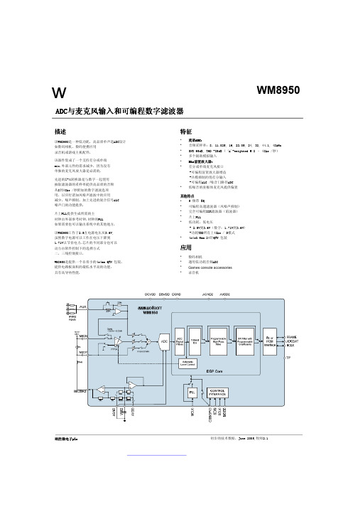
wWM8974Mono CODEC with Speaker DriverWOLFSON MICROELECTRONICS plc Production Data, Rev 4.2 March 2007DESCRIPTIONThe WM8974 is a low power, high quality mono CODEC designed for portable applications such as Digital Still Camera or Digital Voice Recorder.The device integrates support for a differential or single ended mic, and includes drivers for speakers or headphone, and mono line output. External component requirements are reduced as no separate microphone or headphone amplifiers are required.Advanced Sigma Delta Converters are used along with digital decimation and interpolation filters to give high quality audio at sample rates from 8 to 48ks/s. Additional digital filtering options are available in the ADC path, to cater for application filtering such as ‘wind noise reduction’, plus an advanced mixed signal ALC function with noise gate is provided. The digital audio interface supports A-law and µ-law companding. An on-chip PLL is provided to generate the required Master Clock from an external reference clock. The PLL clock can also be output if required elsewhere in the system.The WM8974 operates at supply voltages from 2.5 to 3.6V, although the digital supplies can operate at voltages down to 1.71V to save power. The speaker and mono outputs use a separate supply of up to 5V which enables increased output power if required. Different sections of the chip can also be powered down under software control by way of the selectable two or three wire control interface.WM8974 is supplied in a very small 4x4mm QFN package, offering high levels of functionality in minimum board area, with high thermal performance.FEATURES• Mono CODEC:• Audio sample rates:8, 11.025, 16, 22.05, 24, 32, 44.1, 48kHz • DAC SNR 98dB, THD -84dB (‘A’-weighted @ 8 – 48ks/s) • ADC SNR 94dB, THD -83dB (‘A’-weighted @ 8 – 48ks/s) • On-chip Headphone/Speaker Driver with ‘cap-less’ connect - 40mW output power into 16Ω / 3.3V SPKVDD - BTL speaker drive 0.9W into 8Ω / 5V SPKVDD • Additional MONO Line output• Multiple analog or ‘Aux’ inputs, plus analog bypass path • Mic Preamps:•Differential or single end Microphone Interface - Programmable preamp gain- Psuedo differential inputs with common mode rejection - Programmable ALC / Noise Gate in ADC path •Low-noise bias supplied for electret microphonesOTHER FEATURES• 5 band EQ (record or playback path) • Digital Playback Limiter• Programmable ADC High Pass Filter (wind noise reduction) • Programmable ADC Notch Filter • On-chip PLL• Low power, low voltage- 2.5V to 3.6V (digital: 1.71V to 3.6V)- power consumption <10mA all-on 48ks/s mode • 4x4x0.9mm 24 lead QFN packageAPPLICATIONS• Digital Still Camera Audio Codec• Wireless VoIP and other communication device handsets / headsets• Portable audio recorder•General Purpose low power audio CODECWM8974Production DataTABLE OF CONTENTS DESCRIPTION (1)FEATURES (1)APPLICATIONS (1)TABLE OF CONTENTS (2)PIN CONFIGURATION (3)ORDERING INFORMATION (3)PIN DESCRIPTION (4)ABSOLUTE MAXIMUM RATINGS (5)RECOMMENDED OPERATING CONDITIONS (5)ELECTRICAL CHARACTERISTICS (6)TERMINOLOGY (8)SIGNAL TIMING REQUIREMENTS (9)SYSTEM CLOCK TIMING (9)AUDIO INTERFACE TIMING – MASTER MODE (9)AUDIO INTERFACE TIMING – SLAVE MODE (10)CONTROL INTERFACE TIMING – 3-WIRE MODE (11)CONTROL INTERFACE TIMING – 2-WIRE MODE (12)DEVICE DESCRIPTION (13)INTRODUCTION (13)INPUT SIGNAL PATH (14)ANALOGUE TO DIGITAL CONVERTER (ADC) (19)INPUT LIMITER / AUTOMATIC LEVEL CONTROL (ALC) (23)OUTPUT SIGNAL PATH (35)ANALOGUE OUTPUTS (42)OUTPUT SWITCH (47)DIGITAL AUDIO INTERFACES (49)AUDIO SAMPLE RATES (54)MASTER CLOCK AND PHASE LOCKED LOOP (PLL) (55)GENERAL PURPOSE INPUT/OUTPUT (57)CONTROL INTERFACE (57)RESETTING THE CHIP (58)POWER SUPPLIES (58)POWER MANAGEMENT (63)REGISTER MAP (65)REGISTER BITS BY ADDRESS (66)DIGITAL FILTER CHARACTERISTICS (77)TERMINOLOGY (77)DAC FILTER RESPONSES (78)ADC FILTER RESPONSES (78)DE-EMPHASIS FILTER RESPONSES (79)HIGHPASS FILTER (80)5-BAND EQUALISER (81)APPLICATIONS INFORMATION (85)RECOMMENDED EXTERNAL COMPONENTS (85)PACKAGE DIAGRAM (86)IMPORTANT NOTICE (87)ADDRESS: (87)Production Data WM8974 PIN CONFIGURATIONTOPVIEWORDERING INFORMATIONORDER CODE TEMPERATURERANGE PACKAGE MOISTURESENSITIVITYLEVELPACKAGE BODYTEMPERATUREWM8974GEFL/V -25°C to +85°C 24-lead QFN (4x4x0.9mm)(Pb-free)MSL3 260o CWM8974GEFL/RV -25°C to +85°C 24-lead QFN (4x4x0.9mm)(Pb-free, tape and reel)MSL3 260o C Note:Reel Quantity = 3,500WM8974Production Data PIN DESCRIPTIONPIN NO NAME TYPE DESCRIPTION1 MICBIAS Analogue Output Microphone bias2 AVDD Supply Analogue supply (feeds ADC and DAC)3 AGND Supply Analogue ground (feeds ADC and DAC)4 DCVDD Supply Digital core supply5 DBVDD Supply Digital buffer (input/output) supplyground6 DGND Supply Digital7 ADCDAT Digital Output ADC digital audio data output8 DACDAT Digital Input DAC digital audio data input9 FRAME Digital Input / Output DAC and ADC sample rate clock or frame synch10 BCLK Digital Input / Output Digital audio port clock11 MCLK Digital Input Master clock input12 CSB/GPIO Digital Input / Output 3-Wire MPU chip select or general purpose input/output pin.13 SCLK Digital Input 3-Wire MPU clock Input / 2-Wire MPU Clock Input14 SDIN Digital Input / Output 3-Wire MPU data Input / 2-Wire MPU Data Input15 MODE Digital Input Control interface mode selection pin.Analogue Output Mono output16 MONOOUTAnalogue Output Speaker output positive17 SPKOUTPSupply Speaker ground (feeds speaker and mono output amps only)18 SPKGNDAnalogue Output Speaker output Negative19 SPKOUTNSupply Speaker supply (feeds speaker and mono output amps only)20 SPKVDDAnalogue Input Auxiliary analogue input21 AUXReference Decoupling for midrail reference voltage22 VMIDAnalogue Input Microphone negative input23 MICNAnalogue Input Microphone positive input (common mode)24 MICPNote:It is recommended that the QFN ground paddle should be connected to analogue ground on the application PCB.Production DataWM8974ABSOLUTE MAXIMUM RATINGSAbsolute Maximum Ratings are stress ratings only. Permanent damage to the device may be caused by continuouslyoperating at or beyond these limits. Device functional operating limits and guaranteed performance specifications are given under Electrical Characteristics at the test conditions specified.ESD Sensitive Device. This device is manufactured on a CMOS process. It is therefore generically susceptible to damage from excessive static voltages. Proper ESD precautions must be taken during handling and storage of this device.Wolfson tests its package types according to IPC/JEDEC J-STD-020B for Moisture Sensitivity to determine acceptable storage conditions prior to surface mount assembly. These levels are:MSL1 = unlimited floor life at <30°C / 85% Relative Humidity. Not normally stored in moisture barrier bag. MSL2 = out of bag storage for 1 year at <30°C / 60% Relative Humidity. Supplied in moisture barrier bag. MSL3 = out of bag storage for 168 hours at <30°C / 60% Relative Humidity. Supplied in moisture barrier bag. The Moisture Sensitivity Level for each package type is specified in Ordering Information. CONDITION MIN MAXDBVDD, DCVDD, AVDD supply voltages -0.3V +4.2 SPKVDD supply voltage -0.3V +7V Voltage range digital inputs DGND -0.3V DVDD +0.3V Voltage range analogue inputs AGND -0.3VAVDD +0.3VOperating temperature range, T A -25°C +85°CStorage temperature prior to soldering 30°C max / 85% RH max Storage temperature after soldering -65°C +150°CNotes 1. Analogue and digital grounds must always be within 0.3V of each other. 2. All digital and analogue supplies are completely independent from each other.RECOMMENDED OPERATING CONDITIONSPARAMETER SYMBOL TEST CONDITIONS MIN TYP MAX UNITDigital supply range (Core) DCVDD 1.71 3.6 VDigital supply range (Buffer) DBVDD 1.71 3.6 V Analogue supplies range AVDD 2.5 3.6 VSpeaker supply SPKVDD 2.5 5.5 VGround DGND,AGND,SPKGNDVNotes 1. When using PLL, DCVDD must be 1.9V or higher. 2. AVDD must be ≥ DCVDD.3. DBVDD must be ≥ DCVDD.4. In non-boosted mode, SPKVDD must be ≥ AVDD, if boosted SPKVDD must be ≥ 1.5x AVDD.5.When using PLL, DCVDD must be ≥ 1.9V.WM8974Production DataELECTRICAL CHARACTERISTICSTest ConditionsDCVDD = 1.8V, AVDD = DBVDD = 3.3V, SPKVDD = 3.3V, T A = +25o C, 1kHz signal, fs = 48kHz, 24-bit audio data unless otherwise stated.PARAMETER SYMBOL TEST CONDITIONS MIN TYP MAX UNIT Microphone Inputs (MICN, MICP) Full-scale Input Signal Level (Note 1) – note this changes with AVDDV INFSPGABOOST = 0dB INPPGAVOL = 0dB1.0 0 VrmsdBVMic PGA equivalent input noise At 35.25dBgain 150 uVInput resistance R MICIN Gain set to 35.25dB 1.6 k Ω Input resistance R MICIN Gain set to 0dB 47 k Ω Input resistance R MICIN Gain set to -12dB 75 k Ω Input resistance R MICIP MICP2INPPGA = 1 94 k Ω Input resistance R MICIP MICP2INPPGA = 094k ΩInput Capacitance C MICIN 10 pF MIC Input Programmable Gain Amplifier (PGA)Programmable Gain-12 35.25 dBProgrammable Gain Step Size Guaranteed monotonic0.75dBMute Attenuation 108 dB Selectable Input Gain Boost (0/+20dB)Gain Boost 0 20 dB Automatic Level Control (ALC)/Limiter – ADC onlyTarget Record Level -28.5 -6 dB Programmable Gain-12 35.25 dBProgrammable Gain Step Size Guaranteed Monotonic0.75dB Gain Hold Time (Note 2)t HOLD MCLK=12.288MHz (Note 4) 0, 2.67, 5.33, 10.67, … , 43691 (time doubles with each step) ms ALCMODE=0 (ALC), MCLK=12.288MHz(Note 4) 3.3, 6.6, 13.1, … , 3360 (time doubles with each step) Gain Ramp-Up (Decay) Time (Note 3)t DCYALCMODE=1 (limiter), MCLK=12.288MHz(Note 4)0.73, 1.45, 2.91, … , 744 (time doubles with each step) msALCMODE=0 (ALC), MCLK=12.288MHz(Note 4) 0.83, 1.66, 3.33, … , 852 (time doubles with each step) Gain Ramp-Down (Attack) Time (Note 3)t ATKALCMODE=1 (limiter), MCLK=12.288MHz(Note 4)0.18, 0.36, 0.73, … , 186 (time doubles with each step)msAnalogue to Digital Converter (ADC) Signal to Noise Ratio (Note 5) SNR A-weighted,0dB PGA gain 85 94 dB Total Harmonic Distortion (Note 6)THD-1dBFS input, 0dB PGA gain-75 -83 dBAuxilliary Analogue Input (AUX) Full-scale Input Signal Level (0dB) – note this changes with AVDD V INFS 1.0 0 VrmsdBVInput Resistance R AUXIN AUXMODE =0 20 k ΩInput Capacitance C AUXIN10 pFProduction DataWM8974Test ConditionsDCVDD = 1.8V, AVDD = DBVDD = 3.3V, SPKVDD = 3.3V, T A = +25o C, 1kHz signal, fs = 48kHz, 24-bit audio data unless otherwise stated.PARAMETER SYMBOL TEST CONDITIONS MIN TYP MAX UNIT Digital to Analogue Converter (DAC) to MONO output (all data measured with 10k Ω / 50pF load) Signal to Noise Ratio (Note 5) SNR A-weighted 90 98 dB Total Harmonic Distortion + Noise (Note 6)THD+N R L = 10 k Ωfull-scale signal-84 dBMONOBOOST =0 AVDD/3.30dB Full Scale output voltage (Note 9)MONOBOOST=11.5x(AVDD/3.3)V RMS Speaker Output PGA Programmable Gain-57 6 dBProgrammable Gain Step SizeGuaranteed monotonic1dBBTL Speaker Output (SPKOUTP, SPKOUTN with 8Ω bridge tied load)Output PowerP O Output power is very closely correlated with THD; see belowP O =180mW, R L = 8Ω,SPKVDD=3.3V 0.03 -70 % dB P O =400mW, R L = 8Ω,SPKVDD=3.3V 5.0 -26 % dB P O =360mW, R L = 8Ω,SPKVDD=5V 0.02 -75 % dB Total Harmonic Distortion + Noise (Note 6)THD+NP O =800mW, R L = 8Ω,SPKVDD=5V0.06 -65 % dB SPKVDD=3.3V,R L = 8Ω 90 101 dB Signal to Noise RatioSNRSPKVDD=5V, R L = 8Ω102 dBPower Supply Rejection Ratio50 dB‘Headphone’ output (SPKOUTP, SPKOUTN with resistive load to ground)Signal to Noise RatioSNR 100 dB Total Harmonic Distortion + Noise (Note 6) THD+N Po =20mW, R L = 16Ω,SPKVDD=3.3V0.02 -74 %dBPo=20mW, R L = 32Ω, SPKVDD=3.3V0.017 - 75 % dB Microphone Bias Bias Voltage (MBVSEL=0) V MICBIAS0.9*AVDDVBias Voltage (MBVSEL=1) V MICBIAS 0.65*AVDD V Bias Current Source I MICBIAS 3 mA Output Noise Voltage Vn1K to 20kHz15nV/√HzDigital Input / Output Input HIGH Level V IH 0.7×DVDD V Input LOW Level V IL 0.3×DVDD VOutput HIGH Level V OH I OL =1mA 0.9×DVDDVOutput LOW LevelV OLI OH -1mA 0.1xDVDD VWM8974Production Data TERMINOLOGY1. MICN input only in single ended microphone configuration. Maximum input signal to MICP without distortion is -3dBV.2. Hold Time is the length of time between a signal detected being too quiet and beginning to ramp up the gain. It doesnot apply to ramping down the gain when the signal is too loud, which happens without a delay.3. Ramp-up and Ramp-Down times are defined as the time it takes for the PGA to change it’s gain by 6dB.4. All hold, ramp-up and ramp-down times scale proportionally with MCLK5. Signal-to-noise ratio (dB) – SNR is a measure of the difference in level between the full scale output and the output withno signal applied. (No Auto-zero or Automute function is employed in achieving these results).6. THD+N (dB) – THD+N is a ratio, of the rms values, of (Noise + Distortion)/Signal.7. The maximum output voltage can be limited by the speaker power supply. If MONOBOOST=1 then SPKVDD shouldbe 1.5xAVDD or higher to prevent clipping taking place in the output stage.Production DataWM8974SIGNAL TIMING REQUIREMENTSSYSTEM CLOCK TIMINGFigure 1 System Clock Timing RequirementsTest ConditionsDCVDD=1.8V, DBVDD=AVDD=SPKVDD=3.3V, DGND=AGND=SPKGND=0V, T A = +25o CPARAMETER SYMBOL CONDITIONS MIN TYP MAX UNIT System Clock Timing Information MCLK=SYSCLK (=256fs)81.38ns MCLK cycle time T MCLKYMCLK input to PLL Note 1 20nsMCLK duty cycle T MCLKDS 60:40 40:60Note 1:PLL pre-scaling and PLL N and K values should be set appropriately so that SYSCLK is no greater than 12.288MHz.AUDIO INTERFACE TIMING – MASTER MODEFigure 2 Digital Audio Data Timing – Master Mode (see Control Interface)WM8974Production DataTest ConditionsDCVDD=1.8V, DBVDD=AVDD=SPKVDD=3.3V, DGND=AGND=SPKGND=0V, T A =+25o C, Master Mode, fs=48kHz, MCLK=256fs,24-bit data, unless otherwise stated. PARAMETER SYMBOL MIN TYP MAX UNITAudio Data Input Timing InformationFRAME propagation delay from BCLK falling edge t DL 10 ns ADCDAT propagation delay from BCLK falling edge t DDA 10 ns DACDAT setup time to BCLK rising edge t DST 10 ns DACDAT hold time from BCLK rising edge t DHT 10 nsNote:BCLK period should always be greater than MCLK period.AUDIO INTERFACE TIMING – SLAVE MODEFigure 3 Digital Audio Data Timing – Slave ModeTest ConditionsDCVDD=1.8V, DBVDD=AVDD=SPKVDD=3.3V, DGND=AGND=SPKGND=0V, T A =+25o C, Slave Mode, fs=48kHz, MCLK= 256fs, 24-bit data, unless otherwise stated.PARAMETER SYMBOL MIN TYP MAX UNIT Audio Data Input Timing InformationBCLK cycle time t BCY 160 ns BCLK pulse width high t BCH 64 ns BCLK pulse width lowt BCL 64 ns FRAME set-up time to BCLK rising edge t LRSU 10 ns FRAME hold time from BCLK rising edge t LRH 10 ns DACDAT hold time from BCLK rising edge t DH 10 ns DACDAT set-up time to BCLK rising edge t DS 10 ns ADCDAT propagation delay from BCLK falling edge t DD 20 nsCONTROL INTERFACE TIMING – 3-WIRE MODEFigure 4 Control Interface Timing – 3-Wire Serial Control ModeTest ConditionsDCVDD = 1.8V, DBVDD = AVDD = SPKVDD = 3.3V, DGND = AGND = SPKGND = 0V, T A = +25o C, Slave Mode, fs = 48kHz,MCLK = 256fs, 24-bit data, unless otherwise stated.UNITMAXTYPMINPARAMETER SYMBOLProgram Register Input InformationSCLK rising edge to CSB rising edge t SCS 80 nsSCLK pulse cycle time t SCY 200 nsSCLK pulse width low t SCL 80 nsSCLK pulse width high t SCH 80 nsSDIN to SCLK set-up time t DSU 40 nsSCLK to SDIN hold time t DHO 40 nsCSB pulse width low t CSL 40 nsCSB pulse width high t CSH 40 nsCSB rising to SCLK rising t CSS 40 nsPulse width of spikes that will be suppressed t ps 0 5nsCONTROL INTERFACE TIMING – 2-WIRE MODEFigure 5 Control Interface Timing – 2-Wire Serial Control ModeTest ConditionsDCVDD=1.8V, DBVDD=AVDD=SPKVDD=3.3V, DGND=AGND=SPKGND=0V, T A = +25o C, Slave Mode, fs = 48kHz, MCLK =256fs, 24-bit data, unless otherwise stated.UNITMAX PARAMETER SYMBOLTYPMINProgram Register Input InformationSCLK Frequency 0 526kHzSCLK Low Pulse-Width t1 1.3 usSCLK High Pulse-Width t2 600 nsHold Time (Start Condition) t3 600 nsSetup Time (Start Condition) t4 600 nsData Setup Time t5 100 nsSDIN, SCLK Rise Time t6300nsSDIN, SCLK Fall Time t7300nsSetup Time (Stop Condition) t8 600 nsData Hold Time t9900nsnsPulse width of spikes that will be suppressed t ps 0 5DEVICE DESCRIPTIONINTRODUCTIONThe WM8974 is a low power audio codec combining a high quality mono audio DAC and ADC, withflexible line and microphone input and output processing. Applications for this device include digitalstill cameras with mono audio, record and playback capability, voice recorders, wireless VoIPheadsets and games console accessories.FEATURESThe chip offers great flexibility in use, and so can support many different modes of operation asfollows:MICROPHONE INPUTSTwo microphone inputs are provided, allowing for either a differential microphone input or a singleended microphone to be connected. These inputs have a user programmable gain range of -12dBto +35.25dB using internal resistors. After the input PGA stage comes a boost stage which can adda further 20dB of gain. A microphone bias is output from the chip which can be used to bias themicrophones. The signal routing can be configured to allow manual adjustment of mic levels, or toallow the ALC loop to control the level of mic signal that is transmitted.Total gain through the microphone paths of up to +55.25dB can be selected.PGA AND ALC OPERATIONA programmable gain amplifier is provided in the input path to the ADC. This may be used manuallyor in conjunction with a mixed analogue/digital automatic level control (ALC) which keeps therecording volume constant.AUX INPUTThe device includes a mono input, AUX, that can be used as an input for warning tones (beep) etc.The output from this circuit can be summed into the mono output and/or the speaker output paths,so allowing for mixing of audio with ‘backing music’ etc as required. This path can also be summedinto the input in a flexible fashion, either to the input PGA as a second microphone input or as a lineinput. The configuration of this circuit, with integrated on-chip resistors allows several analoguesignals to be summed into the single AUX input if required.ADCThe mono ADC uses a multi-bit high-order oversampling architecture to deliver optimumperformance with low power consumption. Various sample rates are supported, from the 8ks/s ratetypically used in voice dictation, up to the 48ks/s rate used in high quality audio applications.HI-FI DACThe hi-fi DAC provides high quality audio playback suitable for all portable mono audio typeapplications.DIGITAL FILTERINGAdvanced Sigma Delta Converters are used along with digital decimation and interpolation filters togive high quality audio at sample rates from 8ks/s to 48ks/s.Application specific digital filters are also available which help to reduce the effect of specific noisesources such as ‘wind noise’. The filters include a programmable ADC high pass filter, aprogrammable ADC notch filter and a 5-band equaliser that can be applied to either the ADC or theDAC path in order to improve the overall audio sound from the device.OUTPUT MIXING AND VOLUME ADJUSTFlexible mixing is provided on the outputs of the device; a mixer is provided for the speaker outputs,and an additional mono summer for the mono output. These mixers allow the output of the DAC, theoutput of the ADC volume control and the Auxilliary input to be combined. The output volume canbe adjusted using the integrated digital volume control and there is additional analogue gainadjustment capability on the speaker output.AUDIO INTERFACESThe WM8974 has a standard audio interface, to support the transmission of audio data to and fromthe chip. This interface is a 4 wire standard audio interface which supports a number of audio dataformats including I2S, DSP Mode, MSB-First, left justified and MSB-First, right justified, and canoperate in master or slave modes.CONTROL INTERFACESTo allow full software control over all its features, the WM8974 offers a choice of 2 or 3 wire MPUcontrol interface. It is fully compatible and an ideal partner for a wide range of industry standardmicroprocessors, controllers and DSPs. The selection between 2-wire mode and 3-wire mode isdetermined by the state of the MODE pin. If MODE is high then 3-wire control mode is selected, ifMODE is low then 2-wire control mode is selected.In 2 wire mode, only slave operation is supported, and the address of the device is fixed as 0011010.CLOCKING SCHEMESWM8974 offers the normal audio DAC clocking scheme operation, where 256fs MCLK is provided tothe DAC/ADC.However, a PLL is also included which may be used to generate the internal master clock frequencyin the event that this is not available from the system controller. This PLL uses an input clock,typically the 12MHz USB or ilink clock, to generate high quality audio clocks. If this PLL is notrequired for generation of these clocks, it can be reconfigured to generate alternative clocks whichmay then be output on the CSB/GPIO pin and used elsewhere in the system.POWER CONTROLThe design of the WM8974 has given much attention to power consumption without compromisingperformance. It operates at low supply voltages, and includes the facility to power off any unusedparts of the circuitry under software control, includes standby and power off modes.INPUT SIGNAL PATHThe WM8974 has 3 flexible analogue inputs: two microphone inputs, and an auxiliary input. Theseinputs can be used in a variety of ways. The input signal path before the ADC has a flexible PGAblock which then feeds into a gain boost/mixer stage.MICROPHONE INPUTSThe WM8974 can accommodate a variety of microphone configurations including single ended anddifferential inputs. The inputs through the MICN, MICP and optionally AUX pins are amplifiedthrough the input PGA as shown in Figure 6 .A pseudo differential input is the preferential configuration where the positive terminal of the inputPGA is connected to the MICP input pin by setting MICP2INPPGA=1. The microphone groundshould then be connected to MICN (when MICN2INPPGA=1) or optionally to AUX (whenAUX2INPPGA=1) input pins.Alternatively a single ended microphone can be connected to the MICN input with MICN2INPPGA setto 1. The non-inverting terminal of the input PGA should be connected internally to VMID by settingMICP2INPPGA to 0.In differential mode the larger signal should be input to MICP and the smaller (e.g. noisy groundconnection) should be input to MICN.Figure 6 Microphone Input PGA Circuit (switch positions shown are for differential mic input)REGISTER ADDRESS BIT LABEL DEFAULT DESCRIPTIONMICP2INPPGA1Connect input PGA amplifier positive terminal to MICP or VMID.0 = input PGA amplifier positive terminal connected to VMID1 = input PGA amplifier positive terminal connected to MICP through variable resistor string1 MICN2INPPGA 1Connect MICN to input PGA negative terminal. 0=MICN not connected to input PGA1=MICN connected to input PGA amplifier negative terminal.R44Input Control2 AUX2INPPGA 0Select AUX amplifier output as input PGA signal source.0=AUX not connected to input PGA1=AUX connected to input PGA amplifier negative terminal.The input PGA is enabled by the IPPGAEN register bit.REGISTER ADDRESS BIT LABEL DEFAULTDESCRIPTIONR2 PowerManagement 2 2INPPGAENInput microphone PGA enable0 = disabled 1 = enabledINPUT PGA VOLUME CONTROLThe input microphone PGA has a gain range from -12dB to +35.25dB in 0.75dB steps. The gain from the MICN input to the PGA output and from the AUX amplifier to the PGA output are always common and controlled by the register bits INPPGAVOL[5:0]. These register bits also affect the MICP pin when MICP2INPPGA=1.When the Automatic Level Control (ALC) is enabled the input PGA gain is then controlled automatically and the INPPGAVOL bits should not be used. REGISTER ADDRESSBIT LABEL DEFAULTDESCRIPTION5:0 INPPGAVOL010000Input PGA volume 000000 = -12dB 000001 = -11.25db .010000 = 0dB .111111 = 35.25dB6 INPPGAMUTE 0Mute control for input PGA:0=Input PGA not muted, normal operation1=Input PGA muted (and disconnected from the following input BOOST stage).R45 Input PGA volume control7 INPPGAZC 0Input PGA zero cross enable:0=Update gain when gain register changes 1=Update gain on 1st zero cross after gain register write.R32ALC control 18 ALCSEL 0ALC function select:0=ALC off (PGA gain set by INPPGAVOL register bits)1=ALC on (ALC controls PGA gain)Table 1 Input PGA Volume ControlAUXILLIARY INPUTAn auxilliary input circuit (Figure 7) is provided which consists of an amplifier which can be configured either as an inverting buffer for a single input signal or as a mixer/summer for multiple inputs with the use of external resistors. The circuit is enabled by the register bit AUXEN.Figure 7 Auxiliary Input CircuitThe AUXMODE register bit controls the auxiliary input mode of operation:In buffer mode (AUXMODE=0) the switch labelled AUXSW in Figure 7 is open and the signal at the AUX pin will be buffered and inverted through the aux circuit using only the internal components.In mixer mode (AUXMODE=1) the on-chip input resistor is bypassed, this allows the user to sum in multiple inputs with the use of external resistors. When used in this mode there will be gain variations through this path from part to part due to the variation of the internal 20k Ω resistors relative to the higher tolerance external resistors.REGISTER ADDRESS BIT LABEL DEFAULT DESCRIPTIONR1 Powermanagement 1 6AUXENAuxiliary input buffer enable 0 = OFF 1 = ONR44Input control3 AUXMODE 00 = inverting buffer1 = mixer (on-chip input resistor bypassed)Table 2 Auxiliary Input Buffer ControlINPUT BOOSTThe input BOOST circuit has 3 selectable inputs: the input microphone PGA output, the AUX amplifier output and the MICP input pin (when not using a differential microphone configuration). These three inputs can be mixed together and have individual gain boost/adjust as shown in Figure8.Figure 8 Input Boost StageThe input PGA path can have a +20dB boost (PGABOOST=1) a 0dB pass through (PGABOOST=0) or be completely isolated from the input boost circuit (INPPGAMUTE=1).REGISTER ADDRESS BIT LABEL DEFAULT DESCRIPTIONR45Input PGA gain control6INPPGAMUTEMute control for input PGA:0=Input PGA not muted, normal operation1=Input PGA muted (and disconnected from the following input BOOST stage).R47Input BOOST control8 PGABOOST 00 = PGA output has +0dB gain through input BOOST stage.1 = PGA output has +20dB gain through input BOOST stage.Table 3 Input BOOST Stage ControlThe Auxiliary amplifier path to the BOOST stage is controlled by the AUX2BOOSTVOL[2:0] register bits. When AUX2BOOSTVOL=000 this path is completely disconnected from the BOOST stage. Settings 001 through to 111 control the gain in 3dB steps from -12dB to +6dB.。

STM32使用声卡WM8978遇到的问题总结按着原子哥F407探索者的图自己做了个板子,其中在使用声卡芯片WM8978时遇到了一些问题,目前总结一下1.使用例程播放音乐时会有滋滋的电流声。
2.播放音乐时,比如播放MP3,buffer、tempbuffer、audiodev.file这些使用外部SRAMEX时会直接导致内存溢出而死掉,只能用内存SRAMIN。
audiodev.i2sbuf1、audiodev.i2sbuf2、audiodev.tbuf可以用外部SRAMEX,但是声音都变形了,使用内部SRAMIN是正常的。
其实这两个问题是同一个原因引起的,因为在走线时,底层的I2S_MCLK走线和外部SRAM芯片顶层的数据走线形成了十字交叉,造成了互相干扰,导致外部SRAM在和WM8978同时工作不正常(外部SRAM单独使用时完全正常),走线问题解决后,一切正常了......3.使用L2、R2作为声音采集输入,LOUT1、ROUT1作为声音输出时,L2、R2的声音直通LOUT1、ROUT1,完全无法关闭对于问题3,按道理只要关闭了 WM8978内部结构图(下一页)里 39 这个寄存器控制的位就能够让LOUT1、ROUT1不输出声音,但很遗憾的是完全不起作用啊,把所有能关的寄存器都关了,甚至58个寄存器全部写0也无法关闭,瞬间崩溃异常,后来按着手册挨个查看寄存器的功能后,发现R1寄存器的第2位BUFIOEN有很大的作用,中文手册是这么解释的:WM8978的每一个模拟输出都可以单独的使能或者不使能,联合到模拟混合器的每一个输出可以单独的使能,所有输出都是默认不使能。
为了节省电能,WM8978不用的部分应该保留不使能。
输出可以在任何时间被使能,但当配置为推动模式时如果BUFIO被禁用或者BUFDCOP被停用不推荐这样做,因为这可能会导致弹出式噪音。
也就是说BUFIOEN位不置位,那没法对那些输出什么的寄存器进行开关控制。
八重洲FT-897D短波电台操作使用中文说明书FT-897FT-897是一款,具有创新观念的多波段,多模式,小型业余无线电收发信机,具有MF/HF/VHF/UHF 波段。
覆盖了160米至10米的全部波段,及6米,2米,70厘米波段。
具有SSB,CW,AM,FM模式及各种数字通信方式。
本机坚固耐用,性能卓越,完全适合于野外工作。
此机有三种供电方式供选择,1,外接直流电源,2,机内电池(需要选件FNB-78氢电池块),3,交流电供电方式(需要FP-30外接交流电源适配器)。
本机使用外接直流电源,或交流电源时,电压为13.8 V,输出射频功率为100瓦。
使用FNB-78镍氢电池时,机器自动调整输出功率为20瓦(430MHz为10瓦)。
多功能液晶显示屏,设有迷人的背光,为了省电,您可以将其关掉。
显示屏上有柱状图形符号显示功能功率,ALC电平,SWR,和调制度。
还有很多状态指示图标。
并有三个功能键(A,B,C键)的指示。
FT-897的高级功能,原来只有大型台式机才具备。
包括双VFO,异频工作,数字信号处理器(带通滤波器,数码降噪,NOTCH,话筒均衡器),中频调整,频率微调,中频降噪器,AGC电平控制(快,慢,自动,关闭),高放增益,静噪控制,IPO(Intercept Point Optimization),接收机前端末级衰减器,调幅航空波段接收,调频调频广播接收,美国天气预报波段接收。
声控发射,内置电子键,CW音调调整,自动中转频差(ARS),内置哑音编解码器,ARTSTM(自动可通联指示),智能搜索自动存频系统。
频谱指示功能。
200个常规存储频道和最爱频道,频道命名功能,自动关机功能,定时关机功能,克隆功能,并可以方便的联接计算机。
参数说明一般参数频率范围:接收:0.1-56MHz,76-108MHz,118-164MHz,420-470MHz发射:160-6米,2米,70厘米(业余波段),5.1675MHz(阿拉斯加应急频率:美国版)发射模式:A1(CW),A3(AM),A3J(LSB/USB),F3(FM)F1(9600波特分包通信),F2(1200波特分包通信)频合器最小步进:10Hz(CW/SSB),100Hz(AM/FM/WFM)天线阻抗:50欧姆,不平衡工作温度:+14℉至于+140℉(-10℃至+60℃)频率稳定度:±4ppm/开机后1分钟至一小时,25℃时。
® MOSFETG2S2G1S1D2D2D1D1Pin 1MOSFET Maximum Ratings T A = 25°C unless otherwise noted® MOSFETQ g(TOT)Total Gate Charge at 10V V GS = 0V to 10V V DD= 15VI D = 7.5A-1726nC Q g(5)Total Gate Charge at 5V V GS = 0V to 5V -914nC Q gs Gate to Source Gate Charge - 2.3-nC Q gs2Gate Charge Threshold to Plateau - 1.5-nC Q gdGate to Drain “Miller” Charge- 3.3-nCSwitching Characteristics (V GS = 10V)t ON Turn-On Time V DD = 15V, I D = 7.5A V GS = 10V, R GS = 16Ω-4466ns t d(ON)Turn-On Delay Time -710.5ns t r Rise Time-3755.5ns t d(OFF)Turn-Off Delay Time -4872ns t f Fall Time -2436ns t OFFTurn-Off Time-72108nsDrain-Source Diode CharacteristicsV SD Source to Drain Diode Voltage I SD = 7.5A -- 1.25V I SD = 2.1A-- 1.0V t rr Reverse Recovery Time I SD = 7.5A, dI SD /dt = 100A/µs -1925ns Q RRReverse Recovered ChargeI SD = 7.5A, dI SD /dt = 100A/µs-1013nCNotes:1:Starting T J = 25°C, L = 1mH, I AS = 7.5A, V DD = 30V, V GS = 10V.2:R θJA is the sum of the junction-to-case and case-to-ambient thermal resistance where the case thermal reference is defined as the solder mounting surface of the drain pins. R θJC is guaranteed by design while R θJA is determined by the user’s board design. a) 78°C/W when mounted on a 0.5 in 2 pad of 2 oz copper. b) 125°C/W when mounted on a 0.02 in 2 pad of 2 oz copper. c) 135°C/W when mounted on a minimun pad.MOSFETMOSFETMOSFET® MOSFET3. The use of external heat sinks.4. The use of thermal vias.5. Air flow and board orientation.6. For non steady state applications, the pulse width, the duty cycle and the transient thermal response of the part, the board and the environment they are in.Fairchild provides thermal information to assist the design-er’s preliminary application evaluation. Figure 21 defines the R θJA for the device as a function of the top copper (compo-nent side) area. This is for a horizontally positioned FR-4 board with 1oz copper after 1000 seconds of steady state power with no air flow. This graph provides the necessary in-formation for calculation of the steady state junction temper-ature or power dissipation. Pulse applications can be evaluated using the Fairchild device Spice thermal model or manually utilizing the normalized maximum transientmodels. A listing of the model component values is available in Table 1.1001502000.0010.010.111050Figure 21. Thermal Resistance vs MountingPad AreaR θJA = 64 + 26/(0.23+Area)R θJ A (o C /W )AREA, TOP COPPER AREA (in 2)030609012015010-1100101102103Figure 22. Thermal Impedance vs Mounting Pad Areat, RECTANGULAR PULSE DURATION (s)Z θJ A , T H E R M A L COPPER BOARD AREA - DESCENDING ORDER 0.04 in 20.28 in 20.52 in 20.76 in 21.00 in 2I M P E D A N C E (o C /W )® MOSFETMmed 16 6 8 8 MmedMOD Mstro 16 6 8 8 MstroMODMweak 16 21 8 8 MweakMOD Rbreak 17 18 RbreakMOD 1Rdrain 50 16 RdrainMOD 1.6e-3Rgate 9 20 2.3RSLC1 5 51 RSLCMOD 1e-6RSLC2 5 50 1e3Rsource 8 7 RsourceMOD 8.9e-3Rvthres 22 8 RvthresMOD 1Rvtemp 18 19 RvtempMOD 1S1a 6 12 13 8 S1AMOD S1b 13 12 13 8 S1BMOD S2a 6 15 14 13 S2AMOD S2b 13 15 14 13 S2BMOD Vbat 22 19 DC 1ESLC 51 50 VALUE={(V(5,51)/ABS(V(5,51)))*(PWR(V(5,51)/(1e-6*170),5))}.MODEL DbodyMOD D (IS=2.0E-12 IKF=10 N=1.01 RS=7.0e-3 TRS1=8e-4 TRS2=2e-7+ CJO=3.5e-10 M=0.55 TT=7e-11 XTI=2).MODEL DbreakMOD D (RS=0.2 TRS1=1e-3 TRS2=-8.9e-6).MODEL DplcapMOD D (CJO=3.8e-10 IS=1e-30 N=10 M=0.45).MODEL MstroMOD NMOS (VTO=2.36 KP=150 IS=1e-30 N=10 TOX=1 L=1u W=1u).MODEL MmedMOD NMOS (VTO=1.95 KP=5.0 IS=1e-30 N=10 TOX=1 L=1u W=1u RG=2.3).MODEL MweakMOD NMOS (VTO=1.57 KP=0.02 IS=1e-30 N=10 TOX=1 L=1u W=1u RG=23 RS=0.1).MODEL RbreakMOD RES (TC1=8.3e-4 TC2=-8e-7).MODEL RdrainMOD RES (TC1=15e-3 TC2=0.1e-5).MODEL RSLCMOD RES (TC1=1e-4 TC2=1e-6).MODEL RsourceMOD RES (TC1=1e-3 TC2=3e-6).MODEL RvtempMOD RES (TC1=-1.8e-3 TC2=2e-7).MODEL RvthresMOD RES (TC1=-2.0e-3 TC2=-6e-6)MODEL S1AMOD VSWITCH (RON=1e-5 ROFF=0.1 VON=-4 VOFF=-3.5).MODEL S1BMOD VSWITCH (RON=1e-5 ROFF=0.1 VON=-3.5 VOFF=-4).MODEL S2AMOD VSWITCH (RON=1e-5 ROFF=0.1 VON=-1.5 VOFF=-1.0).MODEL S2BMOD VSWITCH (RON=1e-5 ROFF=0.1 VON=-1.0 VOFF=-1.5).ENDSNote: For further discussion of the PSPICE mod-el, consult A New PSPICE Sub-Circuit for the Power MOSFET Featuring GlobalTemperature Options ; IEEE Power Electronics Specialist Conference Records, 1991, written by William J. Hepp and C. Frank Wheatley.6858+-RVTEMPVBAT RVTHRESIT192213S1BS2BCACB EGSEDS148+-+-® MOSFETspe.evthres n6 n21 n19 n8 = 1spe.evtemp n20 n6 n18 n22 = 1i.it n8 n17 = 1l.lgate n1 n9 = 5.29e-9l.ldrain n2 n5 = 1.0e-9l.lsource n3 n7 = 0.18e-9res.rlgate n1 n9 = 52.9res.rldrain n2 n5 = 10res.rlsource n3 n7 = 1.8m.mmed n16 n6 n8 n8 = model=mmedmod, l=1u, w=1u m.mstrong n16 n6 n8 n8 = model=mstrongmod, l=1u, w=1u m.mweak n16 n21 n8 n8 = model=mweakmod, l=1u, w=1u res.rbreak n17 n18 = 1, tc1=8.3e-4,tc2=-8e-7res.rdrain n50 n16 = 1.6e-3, tc1=15e-3,tc2=0.1e-5res.rgate n9 n20 = 2.3res.rslc1 n5 n51 = 1e-6, tc1=1e-4,tc2=1e-6res.rslc2 n5 n50 = 1e3res.rsource n8 n7 = 8.9e-3, tc1=1e-3,tc2=3e-6res.rvthres n22 n8 = 1, tc1=-2.0e-3,tc2=-6e-6res.rvtemp n18 n19 = 1, tc1=-1.8e-3,tc2=2e-7sw_vcsp.s1a n6 n12 n13 n8 = model=s1amod sw_vcsp.s1b n13 n12 n13 n8 = model=s1bmod sw_vcsp.s2a n6 n15 n14 n13 = model=s2amod sw_vcsp.s2b n13 n15 n14 n13 = model=s2bmodv.vbat n22 n19 = dc=1equations {i (n51->n50) +=iscliscl: v(n51,n50) = ((v(n5,n51)/(1e-9+abs(v(n5,n51))))*((abs(v(n5,n51)*1e6/170))** 5))}}68+-58+-RBREAKRVTEMPVBAT RVTHRESIT17181922121315S1AS1BS2A S2BCACB EGSEDS1481381413RSOURCESOURCE73RLSOURCE 8+--® MOSFETctherm.ctherm1 th 8 =2.0e-3ctherm.ctherm2 8 7 =5.0e-3ctherm.ctherm3 7 6 =1.0e-2ctherm.ctherm4 6 5 =4.0e-2ctherm.ctherm5 5 4 =9.0e-2ctherm.ctherm6 4 3 =2e-1ctherm.ctherm7 3 2 1ctherm.ctherm8 2 tl 3rtherm.rtherm1 th 8 =1e-1rtherm.rtherm2 8 7 =5e-1rtherm.rtherm3 7 6 =1rtherm.rtherm4 6 5 =5rtherm.rtherm5 5 4 =8rtherm.rtherm6 4 3 =12rtherm.rtherm7 3 2 =18rtherm.rtherm8 2 tl =25}TABLE 1. THERMAL MODELSCOMPONANT 0.04 in 20.28 in 20.52 in 20.76 in 2 1.0 in 2CTHERM6 1.2e-1 1.5e-1 2.0e-1 2.0e-1 2.0e-1CTHERM70.5 1.0 1.0 1.0 1.0CTHERM8 1.3 2.8 3.0 3.0 3.0RTHERM62620151312RTHERM73924211918RTHERM85538.731.329.725RTHERM6RTHERM8RTHERM7RTHERM5CTHERM6CTHERM5tl 234CASECTHERM7CTHERM8*Trademarks of System General Corporation, used under license by Fairchild Semiconductor.DISCLAIMER FAIRCHILD SEMICONDUCTOR RESERVES THE RIGHT TO MAKE CHANGES WITHOUT FURTHER NOTICE TO ANY PRODUCTS HEREIN TO IMPROVE RELIABILITY, FUNCTION, OR DESIGN. FAIRCHILD DOES NOT ASSUME ANY LIABILITY ARISING OUT OF THE APPLICATION OR USE OF ANY PRODUCT OR CIRCUIT DESCRIBED HEREIN; NEITHER DOES IT CONVEY ANY LICENSE UNDER ITS PATENT RIGHTS, NOR THE RIGHTS OF OTHERS.THESE SPECIFICATIONS DO NOT EXPAND THE TERMS OF FAIRCHILD’S WORLDWIDE TERMS AND CONDITIONS, SPECIFICALLY THE WARRANTY THEREIN, WHICH COVERS THESE PRODUCTS.LIFE SUPPORT POLICY FAIRCHILD’S PRODUCTS ARE NOT AUTHORIZED FOR USE AS CRITICAL COMPONENTS IN LIFE SUPPORT DEVICES OR SYSTEMS WITHOUT THE EXPRESS WRITTEN APPROVAL OF FAIRCHILD SEMICONDUCTOR CORPORATION.As used here in:1. Life support devices or systems are devices or systems which, (a) areintended for surgical implant into the body or (b) support or sustain life,and (c) whose failure to perform when properly used in accordance withinstructions for use provided in the labeling, can be reasonablyexpected to result in a significant injury of the user. 2. A critical component in any component of a life support, device, or system whose failure to perform can be reasonably expected to cause the failure of the life support device or system, or to affect its safety or effectiveness.PRODUCT STATUS DEFINITIONS Definition of TermsAccuPower™Auto-SPM™Build it Now™CorePLUS™CorePOWER™CROSSVOLT ™CTL™Current Transfer Logic™DEUXPEED ®Dual Cool™EcoSPARK ®EfficentMax™ESBC™Fairchild ®Fairchild Semiconductor ®FACT Quiet Series™FACT ®FAST ®FastvCore™FETBench™FlashWriter ® *FPS™F-PFS™FRFET®Global Power Resource SM Green FPS™Green FPS™ e-Series™G max ™GTO™IntelliMAX™ISOPLANAR™MegaBuck™MICROCOUPLER™MicroFET™MicroPak™MicroPak2™MillerDrive™MotionMax™Motion-SPM™OptiHiT™OPTOLOGIC ®OPTOPLANAR ®®PDP SPM™Power-SPM™PowerTrench PowerXS™Programmable Active Droop™QFET ®QS™Quiet Series™RapidConfigure™ Saving our world, 1mW/W/kW at a time™SignalWise™SmartMax™SMART START™SPM ®STEALTH™SuperFET ®SuperSOT™-3SuperSOT™-6SuperSOT™-8SupreMOS ®SyncFET™Sync-Lock™ ®*The Power Franchise The Right Technology for Your Success™®TinyBoost™TinyBuck™TinyCalc™TinyLogic ®TINYOPTO™TinyPower™TinyPWM™TinyWire™TriFault Detect™TRUECURRENT™*μSerDes™UHC ®Ultra FRFET™UniFET™VCX™VisualMax™XS™®Datasheet IdentificationProduct Status Definition Advance InformationFormative / In Design Datasheet contains the design specifications for product development. Specifications may change in any manner without notice.ANTI-COUNTERFEITING POLICY Fairchild Semiconductor Corporation’s Anti-Counterfeiting Policy. Fairchild’s Anti-Counterfeiting Policy is also stated on our external website,, under Sales Support .Counterfeiting of semiconductor parts is a growing problem in the industry. All manufactures of semiconductor products are experiencing counterfeiting of their parts. Customers who inadvertently purchase counterfeit parts experience many problems such as loss of brand reputation, substandard performance, failed application, and increased cost of production and manufacturing delays. Fairchild is taking strong measures to protect ourselves and our customers from the proliferation of counterfeit parts. Fairchild strongly encourages customers to purchase Fairchild parts either directly from Fairchild or from Authorized Fairchild Distributors who are listed by country on our web page cited above. Products customers buy either from Fairchild directly or from Authorized Fairchild Distributors are genuine parts, have full traceability, meet Fairchild’s quality standards for handing and storage and provide access to Fairchild’s full range of up-to-date technical and product information. Fairchild and our Authorized Distributors will stand behind all warranties and will appropriately address and warranty issues that may arise. Fairchild will not provide any warranty coverage or other assistance for parts bought from Unauthorized Sources. Fairchild is committed to combat this global problem and encourage our customers to do their part in stopping this practice by buying direct or from authorized distributors.™©2011 Fairchild Semiconductor CorporationFDS8978 Rev. 11。
Seeria 8, Eestlaetav pesumasin, 10 kg, 1600 pööret minutisWAXH2KOLSNValikulised tarvikudWMZ2200 :WMZ2381 Pesumasina vee sisselaske voolik 2,5 m WMZPW20W :Serie|8 i-DOS-tehnoloogiaga pesumasin koos Home Connecti, 4D-pesusüsteemi ja intensiivpesuprogrammiga tagab iga masinatäie puhul täiesti automaatselt veatu tulemuse.• i-DOS – mõõdab automaatselt välja täpselt vajaliku koguse pesuvahendit ja vett.• 4D pesusüsteem – vesi ja pesuvahend tungivad ülitõhusalt läbi kanga, et veatut tulemust saavutada.• Home Connect – nutikad kodumasinad muudavad igapäevaelu lihtsamaks.• Automaatprogrammid – sobiv pesuprogramm vastavaltkangatüübile ja määrdumisastmele.• EcoSilence Drive™ – 10-aastase garantiiga vaikne jaenergiasäästlik mootor.Tehnilised andmedEnergiaklass: ....................................................................................C Kaalutud energiatarve kWh 100 töötsükli kohta programmiga …eco40-60“: ....................................................................................67 kWh Maht kilogrammides: ...............................................................10.0 kg Veetarbimine liitrites tsükli kohta programmiga …eco“: ................49 L Programmi …eco 40-60“ kestus tundides ja minutitesnimitäitekogusega: ....................................................................3:55 h Programmi ...eco 40-60“ tsentrifuugimistõhususe klass: ....................A Õhus leviva müra taseme klass: ........................................................B Õhus leviva müra tase: ............................................74 dB(A) re 1 pW Sisseehitatud/eraldiseisev: ...............................................Eraldiseisev Kõrgus koos tööpinnaga: ...........................................................-2 mm Toote mõõdud: ....................................................848 x 598 x 590 mm Netokaal: .................................................................................83.6 kg Võimsus: .................................................................................2300 W Vool: ............................................................................................10 A Pinge: ..................................................................................220-240 V Sagedus: ....................................................................................50 Hz Elektrijuhtme pikkus: ............................................................210.0 cm Uksehing: ................................................................................Vasakul Rattad: .............................................................................................Ei Power consumption standby/network: Consultar el manual de instrucciones sobre cómo desactivar el módulo WiFi.: ..............1.5 W en: Time auto-standby/network: ..............................................5.0 min EAN-kood: (4242005246359)Paigaldamise tüüp: ...........................................................EraldiseisevSeeria 8, Eestlaetav pesumasin, 10kg, 1600 pööret minutisWAXH2KOLSNSerie|8 i-DOS-tehnoloogiaga pesumasin koos Home Connecti, 4D-pesusüsteemi ja intensiivpesuprogrammiga tagab iga masinatäie puhul täiesti automaatselt veatu tulemuse.Mootori võimsus ja energiatarveProgrammid- Standardprogrammid: puuvillane, kerge pesu, õrnad kangad / siid, villane/käsitsipesu- W_F27-Pi- Eriprogrammid: automaatne õrnade esemete pesu, meeldetuletusega trumlipuhastus, särgid/pluusid,tühjendamine/tsentrifuugimine, eri materjalist esemete kiirpesuprogramm, spordirõivad, ühekordne loputus, 15-minutiline kiirprogramm / 30-minutiline kiirprogramm- Home Connecti versioon: 2.0- i-DOS: vedela pesuvahendi ja pesupehmendi automaatne doseerimine- TouchControl-nupud: sisse-/väljalülitamine, lõpetamine, Intensive Plus, kaugkäivitamine, alustamine/peatamine pesu lisamise funktsiooniga, temperatuur, VarioSpeed, eelpesu, Aqua Plus, muudetav tsentrifuugimiskiirus / loputuse ärajätmineMugavus ja ohutus- Pesu lisamise funktsioon: võimaldab lisada pesu ka pärastpesutsükli alustamist- Suur LED-ekraan, millel kuvatakse programmi olek, temperatuur, maksimaalne tsentrifuugimiskiirus, programmi lõpuni jäänud aeg, kuni 24 h viitega lõpuaeg, i-DOS-i valik ning tarbimine- 4D-pesusüsteem: vesi ja pesuvahend tungivad tõhusalt läbi kanga, tagades veatu tulemuse- Trumli maht: 70 l (XXL)- Trumlisisene LED-valgustus- VarioDrum: õrn ja tõhus pesu- Meeldetuletusfunktsiooniga trumlipuhastus- Pesu lisamise funktsioon / peatamine- EcoSilence Drive: pika elueaga vaikne mootor- Mootorigarantii 10 aastat- AntiVibration-disain: stabiilsem ja vaiksem- AquaStop- Vahuandur- Pesuvahendi üledoseerimise hoiatus- Tasakaalust väljas pesu andur- Lapselukk- Seadme sügavus koos luugiga: 63.2 cmSeeria 8, Eestlaetav pesumasin, 10 kg, 1600 pööret minutisWAXH2KOLSN。
目录描述 (3)产品特征 (3)立体声多媒体数字信号编译码器: (3)麦克风前置放大: (3)其他特征: (3)应用 (4)引脚结构 (8)引脚描述 (8)绝对最大额定值 (9)推荐的工作条件 (10)信号的时序要求 (10)系统时钟时序 (10)音频接口时序——主模式 (11)音频接口时序——从属模式 (11)控制接口时序——3线模式 (12)控制接口时序——2线模式 (13)芯片描述 (14)绪论 (14)特征 (14)麦克风输入 (15)PGA和ALC操作 (15)线输入(AUXL、AUXR) (15)ADC (15)HI-FI DAC (15)输出混合器 (15)音频接口 (15)控制接口 (16)时钟配置 (16)电源控制 (16)信号输入路线 (16)麦克风输入 (16)输入PGA音量控制 (18)辅助输入 (19)输入BOOST (19)麦克风偏置电路 (21)模数转换(ADC) (22)ADC数字滤波 (22)可选的高通滤波器 (23)可调陷波滤波器 (23)数字ADC音量控制 (24)输入限幅器/电平自动控制(ALC) (25)ALC芯片保护 (29)噪声门 (29)输出信号线路 (29)数字重放(DAC)线路 (30)数字Hi-Fi DAC音量(增益)控制 (31)DAC 5路均衡器 (31)DAC 3D放大 (32)音量推动 (32)5路图表均衡器 (34)3D立体声放大 (35)模拟输出 (36)左和右通道混合器 (36)耳机输出(LOUT1和ROUT1) (39)扬声器输出(LOUT2和ROUT2) (41)零交叉间歇时间 (44)OUT3/OUT4混合和输出 (44)输出使能 (48)过热保护 (48)未使用的模拟输入/输出 (48)数字音频接口 (51)主属和从属操作模式 (51)音频数据模式 (51)音频接口控制 (54)环回 (54)压缩 (54)音频采样率 (55)主时钟和锁相环(PLL) (56)通用的输入/输出 (57)输出开关选择(插座检测) (58)控制接口 (59)控制模式选择和2线模式地址 (59)3线串行控制模式 (59)2线串行控制模式 (59)芯片复位 (60)电源 (60)推荐的上电/断电顺序 (60)电源管理 (61)通过减少过采样率节省电能 (61)VMID (61)BIASEN (61)源电流估算 (61)推荐应用 (62)封装图 (63)WM8978带扬声器驱动的立体声多媒体数字信号编译码器描述WM8978是一个低功耗、高质量的立体声多媒体数字信号编译码器。
它主要应用于便携式应用,比如数码照相机、可携式数码摄像机。
它结合了立体声差分麦克风的前置放大与扬声器、耳机和差分、立体声线输出的驱动,减少了应用时必需的外部组件,比如不需要单独的麦克风或者耳机的放大器。
高级的片上数字信号处理功能,包含一个5路均衡功能,一个用于ADC和麦克风或者线路输入之间的混合信号的电平自动控制功能,一个纯粹的录音或者重放的数字限幅功能。
另外在ADC的线路上提供了一个数字滤波的功能,可以更好的应用滤波,比如“减少风噪声”。
WM8978可以被应用为一个主机或者一个从机。
基于共同的参考时钟频率,比如12MHz和13MHz,内部的PLL可以为编译码器提供所有需要的音频时钟。
WM8978工作在模拟电源电压2.5V到3.3V,尽管它的数字核心部分为了节省电能可以把工作电压下降到 1.62V。
如果需要增大输出功率,扬声器和OUT3/4线输出可以在5V电源运行。
芯片的个别部分也可以通过软件进行断电控制。
产品特征立体声多媒体数字信号编译码器:●DAC的信噪比为98dB,总谐波失真为-84dB(‘A’加权@48kHz)●ADC的信噪比为90dB,总谐波失真为-80dB(‘A’加权@48kHz)●带“无电容”项的片上耳机驱动——在16Ω/3.3V SPKVDD的条件下输出功率为40mW●在8Ω BTL扬声器/3.3V SPKVDD的条件下输出功率为0.9W——能够驱动压电扬声器——立体声扬声器驱动麦克风前置放大:●立体声差分或者单声道麦克风接口——可调的运放增益——带共模抑制的伪差分输入——ADC线路上可调的ALC/噪声门●为驻极体麦克风提供低噪音偏置其他特征:●增强的3D功能用于提高立体声分离●数字重放限幅器●5路均衡器(录音或者重放)●可调的ADC高通滤波器(减少风噪声)●可调的ADC陷波滤波器●AUX输入用于立体声模拟输入信号或者提供“哔哔声”●片上PLL提供12、13、19.2MHz和其他时钟●低功耗、低电压——2.5V至3.6V(数字核心:1.62V至3.6V)——在2.5V的电源下总功耗<30mW●5*5mm的32引脚的QFN封装应用注释:1、由R44第1位LIN2INPPGA控制,为0时开关打开,为1时开关闭合;2、由R44第0位LIP2INPPGA控制,为0时开关打开,为1时开关闭合;3、由R44第2位L2_2INPPGA控制,为0时开关打开,为1时开关闭合;4、由内部或门控制,或门的两个输入引脚是LIP2INPPGA和L2_2INPPGA,或输出值为0时开关打开,为1是开关闭合;5、由R44第5位RIN2INPPGA控制,为0时开关打开,为1时开关闭合;6、由R44第4位RIP2INPPGA控制,为0时开关打开,为1时开关闭合;7、由R44第6位R2_2INPPGA控制,为0时开关打开,为1时开关闭合;8、由内部或门控制,或门的两个输入引脚是RIP2INPPGA和R2_2INPPGA,或输出值为0时开关打开,为1是开关闭合;9、由R45第[5:0]位INPPGAVOLL控制,具体参照第18页;10、由R46第[5:0]位INPPGAVOLR控制,具体参照第19页;11、由R47第[2:0]位AUXL2BOOSTVOL控制,具体参照第21页;12、由R47第8位PGABOOSTL控制,为0时增益为0dB,为1时增益为20dB;13、由R47第[6:4]位L2_2BOOSTVOL控制,具体参照第21页;14、由R48第[2:0]位AUXR2BOOSTVOL控制,具体参照第21页;15、由R48第8位PGABOOSTR控制,为0时增益为0dB,为1时增益为20dB;16、由R48第[6:4]位R2_2BOOSTVOL控制,具体参照第21页;17、由R47第[2:0]位AUXL2BOOSTVOL控制,为000时开关打开,其余值开关闭合;18、由R45第6位INPPGAMUTEL控制,为0时开关闭合,为1时开关打开;19、由R47第[6:4]位L2_2BOOSTVOL控制,为000时开关打开,其余值开关闭合;20、由R48第[2:0]位AUXR2BOOSTVOL控制,为000时开关打开,其余值开关闭合;21、由R46第6位INPPGAMUTER控制,为0时开关闭合,为1时开关打开;22、由R48第[6:4]位R2_2BOOSTVOL控制,为000时开关打开,其余值开关闭合;23、由R2第0位控制,为0时不使能,为1时使能;24、由R2第1位控制,为0时不使能,为1时使能;25、由R2第4位BOOSTENL控制,为0时关,为1时开;26、由R2第5位BOOSTENR控制,为0时关,为1时开;27、由R1第4位MICBEN控制,为0时关,为1时开;28、由R4第8位MBVSEL控制,为0时偏置电压为0.9*AVDD,为1时偏置电压为0.6*AVDD;29、由R3第0位控制,为0时不使能,为1时使能;30、由R3第1位控制,为0时不使能,为1时使能;31、由R49第5位DACR2LMIX控制,为0时开关打开,为1时开关闭合;32、由R49第6位DACL2RMIX控制,为0时开关打开,为1时开关闭合;33、由R50第0位DACL2LMIX控制,为0时开关打开,为1时开关闭合;34、由R50第1位BYPL2LMIX控制,为0时开关打开,为1时开关闭合;35、由R50第[4:2]位BYPLMIXVOL控制,具体参照第38页;36、由R50第5位AUXL2LMIX控制,为0时开关打开,为1时开关闭合;37、由R50第[8:6]位AUXLMIXVOL控制,具体参照第38页;38、由R51第0位DACR2RMIX控制,为0时开关打开,为1时开关闭合;39、由R51第1位BYPR2RMIX控制,为0时开关打开,为1时开关闭合;40、由R51第[4:2]位BYPRMIXVOL控制,具体参照第38页;41、由R51第5位AUXR2RMIX控制,为0时开关打开,为1时开关闭合;42、由R51第[8:6]位AUXRMIXVOL控制,具体参照第39页;43、由R3第2位LMIXEN控制,为0时不使能,为1时使能;44、由R3第3位RMIXEN控制,为0时不使能,为1时使能;45、由R52第[5:0]位LOUT1VOL控制,具体参照第40页;46、由R53第[5:0]位ROUT1VOL控制,具体参照第40页;47、由R43第4位INVROUT2控制,为0时ROUT2不反转,为1时ROUT2反转;48、由R43第[3:1]位BEEPVOL控制,具体参照第43页;49、由R54第[5:0]位LOUT2VOL控制,具体参照第43页;50、由R55第[5:0]位ROUT2VOL控制,具体参照第44页;51、由R57第4位LMIX2OUT4控制,为0时开关打开,为1时开关闭合;52、由R57第3位LDAC2OUT4控制,为0时开关打开,为1时开关闭合;53、由R57第1位RMIX2OUT4控制,为0时开关打开,为1时开关闭合;54、由R57第0位RDAC2OUT4控制,为0时开关打开,为1时开关闭合;55、由R57第2位BYPR2OUT4控制,为0时开关打开,为1时开关闭合;56、由R57第6位OUT4MUTE控制,为0时输出正常,为1时其他输入无效而强迫输出VMID;57、由R56第3位OUT4_2OUT3控制,为0时开关打开,为1时开关闭合;58、由R56第2位BYPL2OUT3控制,为0时开关打开,为1时开关闭合;59、由R56第1位LMIX2OUT3控制,为0时开关打开,为1时开关闭合;60、由R56第0位LDAC2OUT3控制,为0时开关打开,为1时开关闭合;61、由R56第6位OUT3MUTE控制,为0时输出正常,为1时其他输入无效而强迫输出VMID;62、由R1第7位OUT4MIXEN控制,为0时关,为1时开;63、由R1第6位OUT3MIXEN控制,为0时关,为1时开;64、由R6第8位CLKSEL控制,为0时选择MCLK,为1时选择PLL输出;65、由R1第5位PLLEN控制,为0时关,为1时开;66、由R1第[1:0]位VMIDSEL控制,为00时开关打开,其他值时开关闭合;67、由R3第8位OUT4EN控制,为0时关,为1时开;68、由R3第7位OUT3EN控制,为0时关,为1时开;69、由R1第[1:0]位VMIDSEL控制,具体参照第61页;70、由R1第[1:0]位VMIDSEL控制,具体参照第61页;引脚结构引脚描述引脚引脚名引脚类型引脚描述1 LIP 模拟输入左麦克风前置放大同相输入2 LIN 左麦克风前置放大反相输入3 L2/GPIO2 左通道线输入/次要的麦克风前置放大同相输入/GPIO引脚4 RIP 模拟输入右麦克风前置放大同相输入5 RIN 右麦克风前置放大反相输入6 R2/GPIO3 右通道线输入/次要的麦克风前置放大同相输入/GPIO引脚7 LRC 数字输入/输出DAC和ADC的采样率时钟8 BCLK 数字音频位时钟9 ADCDAT 数字输出ADC数字音频数据输出注意:当电路板应用时建议QFN上地的焊盘连接到模拟地绝对最大额定值绝对最大额定值仅仅是极限参数,连续在它的极限或者超过它的极限工作会对器件一直造成损害。