一篇关于FPGA的英文文献及翻译
- 格式:doc
- 大小:340.00 KB
- 文档页数:14

关于基于FPGA的波形发生器论文翻译的译文FPGA 技术介绍概述场域可程式化闸阵列(FPGA) 技术正持续发展,而全世界FPGA 市场的产值,则预估可从2005 年的19 亿美金提升到2010 年的27 亿 5 千万美金。
FPGA 是在1984 年由Xilinx 公司所发明,从简单的胶合逻辑(Glue logic) 晶片,演变为可取代客制的特定应用积体电路(ASIC) 与处理器,适用于讯号处理与控制应用。
为何FPGA 技术如此成功?此篇文章将介绍FPGA,并说明数项让FPGA 如此独特的优点。
何谓FPGA?最笼统来说,FPGAs 即为可再程式化的晶片。
透过预先建立的逻辑区块与可程式化路由资源,不需更改面包板或焊锡部分,即可设定这些晶片以建置客制硬体功能。
使用者可于软体中开发数位运算系统(Computing task) 并将之编译为组态档案或位元流(Bitstream),可包含元件接线的相关资讯。
此外,FPGA 完全为可重设性质,当使用者重新编译不同的电路设定时,可立刻拥有不同的特性。
在过去,工程师必须深入了解数位硬体设计,才能够使用FPGA 技术。
然而,高阶设计工具的新技术可针对图形化程式区或 C 程式码,转换为数位硬体电路,即变更了FPGA 程式设计的规则。
FPGA 整合了ASIC 与处理器架构系统的最佳部分,使FPGA 晶片可应用于所有产业。
FPGA 具有硬体时脉的速度与可靠性,且其仅需少量即可进行作业;可降低客制化ASIC 设计的费用。
可重新程式设计的晶片,具有与软体相同的弹性,却不受限于处理核心的数量。
与处理器不同的是,FPGA 为实际的平行架构,因此不同的处理作业并不需要占用相同资源。
每个独立的处理作业均将指派至专属的晶片区块,不需影响其他逻辑区块即可自动产生功能。
因此,当新增其他处理作业时,应用某部分的效能亦不会受到影响。
FPGA 技术的5 大优点效能–透过硬体的平行机制,FPGA 可突破依序执行(Sequential execution) 的固定运算,并于每时脉循环完成更多作业,以超越数位讯号处理器(DSP) 的计算功能。
High Level Programming for Real TimeFPGA Based Image ProcessingD Crookes, K Benkrid, A Bouridane, K Alotaibi and A BenkridSchool of Computer Science, The Queen‟s University of Belfast, Belfast BT7 1NN, UK ABSTRACTReconfigurable hardware in the form of Field Programmable Gate Arrays (FPGAs) has been proposed as a way of obtaining high performance for computationally intensive DSP applications such us Image Processing (IP), even under real time requirements. The inherent reprogrammability of FPGAs gives them some of the flexibility of software while keeping the performance advantages of an application specific solution.However, a major disadvantage of FPGAs is their low level programming model. To bridge the gap between these two levels, we present a high level software environment for FPGA-based image processing, which aims to hide hardware details as much as possible from the user. Our approach is to provide a very high level Image Processing Coprocessor (IPC) with a core instruction set based on the operations of Image Algebra. The environment includes a generator which generates optimised architectures for specific user-defined operations.1. INTRODUCTIONImage Processing application developers require high performance systems for computationally intensive Image Processing (IP) applications, often under real time requirements. In addition, developing an IP application tends to be experimental and interactive. This means the developer must be able to modify, tune or replace algorithms rapidly and conveniently.Because of the local nature of many low level IP operations (e.g. neighbourhood operations), one way of obtaining high performance in image processing has been to use parallel computing [1]. However, multiprocessor IP systems have generally speaking not yet fulfilled their promise. This is partly a matter of cost, lack of stability and software support for parallel machines; it is also a matter of communications overheads particularly if sequences of images are being captured and distributed across the processors in real time.A second way of obtaining high performance in IP applications is to use Digital Signal Processing (DSP) processors [2,3]. DSP processors provide a performance improve-ment over standard microprocessors while still maintaining a high level programming model. However, because of the software based control, DSP processors have still difficulty in coping with real time video processing.At the opposite end of the spectrum lie the dedicated hardware solutions. Application Specific Integrated Circuits (ASICs) offer a fully customised solution to a particular algorithm [4]. However, this solution suffers from a lack of flexibility, plus the high manufacturing cost and the relatively lengthy development cycle.Reconfigurable hardware solutions in the form of FPGAs [5] offer high performance, with the ability to be electrically reprogrammed dynamically to perform other algorithms. Though the first FPGAs were only capable of modest integration levels and were thus usedmainly for glue logic and system control, the latest devices [6] have crossed the Million gate barrier hence making it possible to implement an entire System On a Chip. Moreover, the introduction of the latest IC fabrication techniques has increased the maximum speed at which FPGAs can run. Design‟s performance exceeding 150MHz are no longer outside the realm of possibilities in the new FPGA parts, hence allowing FPGAs to address high bandwidth applications such as video processing.A range of commercial FPGA based custom computing systems includes: the Splash-2 system [7]; the G-800 system [8] and VCC‟s HOTWorks HOTI & HOTII development [9]. Though this solution seems to enjoy the advantages of both the dedicated solution and the software based one, many people are still reluctant to move toward this new technology because of the low level programming model offered by FPGAs. Although behavioural synthesis tools have made enormous progress [10, 11], structural design techniques (including careful floorplanning) often still result in circuits that are substantially smaller and faster than those developed using only behavioural synthesis tools [12].In order to bridge the gap between these two levels, this paper presents a high level software environment for an FPGA-based Image Processing machine, which aims to hide the hardware details from the user. The environment generates optimised architectures for specific user-defined operations, in the form of a low level netlist. Our system uses Prolog as the basic notation for describing and composing the basic building blocks. Our current implementation of the IPC is based on the Xilinx 4000 FPGA series [13].The paper first outlines the programming environment at the user level (the programming model). This includes facilities for defining low level Image Processing algorithms based on the operators of Image Algebra [14], without any reference to hardware details. Next, the design of the basic building blocks necessary for implementing the IPC instruction set are presented. Then, we describe the runtime execution environment.2. THE USER’S PROGRAMMING MODELAt its most basic level, the programming model for our image processing machine is a host processor (typically a PC programmed in C++) and an FPGA-based Image Processing Coprocessor (IPC) which carries out complete image operations (such as convolution, erosion etc.) as a single coprocessor instruction. The instruction set of the IPC provides a core of instructions based on the operators of Image Algebra. The instruction set is also extensible in the sense that new compound instructions can be defined by the user, in terms of the primitive operations in the core instruction set. (Adding a new primitive instruction is a task for an architecture designer).The coprocessor core instruction setMany IP neighbourhood operations can be described by a template (a static window with user defined weights) and one of a set of Image Algebra operators. Indeed, simple neighbourhood operations can be split in two stages:∙ A …local‟ operato r applied between an image pixel and the corresponding window coefficient.∙ A …global‟ operator applied to the set of intermediate results of the local operation, to reduce this set to a single result pixel.The set of local operators contains …Add‟ (…+‟) and …multiplication‟ (…*‟), whereas the global operator contains …Accumulation‟ (…∑‟), …Maximum‟ (…Max‟) and …Minimum‟ (…Min‟). With these local and global operators, the following neighbourhood operations can be built:For instance, a simple Laplace operation would be performed by doing convolution (i.e. Local Operation = …∑‟ and Global operation= …*‟) with the following template:The programmer interface to this instruction set is via a C++ class. First, the programmer creates the required instruction object (and its FPGA configuration), and subsequently applies it to an actual image. Creating an instruction object is generally in two phases: firstly build an object describing the operation, and then generate the configuration, in a file. For neighbourhood operations, these are carried out by two C++ object constructors:image_operator (template & operator details)image_instruction (operator object, filename)For instructions with a single template operator, these can be conveniently combined in a single constructor:Neighbourhood_instruction (template, operators, filename)The details required when building a new image operator object include:∙The dimension of the image (e.g. 256 ⨯ 256)∙The pixels size (e.g. 16 bits).∙The size of the window (e.g. 3⨯3).∙The weights of the neighbourhood window.∙The target position within the window, for aligning it with the image pixels (e.g. 1,1).∙The …local‟ and …global‟ operations.Later, to apply an instruction to an actual image, the apply method of the instruction object is used:Result = instruction_object.apply (input image)This will reconfigure the FPGA (if necessary), download the input pixel data and store the result pixels in the RAM of the IPC as they are generated.The following example shows how a programmer would create and perform a 3 by 3 Laplace operation. The image is 256 by 256; the pixel size is 16 bits.2.1 Extending the Model for Compound OperationsIn practical image processing applications, many algorithms comprise more than a single operation. Such compound operations can be broken into a number of primitive core instructions.Instruction Pipelining: A number of basic image operations can be put together in series. A typical example of two neighbourhood operations in series is the …Open‟ operation. To do an …Open‟ operation, an …Erode‟ neighbourhood operation is first performed, and the resulting image is fed into a …Dilate‟ neighbourhood operation as shown in Figure 1.Figure 1 ‘Open’ complex operationThis operation is described as follows in our high level environment:Task parallel: A number of basic image operations can be put together in parallel.For example, the Sobel edge detection algorithm can be performed (approximately) by adding the absolute results of two separate convolutions. Assuming that the FPGA has enough computing resources available, the best solution is to implement the operations in parallel using separate regions of the FPGA chip.Figure 2 Sobel complex operationThe following is an example of the code, based on our high level instruction set, to define and use a Sobel edge detection instruction. The user defines two neighbourhood operators(horizontal and vertical Sobel), and builds the image instruction by summing the absolute results from the two neighbourhood operations.The generation phase will automatically insert the appropriate delays to synchronise the two parallel operations.3. ARCHITECTURES FROM OPERATIONSWhen a new Image_instruction object(e.g. Neighbourhood_instruction) is created (by new), the corresponding FPGA configuration will be generated dynamically. In this section, we will present the structure of the FPGA configurations necessary to implement the high level instruction set for the neighbourhood operations described above. As a key example, the structure of a general 2-D convolver will be presented. Other neighbourhood operations are essentially variations of this, with different local and global operators sub-blocks.A general 2D convolverAs mentioned earlier, any neighbourhood image operation involves passing a 2-D window over an image, and carrying out a calculation at each window position.To allow each pixel to be supplied only once to the FPGA, internal line delays are required. These synchronise the supply of input values to the processing elements, ensuringthat all the pixel values involved in a particular neighbourhood operation are processed at the same instant[15, 16]. Assuming a vertical scan of the image, Figure 3 shows the architecture of a generic 2-D convolver with a P by Q template. Each Processing Element (PE) performs the necessary Multiply/Accumulate operation.Figure 3 Architecture of a generic 2-D, P by Q convolution operation Architecture of a Processing ElementBefore deriving the architecture of a Processing Element, we first have to decide which type of arithmetic to be used- either bit parallel or bit serial processing.While parallel designs process all data bits simultaneously, bit serial ones process input data one bit at a time. The required hardware for a parallel implementation is typically …n‟ times the equivalent serial implementation (for an n-bit word). On the other hand, the bit serial approach requires …n… clock cycles to process an n-bit word while the equivalent parallel one needs only one clock cycle. However, bit serial architectures operates at a higher clock frequency due to their smaller combinatorial delays. Also, the resulting layout in a serial implementation is more regular than a parallel one, because of the reduced number of interconnections needed between PEs (i.e. less routing stress). This regularity feature means that FPGA architectures generated from a high level specification can have more predictable layout and performance. Moreover, a serial architecture is not tied to a particular processing word length. It is relatively straightforward to move from one word length to another withvery little extra hardware (if any). For these reasons, we decided to implement the IPC hardware architectures using serial arithmetic.Note, secondly, that the need to pipeline the bit serial Maximum and Minimum operations common in Image Algebra suggests we should process data Most Significant Bit first (MSBF). Following on from this choice, because of problems in doing addition MSBF in 2‟s complement, there are certain advantages in using an alternative number representation to 2‟s complement. For the p urposes of the work described in this paper, we have chosen to use a redundant number representation in the form of a radix-2 Signed Digit Number system (SDNR) [17]. Because of the inherent carry-free property of SDNR add/subtract operations, the corresponding architectures can be clocked at high speed. There are of course several alternative representations which could have been chosen, each with their own advantages. However, the work presented in this paper is based on the following design choices:∙Bit serial arithmetic∙Most Significant Bit First processing∙Radix-2 Signed Digit Number Representation (SDNR) rather than 2‟s complement.Because image data may have to be occasionally processed on the host processor, the basic storage format for image data i s still, however, 2‟s complement. Therefore, processing elements first convert their incoming image data to SDNR. This also reduces the chip area required for the line buffers (in which data is held in 2‟s complement). A final unit to convert a SDNR resu lt into 2‟s complement will be needed before any results can be returned to the host system. With these considerations, a more detailed design of a general Processing Element (in terms of a local and a global operation) is given in Figure 4.Figure 4 Architecture of a standard Processing ElementDesign of the Basic Building BlocksIn what follows, we will present the physical implementation of the five basic building blocks stated in section 2 (the adder, multiplier, accumulator and maximum/ minimum units). These basic components were carefully designed in order to fit together with as little wastage as possible.The ‘multiplier’ unitThe multiplier unit used is based on a hybrid serial-parallel multiplier outlined in [18]. It multiplies a serial SDNR input with a two‟s complement parallel coefficient B=b N b N-1…b1 as shown in Figure 5. The multiplier has a modular, scaleable design, and comprises four distinct basic building components [19]: Type A, Type B, Type C and Type D. An N bit coefficient multiplier is constructed by:Type A → Type B→ (N-3)*TypeC → Type DThe coefficient word length may be varied by varying the number of type C units. On the Xilinx 4000 FPGA, Type A, B and C units occupy one CLB, and a Type D unit occupies 2 CLBs. Thus an N bit coefficient multiplier is 1 CLB wide and N+1 CLBs high. The online delay of the multiplier is 3.In+In-Figure 5 Design of an N bit hybrid serial-parallel multiplierThe ‘accumulation’ g lobal operation unitThe accumulation unit is the global operation used in the case of a convolution. It adds two SDNR operands serially and outputs the result in SDNR format as shown in Figure 6. The accumulation unit is based on a serial online adder presented in [20]. It occupies 3 CLBs laid out vertically in order to fit with the multiplier unit in a convolver design.Figure 6Block diagram and floorplan of an accumulation unitThe ‘Addition’ local operation unitThis unit is used in additive/maximum and additive/minimum operations. It takes a single SDNR input value and adds it to the corresponding window template coefficient. The coefficient is stored in 2‟s complement format into a RAM addressed by a counter whose period is the pixel word length. To keep the design compact, we have implemented the counter using Linear Feedback Shift Registers (LFSRs). The coefficient bits are preloaded into the appropriate RAM cells according to the counter output sequence. The input SDNR operand is added to the coefficient in bit serial MSBF.+-+-Figure 7. Block diagram and floorplan of an …Addition‟ local operation unitOut-Out+The adder unit occupies 3 CLBs. The whole addition unit occupies 9 CLBs laid out in a 3x3 array. The online delay of this unit is 3 clock cycles.The Maximum/Minimum unitThe Maximum unit selects the maximum of two SDNR inputs presented to its input serially, most significant bit first. Figure 10 shows the transition diagram of the finite state machine performing the maximum …O‟ of two SDNRs …X‟ and ‟Y‟. The physical impl ementation of this machine occupies an area of 13 CLBs laid out in 3 CLBs wide by 5 high. Note that this will allow this unit to fit the addition local operation in an Additive/Maximumneighbourhood operation. The online delay of this unit is 3, compatible with the online delay of the accumulation global operation.*(O=X)*(O=Y)X +X --+Figure 8. State diagram and floorplan of a Maximum unitThe minimum of two SDNRs can be determined in a similar manner knowing that Min(X,Y)=- Max(-X,-Y).5. THE COMPLETE ENVIRONMENTThe complete system is given in Figure 11. For internal working purposes, we have developed our own intermediate high level hardware description notation called HIDE4k [21]. This is Prolog-based [22], and enables highly scaleable and parameterised component descriptions to be written.In the front end, the user programs in a high level software environment (typically C++) or can interact with a Dialog-based graphical interface, specifying the IP operation to be carried out on the FPGA in terms of Local and Global operators, window template coefficients etc. The user can also specify:The desired operating speed of the circuit.∙The input pixel bit-length.∙Whether he or she wants to use our floorplanner to place the circuit or leave this task to the FPGA vendor‟s Placement and Routing tools.The system provides the option of two output circuit description formats: EDIF netlist (the normal), and VHDL at RTL level.Behind the scenes, when the user gives all the parameters needed for the specific IP operation, the intermediate HIDE code is generated. Depending on the choice of the output netlist format, the HIDE code will go through either the EDIF generator tool to generate an EDIF netlist, or the VHDL generator tool to generate a VHDL netlist. In the latter case, the resulting VHDL netlist needs to be synthesised into an EDIF netlist by a VHDL synthesiser tool. Finally, the resulting EDIF netlist will go through the FPGA vendor‟s specific tools to generate the configuration bitstream file. The whole process is invisible to the user, thus making the FPGA completely hidden from the user‟s point of view. Note that the resulting configuration is stored in a library, so it will not be regenerated if exactly the same operation happens to be defined again.Complete and efficient configurations have been produced from our high level instruction set for all the Image Algebra operations and for a variety of complex operations including…Sobel‟, …Open‟ and …Close‟. They have been successfully simulat ed using the Xilinx Foundation Project Manager CAD tools.Figure 10 presents the resulting layout for a Sobel edge detection operation on XC4036EX-2 for 256x256 input image of 8-bits pixels. An EDIF configuration file, with all the placement information, has been generated automatically by our tools from the high level description in 2.1. Note that the generator optimises the design, and uses just a single shared line buffer area for the two (task parallel) neighbourhood operations. The resulting EDIF file is fed to Xilinx PAR tools to generate the FPGA configuration bitstream. The circuit occupies 475 CLBs. Timing simulation shows that the circuit can run at a speed of 75MHz which leads to a theoretical frame rate of 143 frames per second.Figure 10 Physical configuration of Sobel operation on XC4036EX-2 Figure 11 presents the resulting layout for an 'Open' operation on XC4036EX-2 for 256x256 input image of 8-bits pixels. As previously, EDIF configuration file with all the placement information has been generated, automatically by our tools from the correspondinghigh level description presented in section 2.1. The resulting EDIF file is then fed to Xilinx PAR tools to generate the FPGA configuration bitstream. The circuit occupies 962 CLBs. Timing simulation shows that the circuit can run at a speed of 75MHz which leads to a theoretical frame rate of 133 frames per second.Figure 11 Physical configuration of Open operation on XC4036EX-26. CONCLUSIONSIn this paper, we have presented the design of an FPGA-based Image Processing Coprocessor (IPC) along with its high level programming environment. The coprocessor instruction set is based on a core level containing the operations of Image Algebra. Architectures for user-defined compound operations can be added to the system. Possibly the most significant aspect of this work is that it opens the way to image processing application developers toexploit the high performance capability of a direct hardware solution, while programming in an application-oriented model. Figures presented for actual architectures show that real time video processing rates can be achieved when staring from a high level design.The work presented in this paper is based specifically on Radix-2 SDNR, bit serial MSBF processing. In other situations, alternative number representations may be more appropriate. Sets of alternative representations are being added to the environment, including a full bit parallel implementation of the IPC [23]. This will give the user a choice when trying to satisfy competing constraints.Although our basic approach is not tied to a particular FPGA, we have implemented our system on XC4000 FPGA series. However, the special facilities provided by the new Xilinx VIRTEX family (e.g. large on-chip synchronous memory, built in Delay Locked Loops etc.) make it a very suitable target architecture for this type of application. Upgrading our system to operate on this new series of FPGA chips is underway.REFERENCES[1] Webber, H C (ed.), …Image processing and transputers‟, IOS Press, 1992.[2] Rajan, K, Sangunni, K S and Ramakrishna, J, …Dual-DSP systems for signal and image-processing‟, Microprocessing & Microsystems, Vol 17, No 9, pp 556-560, 1993.[3] Akiyama, T, Aono, H, Aoki, K, et al,…MPEG2 video codec using Image compressionDSP‟, IEEE Transactions on Consumer Electronics, Vol 40, No 3, pp 466-472, 1994. [4] L.A. Christopher, W.T. Mayweather and S.S. Perlman, …VLSI median filter for impulsenoi se elimination in composite or component TV signals‟, IEEE Transactions on Consumer Electronics, Vol 34, no. 1, pp. 263-267, 1988.[5] J. Rose and A. Sangiovanni-Vincentelli, …Architecture of Field Programmable GateArrays‟, Proceedings of the IEEE Volume 81, No7, pp 1013-1029, 1993.[6] /products/virtex/ss_vir.htm[6] Arnold, J M, Buell, D A and Davis, E G, …Splash-2‟, Proceedings of the 4th AnnualACM Symposium on Parallel Algorithms and Architectures, ACM Press, pp 316-324, June 1992.[7] Gigaops Ltd., The G-800 System, 2374 Eunice St. Berkeley, CA 94708.[8] Chan, S C, Ngai, H O and Ho, K L, …A programmable image processing system usingFPGAs‟, International Journal of Electronics, Vol 75, No 4, pp 725-730, 1993.[9] /[10] /news/pubs/snug/snug99_papers/Jaffer_Final.pdf[11] FPL99.[12] Hutchings.[13] Xilinx 4000.[14] Ritter G X, Wilson J N and Davidson J L, …Image Algebra: an overview‟, ComputerVision, Graphics and Image Processing, No 49, pp 297-331, 1990.[15] Shoup, R G, …Parameterised Convolution Filtering in an FPGA‟, More FPGAs, WMoore and W Luk (editors), Abington, EE&CS Books, pp 274, 1994.[16] Kamp, W, Kunemund, H, Soldner and Hofer, H, …Programmable 2D linear filter forvideo applications‟, IEEE Journal of Solid State Circuits, pp 735-740, 1990.[17] Avizienis A, …Signed Digit Number Representation for Fast Parallel Arithmetic”, IRETransactions on Electronic Computer, Vol. 10, pp 389-400, 1961.[18] Moran, J, Rios, I and Mene ses, J, …Signed Digit Arithmetic on FPGAs‟, More FPGAs, WMoore and W Luk (editors), Abington, EE&CS Books, pp 250, 1994.[19] Donachy, P, …Design and implementation of a high level image processing machineusing reconfigurable hardware‟, PhD Thesis, Depar tment of Computer Science, The Queen‟s University of Belfast, 1996.[20] Duprat, J, Herreros, Y and Muller, J, …Some results about on-line computation offunction‟, 9th Symposium on Computer Arithmetic, Santa Monica, September 1989. [21]D Crookes, K Alota ibi, A Bouridane, P Donachy and A Benkrid, 1998, …An Environmentfor Generating FPGA Architectures for Image Algebra-based Algorithms‟, ICIP98, Vol.3, pp. 990-994.[22]Clocksin W F and Melish C S, 1994, …Programming in Prolog‟, Springer-Verlag.。
TranslationThe Micro-architecture of FPGA BasedSoft ProcessorsPeter Yiannacouras, Jonathan Rose, and J. Gregory Steffan Department of Electrical and Computer EngineeringUniversity of Toronto 10 King’s College RoadToronto, CanadaABSTRACTAs more embedded systems are built using FPGA platforms, there is an increasing need to support processors in FPGA. One option is the soft processor, a programmable instruction processor implemented in the reconfigurable logic of the FPGA. Commercial soft processors have been widely deployed, and hence we are motivated to understand their micro-architecture. We must re-evaluate micro-architecture in the soft processor context because an FPGA platform is significantly different than an ASIC platformor, example, the relative speed of memory and logic is quite different in the two platforms, as is the area cost. In this paper we present an infrastructure for rapidly generating RTL models of soft processors, as well as a methodology for measuring their area, performance, and power. Using our automatically-generated soft processors we explore the micro-architecture trade-off space including: (1) hardware vs software multiplication support; (ii) shifter implementations; and (iii) pipeline depth, organization, and forwarding. For example, we find that a 3-stage pipeline has better wall-clock-time performance than deeper pipelines, despite lower clock frequency. We also compare our designs to Altera's NiosII commercial soft processor variations and find that our automatically generated designs span the design space while remaining very competitive.General TermsKeywords Soft processor, FPGA, exploration, micro-architecture, RTL generation, application specific tradeoff, nios, embedded processor, pipeline, ASIP。
FPGA Implementation of RS232 to Universalserial bus converter1 V.Vijaya, (PhD) M.Tech2 Rama Valupadasu (Ph D), M.Tech, 3.B.RamaRao Chunduri, PhD, M.TechAssoc. Professor. VCEW Asst.Professor, NIT, Warangal Professor, NIT, Warangalvsrtej@yahoo.co.in agnivesh91@yahoo.co.in cbrr@nitw.ac.in4. Ch.Kranthi Rekha, M.Tech,5. B.Sreedevi, M.Tech,Asst.Professor Assoc. Professor. VCEWLUC, Mantin, Malaysia vaagvijs_15@yahoo.co.inmadakranthirekha@yahoo.co.inAbstract— Universal Serial Bus (USB) is a new personal computer interconnection protocol, developed to make the connection of peripheral devices to a computer easier and more efficient. It reduces the cost for the end user, improves communication speed and supports simultaneous attachment of multiple devices (up to127)RS232, in another hand, was designed to single device connection, but is one of the most used communication protocols. An embedded converter from RS232 to USB is very interesting, since it would allow serial-based devices to experience USB advantages without major changes. This work describes the specification and development of such converter and it is also a useful guide for implementing other USB devices. The main blocks in the implementation are USB device, UART (RS232 protocol engine) and interface FIFO logic. The USB device block has to know how to detect and respond to events at a USB port and it has to provide a way for the device to store data to be sent and retrieve data that have been received UART consists of different blocks which handle the serial communication through RS232 protocol. There are a set of control registers to control the data transfer. The interface FIFO logic has FIFO to bridge the data rate differences between USB and RS232 protocols. Index Terms— First-In-First-Out, RS-232, Universal Asynchronous Receive Transmit, Universal Serial Bus.I.INTRODUCTIONThis paper describes the specification and implementation of a converter from RS232 to USB (Universal Serial Bus). Thisconverter is responsible for receiving data from a peripheraldevice’s serial interface and sending it to a computer’s USBinterface. In the same way, it must be able to send data from the PC’s USB interface to the device. The problems faced with the old standards stimulated the development of a newcommunication protocol, which should be easier to use,faster, and more efficient. RS232 is a definition for serial communication on a 1:1 base. RS232defines the interface layer, but not the application layer. To use RS232 in a specific situation, application specific software must be written on devices on both ends of the connecting RS232 cable. RS232 ports can be either accessed directly by an application, or via a device driver in the operating system. USB is a new personal computer interconnection standard developed by industry and telecommunication leaders, which implements the Plug and Play technology. It allows multiple devices connection (up to 127) ranges. The use of a the devices attachment to PCs. USB is a low cost, easing solution and supports transfer rates up to 12Mbs, comprehending the low-speed and mid-speed data converter from a serial interface to USB would free a serial communication port to other applications, allowing a device that uses a serial interface to communicate using an USB interface. USB on the other hand is a bus system which allows more than one peripheral to be connected to a host computer via one USB port. Hubs can be used in the USB chain to extend the cable length and allow for even more devices to connect to the same USB port. The standard not only describes the physical properties of the interface, but also the protocols to be used. Because of the complex USB protocol requirements, communication with USB ports on a computer is always performed via a device driver. This way, we are not limited to the availability of a serial port and we can experience the USB advantages. Using a converter allows us to have the device unchanged, making the converter responsible for treating the differences between the protocols. This work was based on protocol engine which can be managed by exchanging data with a PC across a serial interface. Most of the times, this communication is not done constantly, since it is necessary to have a serial port available just for it. This paper presents the converter implementation, focusing on the development process, which comprehends the device itself and the PC-side software that will communicate with it. This methodology can be extended to other devices. We first present some important USB standard concepts. Then, we define the system specification, divided on host and device requirements. After, we describe the hardware (UART) features and software design and implementation. Finally, we discuss about achieved results and future workII.PROBLEM DESCRIPTIONThe USB specification describes bus attributes, protocol definition, programming interface and other features required to design and build systems and peripherals compliant with the USB standard. We briefly explain features used in our project.2011 IEEE Symposium on Computers & InformaticsThe USB interface does not give this flexibility. When however an RS232 port is used via an USB to RS232 converter, this flexibility should be present in some way. Therefore to use an RS232 port via an USB port, a second device driver is necessary which emulates a RS232 UART, but communicates via USB. USB works as a Master/Slave bus, where the USB Host is the Master and the devices are the Slaves. The only system resources required by a USB system are the memory locations used by USB system software and the memory and/or I/O address space and IRQ line used by the USB host controller. USB devices can be functional (displays, mice, etc) or hubs, used to connect other devices in the bus. They can be implemented as low or high-speed devices. Low-speed devices are limited to a maximum 1.5 Mb/s rate. Each device has a number of individual registers - known as Endpoints which are indirectly accessed by the device drivers for data exchange. Each endpoint supports particular transfer characteristic has a unique address and direction. A special case is Endpoint 0, which is used for control operations and can do bi-directional transfers. It must be present in all devices. According to the device’s characteristics, other types of endpoints can be defined. USB Host verifies the attachment and detachment of new devices, initiating the enumeration process and managing all the following transactions. It is responsible to install device driver (based on information provided by device descriptors), to automatically reconfigure the system (hot attachment) and to collect statistics and status of each device. USB on the other hand is a bus system which allows more than one peripheral to be connected to a host computer via one USB port. Hubs can be used in the USB chain to extend the cable length and allow for even more devices to connect to the same USB port. The standard not only describes the physical properties of the interface, but also the protocols to be used. Because of the complex USB protocol requirements, communication with USB ports on a computer is always performed via a device driver. Device’s descriptors specify USB devices attributes and characteristics and describe device communication requirements (Endpoint Descriptors). The USB host uses this information to configure the device, to find its driver, and to access it. Devices with similar functions are grouped into classes [1, 2] in order to share common features and even use the same device drivers. Each class can define their own descriptors (class-specific descriptors), as for example, HID (Human Interface Device) Class Descriptors and Report Descriptors. The HID class consists of devices used by people to control computer systems. It defines a structure that describes a HID device, with specific communication requirements. According to the converter characteristics, it can be implemented as a HID device, using already developed HID drivers. A HID device’s descriptors must support an Interrupt IN endpoint and the firmware must also contain a report descriptor that defines the format for transmitted and received device data.A. RequestsThe USB protocol is based on requests sent by the host and processed by the USB devices. These requests can be directed to a device or a specific endpoint in it. Standard requests must be implemented by all devices and are used for configuring a device and controlling the state of its USB interface, among other features. Two HID-specific requests must be supported by the converter: Set Report and Get Report. These requests enable the device to receive and send generic device information to the host. Set Report request is the only way the host can send data to a HID device, once it does not have an Interrupt OUT endpointB. Communication FlowUSB is a shared bus and many devices might use it at the same time. The devices share the bandwidth using a protocol based on tokens and commanded by the host. USB communication is based on transferring data at regular intervals called frames. A frame is composed by one or more transactions that must be executed in a 1 ms time. USB data transfers are typically originated by a USB Device Driver when it needs to communicate with its device. It supplies a memory buffer used to store the data in transfers to or from the USB device. The USB Driver provides the interface between USB Device Driver and USB Host Controller, translating transfer requests into USB transactions, consistent with the bandwidth requirements and protocol structure. Some of these transfers consist of a large block of data, which need to be splitted into several transactions. The Host Controller generates the transaction based on the Transfer Descriptor, which describes the frame sharing among the several devices requests. When a transaction is sent to the bus, all devices see it. Each transaction begins with a packet that determines its type and the endpoint address. The USB driver controls this addressing scheme. Inside the device, the USB Device Layer comprehends the actual USB communication mechanism and transfer characteristics. USB Logical Device implements a collection of endpoints that comprise a given functional interface, which can be manipulated by its respective USB client.C. Transfer TypesThe USB specification defines four transfer types: Control, Interrupt, Isochronous and Bulk. Control transfers send requests and data relating to the device’s abilities and configuration. They can also be used to transfer blocks of information for any other purpose. Control transfers consist of a Setup stage, followed by a Data stage, which is composed of one or more Data transactions, and a Status stage. All data transactions in a Data Stage must be in the same direction (In or out). Interrupt transfers are typically used for devices that need to transfer data at regular period of time, and consequently must be polled periodically. The polling interval is defined in the Endpoint Descriptor. The data payloadfor this kind of transfer for low-speed devices is 8 bytes. Error correction is done in this kind of transfer. Two other transfer types are Isochronous and Bulk , which are used for devices thatneed a guaranteed transfer rate or for large blocks of data transfers. They are not used in this work.III. PROCEDURE/ALGORITHM A. System SpecificationTo develop a USB peripheral we need all the following: A host that supports USB. Driver software on the host to communicate with the peripheral. An application executing in the host that communicates with the peripheral device. A UART with a USB interface. Code implementation on the USB controller to carry Out the USB communication. Code implementation on the USB controller to carry out the peripheral functions. Hardware specific problem arises from handshaking to prevent buffer overflows at the receiver's side. RS232 applications can use two types of handshaking, either with control commands in the data stream, called software flow control, or with physical lines, called hardware flow control. Not all USB to RS232 converters provide these hardware flow control lines. It is not always easily identified if an application needs them. Some applications do not use hardware flow control at all, and those cheap USB to RS232 converters will work without problems. Other applications use hardware flow control, but infrequently. Only with large data bursts, or in situations where the CPU is busy performing other tasks, hardware flow control might kick in to prevent data loss. In those situations, communications may seem error free, but with sometimes bytes lost, or unspecified errors in the communications. In a UART& FIFO used to store sent and received data in the USB communication process. Two endpoints were defined for the converter, where the first one is Endpoint 0, used for control operations and the second one is an Interrupt IN Endpoint, defined for sending data to the host. This way, a converter from a serial interface to USB can be implemented as a HID device with the features mentioned above.Fig 2.RS232 to USB ConverterB. HOST REQUIREMENTSThe choice of the Operating System used by the host wasdone in 1999, based on the USB support it provides. Itshould provide the entire drivers infrastructure and supportthe protocol characteristics, as for example, Plug and Play. The host must be able to receive USB data using its device drivers and make them available to the applications that have done the request. It is essential that we have a driver in the host to process USB transfers, recognizing the device, receiving and sending data to a USB device.A. Device requirementsSome communication requirements, such as transmission speed, frequency and amount of data to be transferred, were essential in communication the process of defining the UART be used. Considering the speeds available for USB devices, it was clear that the converter could be implemented as a low speed device, where the communication speed varies from 10 to 100Kb/s. Considering the amount of data transferred and the transmission frequency, the converter was defined to use Interrupt transfers, a transfer type where considerable amounts of data must be transferred in pre defined amounts of time. The host is responsible for verifying if the device needs to transmit data from time to time. Interrupt transfers can be done in both directions, but needs to transmit data from time to time. Interrupt transfers can be done in both directions, but not at the same time. For the converter, they could be used to send and receive data from the PC. The Operating System provides HID drivers that allow us to use this transfer type. The maximum packet size for one transaction is 8 bytes for low speed devices. If we are sending larger amounts of data, they need to be splitted into many transactions, once USB is a shared bus. Another feature defined for the converter was the number of endpoints needed. As explained before, endpoints are buffersFig 1.RS232 to USB Interface DiagramIII HARDWARE DESCRIPTIONIt is a low-cost solution for low-speed applications with high I/O requirements. RS232 ports which are physically mounted in a computer are often powered by three power sources: +5 Volts for the UART logic, and -12 Volts and +12 Volts for the outputdrivers. USB however only provides a +5 Volt power source.Some USB to RS232converters use integrated DC /DC converters to create the appropriate voltage levels for the RS232 signals, implementations, the +5 Volt voltages is directly used to drive the output The UART has serial interface to the RS232 driver. The operation of UART is controlled by an external host processor. There is an 8-bit data interface to host along with read and write control signals. Clock is fed from external crystal. Thefamily is USB specification [1] compliant and supports one address and three data endpoints [5]. The choice of a UART with three endpoint was done in order to allow us to have, beyond the Interrupt IN, an Interrupt OUT endpoint for receiving data from the host (OUT). Its definition requires we have an odd endpoint number besides Endpoint 0. This configurationcould not be implemented at the time the project was being developed once the Operating System did not offer support for Interrupt OUT endpoints, which were defined in a later version of the specification. The instruction set has been optimized specifically for USB operations, USB controller provides one USB device address with three endpoints. The USB device address is assigned to the device and saved in the USB Device Address Register (7 bits) during the USB enumeration process. The USB controller communicates with the host using dedicated FIFO, one per endpoint. Each endpoint FIFO is implemented as 8 bytes of dedicated SRAM and the status and control of each of them can be done using its Mode Register and Count Register.IV. SOFTWARE DESIGN AND IMPLEMENTATIONThe development of the converter was divided in phases: Descriptors definition. Device detection and enumeration module (request treatment), Serial data exchange module, USB/serial modules interface be overlapped. USB data exchange module (request treatment). The phases definition does not imply that they cannot be overlapped.A .Descriptors definitionThe main structure to be data implemented consists of device descriptors, as defined by the USB specification [1] These descriptors store information about the device and the USB communication process, used by the host to identify the device and its characteristics. The Device Descriptor is the first descriptor the host reads on device attachment. It includes the basic information the host needs in order to retrieve further characteristics from the device. Its fields' values were defined according to the converter characteristics [7]. To implement a new device, some of these values must be re evaluated and changed if necessary. The converter was defined to use just one interface and two endpoints (Control and Interrupt IN). Interrupt OUT endpoints were defined just in a later version of HID specification. To solve this problem, data packets are sent to the UPS across Endpoint 0, using the SET REPORT request, and received through Endpoint 1, using Interrupt transfers. The data reception is done through Output Reports, which were defined as 16 8-bit fields, according to the largest command sent to the UPS. Sending data to the host is done through Input Reports, which were defined as 8, 8- bit fields. Report Descriptors define the size and uses for the data that implements the device’s functionality.B. Device Detection and EnumerationThe second phase consists of the implementation of the code that enables the host to detect and enumerate the device. The implementation of these routines was based on some example codes [8, 9, 10]. Inside the we must have the code to access the descriptors, to recognize and to respond to the request codes that the host sends when it enumerates the device.C. The process of sending and receiving dataThe process of sending data to the UPS is done through ControlTransfers using SET REPORT on Endpoint 0. The host sends a request to the USB device, indicating it wants to send data. Aninterrupt informs the device when new data have arrived onEndpoint 0 and the corresponding Interrupt Service Routinecopies it into a data buffer, which is used in the serial communication process.. The maximum packet size that isreceived from the host was defined according to the largestcommand that must be sent to the function must be changed toallow receiving an arbitrary number of bytes. These routines are called after the Host or the controller sends a packet to the bus.Endpoint 0 ISR receives. Using hardware flow control impliesthat more lines must be present between the sender and thereceiver, leading to a thicker and more expensive cable. Therefore, software flow control is a good alternative if it is notneeded to gain maximum performance in communications.Software flow control makes use of the data channel between thetwo devices which reduces the bandwidth. The reduce of bandwidth is in most cases however not so astonishing that it is areason to not use it. First, the computer sets its RTS line to signalthe device that some information is present. The device checks ifthere is room to receive the information and if so, it sets the CTS line to start the transfer. When using a null modem connection,this is somewhat different. There are two ways to handle thistype of handshaking in that situation. One is, where the RTS ofeach side is connected with the CTS side of the other. In that way, the communication protocol differs somewhat from theoriginal one. The RTS output of computer A signals computer B that A is capable of receiving information, rather than a requestfor sending information as in the original configuration. Thistype of communication can be performed with a null modemcable for full handshaking. Although using this cable is not completely compatible with the original way hardware flow control was designed, if software is properly designed for it it can achieve the highest possible speed because no overhead ispresent for requesting on the RTS line and answering on the CTSline. In the second situation of null modem communication withhardware flow control, the software side looks quite similar to the original use of the handshaking lines. The CTS and RTS linesof one device are connected directly to each other. This means,that the request to send query answers itself. As soon as the RTSoutput is set, the CTS input will detect a high logical value indicating that sending of information is allowed. This impliesthat information will always be sent as soon as sending isrequested by a device if no further checking is present. Toprevent this from happening, two other pins on the connector are used, the data set ready DSR and the data terminal ready DTR. These two lines indicate if the device attached is working properly and willing to accept data. When these lines are cross-connected (as in most null modem cables) flow control can be performed using these lines. A DTR output is set, if that computer accepts incoming characters.V.R ESULT A NALYSIS:Fig.4.Shows the Waveforms of RS232USBconverterFIG. 5. RTLSCHEMATICSFIG. 6.The Routed designVI. CONCLUSIONSAn embedded converter from RS232 to USB is designed in this project. VHDL will be used for implementing all these blocks. ModelSim Simulator tool will be used for functional simulation of the design. Reduces the cost for the end user, improves communication speed and supports simultaneous attachment of multiple devices (up to 127). USB protocol operates at 480 Mbps FPGA implementation of the design is done on Spartan 3E FPGA (XC3S500E). The design used 6% of the FPGA area and a maximum frequency of 130MHz is obtained.ACKNOWLEDGMENTWe are grateful to management Vaagdevi college of Engineering, Warangal, NIT Warangal, Linton University College, and Mantin for the facilities to provide to complete the project in time.REFERENCES1.Ana Luiza de Almeida Pereira Zuquim, Claudionor JosCNunes Coelho Jr, Antanio Ot6vio Fernández, Marcos PCgode Oliveira, AndrCa Iabrudi Tavares, “An EmbeddedConverter from RS232 to Universal Serial Bus”, IEEE2.Jan axelson, “USB Complete, Everything you need todevelop custom USB peripherals”, Penram Intl.Publishing(India), 19993.Universal Serial Bus Specification Revision 2.04.5.Charles H.Roth, Jr, “Digital Systems Design using VHDL”,PWS publishing company, 1996.6.ZainalabediNavabi,“VHDL Analysis and Modelling ofDigital Systems”, McGraw – Hill, Second Edition.7.8.9.Douglas L. Perry ,”VHDL”, Second Edition, McGraw-Hill,Inc, 199310..au/catalog/targus-usb-to-parallel-adapter-p-1160.html11. USB Complete: The Developer's Guide, 4th Edition12. USB Mass Storage: Designing and ProgrammingDevices and Embedded Hosts14. FPGAPrototyping by VHDL Examples: Xilinx Spartan-3Version. Pong P.ChuBibliographical notesV.Vijaya obtained her B.Tech Degree in Electronics & Communication Engg., from (JNTU) Jawaharlal Nehru Technological University College of Engg., Ananthapur, and M.Tech. Degree in Instrumentation and Control Systems, from JNTUK college of Engg Kakinada and Pursuing PhD from JNTUH, Hyderabad. V.Vijaya worked at APEL Radio Communication Systems, Hyderabad and presently, she is working as Associate Professor in the ECE Dept of Vaagdevi College of Engineering at Warangal. She has 10 years of Teaching Experience and 2 years of Industrial Experience. Attended 15 workshops/refresher courses/short term courses at various places. Member of Project Review Committee (UG/PG); CRC for (UG/PG).She is the project coordinator for UG/PG. Her area of interest are Image processing, Signal processing, VLSI, Mobile Communications, Wireless Communications. She is life member of ISTE, IETE.She is the member of IEEE. She has published no. of papers in national conferences and international conferences.V.Rama obtained her B.Tech in Electronics &Communication Engg., from JNTU, Kakinada, and M.Tech. from NIT, Warangal. Pursuing PhD from NIT, Warangal She is working as Asst Professor in the ECE Dept., at NIT, Warangal. Staff adviser of ECE Dept., Incharge for basic Electronics Lab. She involved inextracurricular activites at institute. She has 12 years of Teaching Experience. She organized no. of UGC workshops in NITW. Her area of research is Bio Medical Signal Processing. Her areas of interest are Image processing, Signal processing, Tele medicine. She is the member of IEEE. She has published no. of papers in national and international conferences.CH.Kranthi Rekha had received her B.E in Electronics and Communication Engineering from Madurai Kamaraj University in 2000 and Completed M.Tech from JNTUH, Hyderabad. Presently she is working as Lecturer in Linton university college, Mantin, Malaysia, She has more than 10 years of teaching experience. She is the Author of two Books (Digital communications and Digital Image processing). Organized student level technical symposium technocraft-’09. Attended 10 workshops/refresher courses/short term courses at various places. As a resource person to talk on Image processing. Member of Project Review Committee (UG/PG); CRC for (UG/PG). Her area of interest are Neural networks, Image processing, Signal processing, VLSI, Communications. She is life member of ISTE, IETE.She has published no. of papers in national conferences and international conferences.B.Sreedevi obtained her AMIE Degree in Electronics & Communication Engg., from Institution of Engineers, Calcutta, and M.Tech. Degree in Digital System Computer Electronics, from JNTUA college of Engg Ananthapur. She is working as Associate Professor in the ECE Dept of Vaagdevi College of Engineering at Warangal. She has 10 years of Teaching Experience. Attended 12 workshops/refresher courses/short term courses at various places. Member of Project Review Committee (UG/PG); CRC for (UG/PG). Her area of interest are Image processing, Signal processing, VLSI, Communications. She is life member of ISTE, IETE. She has published no. of papers in national conferences and international conferences.C.B.RamaRao obtained his B.Tech in Electronics & Communication Engg., from JNTU Kakinada, and M.Tech. from JNTU Kakinada, Ph.D from IIT, kharagpur. He is working as Professor in the ECE Dept., at NIT, Warangal. At present he is the Head of ECE Dept.,. He involved in various activities at institute. He acted as associate dean of academic affairs at NITW. He has 28 years of Teaching Experience. He organized no. of workshops at NITW. His area of research is in advanced digital signal processing. His areas of interest are Bio Medical Signal Processing, Image processing, Signal processing. He is the member of IEEE. He has published no. of papers in national and international conferences.。

使用LabVIEW FPGA模块开发可编程自动化控制器Building Programmable Automation Controllers with LabVIEW FPGA OverviewProgrammable Automation Controllers (PACs) are gaining acceptance within the industrial control market as the ideal solution for applications that require highly integrated analog and digital I/O, floating-point processing, and seamless connectivity to multiple processing nodes. National Instruments offers a variety of PAC solutions powered by one common software development environment, NI LabVIEW. With LabVIEW, you can build custom I/O interfaces for industrial applications using add-on software, such as the NI LabVIEW FPGA Module.With the LabVIEW FPGA Module and reconfigurable I/O (RIO) hardware, National Instruments delivers an intuitive, accessible solution for incorporating the flexibility and customizability of FPGA technology into industrial PAC systems. You can define the logic embedded in FPGA chips across the family of RIO hardware targets without knowing low-level hardware description languages (HDLs) or board-level hardware design details, as well as quickly define hardware for ultrahigh-speed control, customized timing and synchronization, low-level signal processing, and custom I/O with analog, digital, and counters within a single device. Youalso can integrate your custom NI RIO hardware with image acquisition and analysis, motion control, and industrial protocols, such as CAN and RS232, to rapidly prototype and implement a complete PAC system.Table of Contents1.Introduction2.NI RIO Hardware for PACs3.Building PACs with LabVIEW and the LabVIEW FPGA Module4.FPGA Development Flowing NI SoftMotion to Create Custom Motion Controllers6.Applications7.ConclusionIntroductionYou can use graphical programming in LabVIEW and the LabVIEW FPGA Module to configure the FPGA (field-programmable gate array) on NI RIO devices. RIO technology, the merging of LabVIEW graphical programming with FPGAs on NI RIO hardware, provides a flexible platform for creating sophisticated measurement and control systems that you could previously create only with custom-designed hardware.An FPGA is a chip that consists of many unconfigured logic gates. Unlike the fixed, vendor-defined functionality of an ASIC(application-specific integrated circuit) chip, you can configure and reconfigure the logic on FPGAs for your specific application. FPGAs are used in applications where either the cost of developing and fabricating an ASIC is prohibitive, or the hardware must be reconfigured after being placed into service. The flexible, software-programmable architecture of FPGAs offer benefits such as high-performance execution of custom algorithms, precise timing and synchronization, rapid decision making, and simultaneous execution of parallel tasks. Today, FPGAs appear in such devices as instruments, consumer electronics, automobiles, aircraft, copy machines, and application-specific computer hardware. While FPGAs are often used in industrial control products, FPGA functionality has not previously been made accessible to industrial control engineers. Defining FPGAs has historically required expertise using HDL programming or complex design tools used more by hardware design engineers than by control engineers.With the LabVIEW FPGA Module and NI RIO hardware, you now can use LabVIEW, a high-level graphical development environment designed specifically for measurement and control applications, to create PACs that have the customization, flexibility, and high-performance of FPGAs. Because the LabVIEW FPGA Module configures custom circuitry in hardware, your system can process and generate synchronized analog and digitalsignals rapidly and deterministically. Figure 1 illustrates many of the NI RIO devices that you can configure using the LabVIEW FPGA Module.Figure 1. LabVIEW FPGA VI Block Diagram and RIO Hardware Platforms NI RIO Hardware for PACsHistorically, programming FPGAs has been limited to engineers who have in-depth knowledge of VHDL or other low-level design tools, which require overcoming a very steep learning curve. With the LabVIEW FPGA Module, NI has opened FPGA technology to a broader set of engineers who can now define FPGA logic using LabVIEW graphical development. Measurement and control engineers can focus primarily on their test and control application, where their expertise lies, rather than the low-level semantics of transferring logic into the cells of the chip. The LabVIEW FPGA Module model works because of the tight integration between the LabVIEW FPGA Module and the commercial off-the-shelf (COTS) hardware architecture of the FPGA and surrounding I/O components.National Instruments PACs provide modular, off-the-shelf platforms for your industrial control applications. With the implementation of RIO technology on PCI, PXI, and Compact Vision System platforms and the introduction of RIO-based CompactRIO, engineers now have the benefits of a COTS platform with the high-performance, flexibility, and customizationbenefits of FPGAs at their disposal to build PACs. National Instruments PCI and PXI R Series plug-in devices provide analog and digital data acquisition and control for high-performance, user-configurable timing and synchronization, as well as onboard decision making on a single device. Using these off-the-shelf devices, you can extend your NI PXI or PCI industrial control system to include high-speed discrete and analog control, custom sensor interfaces, and precise timing and control.NI CompactRIO, a platform centered on RIO technology, provides a small, industrially rugged, modular PAC platform that gives you high-performance I/O and unprecedented flexibility in system timing. You can use NI CompactRIO to build an embedded system for applications such as in-vehicle data acquisition, mobile NVH testing, and embedded machine control systems. The rugged NI CompactRIO system is industrially rated and certified, and it is designed for greater than 50 g of shock at a temperature range of -40 to 70 °C.NI Compact Vision System is a rugged machine vision package that withstands the harsh environments common in robotics, automated test, and industrial inspection systems. NI CVS-145x devices offer unprecedented I/O capabilities and network connectivity for distributed machine vision applications.NI CVS-145x systems use IEEE 1394 (FireWire) technology, compatible with more than 40 cameras with a wide range of functionality,performance, and price. NI CVS-1455 and NI CVS-1456 devices contain configurable FPGAs so you can implement custom counters, timing, or motor control in your machine vision application.Building PACs with LabVIEW and the LabVIEW FPGA ModuleWith LabVIEW and the LabVIEW FPGA Module, you add significant flexibility and customization to your industrial control hardware. Because many PACs are already programmed using LabVIEW, programming FPGAs with LabVIEW is easy because it uses the same LabVIEW development environment. When you target the FPGA on an NI RIO device, LabVIEW displays only the functions that can be implemented in the FPGA, further easing the use of LabVIEW to program FPGAs. The LabVIEW FPGA Module Functions palette includes typical LabVIEW structures and functions, such as While Loops, For Loops, Case Structures, and Sequence Structures as well as a dedicated set of LabVIEW FPGA-specific functions for math, signal generation and analysis, linear and nonlinear control, comparison logic, array and cluster manipulation, occurrences, analog and digital I/O, and timing. You can use a combination of these functions to define logic and embed intelligence onto your NI RIO device.Figure 2 shows an FPGA application that implements a PID control algorithm on the NI RIO hardware and a host application on a Windows machine or an RT target that communicates with the NI RIO hardware. Thisapplication reads from analog input 0 (AI0), performs the PID calculation, and outputs the resulting data on analog output 0 (AO0). While the FPGA clock runs at 40 MHz the loop in this example runs much slower because each component takes longer than one-clock cycle to execute. Analog control loops can run on an FPGA at a rate of about 200 kHz. You can specify the clock rate at compile time. This example shows only one PID loop; however, creating additional functionality on the NI RIO device is merely a matter of adding another While Loop. Unlike traditional PC processors, FPGAs are parallel processors. Adding additional loops to your application does not affect the performance of your PID loop.Figure 2. PID Control Using an Embedded LabVIEW FPGA VI withCorresponding LabVIEW Host VI.FPGA Development FlowAfter you create the LabVIEW FPGA VI, you compile the code to run on the NI RIO hardware. Depending on the complexity of your code and the specifications of your development system, compile time for an FPGA VI can range from minutes to several hours. To maximize development productivity, with the R Series RIO devices you can use a bit-accurate emulation mode so you can verify the logic of your design before initiating the compile process. When you target the FPGA Device Emulator, LabVIEW accesses I/O from the device and executes the VI logic on the Windowsdevelopment computer. In this mode, you can use the same debugging tools available in LabVIEW for Windows, such as execution highlighting, probes, and breakpoints.Once the LabVIEW FPGA code is compiled, you create a LabVIEW host VI to integrate your NI RIO hardware into the rest of your PAC system. Figure 3 illustrates the development process for creating an FPGA application. The host VI uses controls and indicators on the FPGA VI front panel to transfer data between the FPGA on the RIO device and the host processing engine. These front panel objects are represented as data registers within the FPGA. The host computer can be either a PC or PXI controller running Windows or a PC, PXI controller, Compact Vision System, or CompactRIO controller running a real-time operating system (RTOS). In the above example, we exchange the set point, PID gains, loop rate, AI0, and AO0 data with the LabVIEW host VI.Figure 3. LabVIEW FPGA Development FlowThe NI RIO device driver includes a set of functions to develop a communication interface to the FPGA. The first step in building a host VI is to open a reference to the FPGA VI and RIO device. The Open FPGA VI Reference function, as seen in Figure 2, also downloads and runs the compiled FPGA code during execution. After opening the reference, you read and write to the control and indicator registers on the FPGA using theRead/Write Control function. Once you wire the FPGA reference into this function, you can simply select which controls and indicators you want to read and write to. You can enclose the FPGA Read/Write function within a While Loop to continuously read and write to the FPGA. Finally, the last function within the LabVIEW host VI in Figure 2 is the Close FPGA VI Reference function. The Close FPGA VI Reference function stops the FPGA VI and closes the reference to the device. Now you can download other compiled FPGA VIs to the device to change or modify its functionality.The LabVIEW host VI can also be used to perform floating-point calculations, data logging, networking, and any calculations that do not fit within the FPGA fabric. For added determinism and reliability, you can run your host application on an RTOS with the LabVIEW Real-Time Module. LabVIEW Real-Time systems provide deterministic processing engines for functions performed synchronously or asynchronously to the FPGA. For example, floating-point arithmetic, including FFTs, PID calculations, and custom control algorithms, are often performed in the LabVIEW Real-Time environment. Relevant data can be stored on a LabVIEW Real-Time system or transferred to a Windows host computer for off-line analysis, data logging, or user interface displays. The architecture for this configuration is shown in Figure 4. Each NI PAC platform that offers RIO hardware can run LabVIEW Real-Time VIs.Figure 4. Complete PAC Architecture Using LabVIEW FPGA, LabVIEW Real-Timeand Host PCWithin each R Series and CompactRIO device, there is flash memory available to store a compiled LabVIEW FPGA VI and run the application immediately upon power up of the device. In this configuration, as long as the FPGA has power, it runs the FPGA VI, even if the host computer crashes or is powered down. This is ideal for programming safety power down and power up sequences when unexpected events occur.Using NI SoftMotion to Create Custom Motion ControllersThe NI SoftMotion Development Module for LabVIEW provides VIs and functions to help you build custom motion controllers as part of NI PAC hardware platforms that can include NI RIO devices, DAQ devices, and Compact FieldPoint. NI SoftMotion provides all of the functions that typically reside on a motion controller DSP. With it, you can handle path planning, trajectory generation, and position and velocity loop control in the NI LabVIEW environment and then deploy the code on LabVIEW Real-Time or LabVIEW FPGA-based target hardware.NI SoftMotion includes functions for trajectory generator and spline engine and examples with complete source code for supervisory control, position, and velocity control loop using the PID algorithm. Supervisory control and the trajectory generator run on a LabVIEW Real-Time target and run at millisecond loop rates. The spline engine and the control loop can run either on a LabVIEW Real-Time target at millisecond loop rates or on a LabVIEW FPGA target at microsecond loop rates.ApplicationsBecause the LabVIEW FPGA Module can configure low-level hardware design of FPGAs and use the FPGAs within in a modular system, it is ideal for industrial control applications requiring custom hardware. These custom applications can include a custom mix of analog, digital, and counter/timer I/O, analog control up to 125 kHz, digital control up to 20 MHz, and interfacing to custom digital protocols for the following:•Batch control•Discrete control•Motion control•In-vehicle data acquisition•Machine condition monitoring•Rapid control prototyping (RCP)•Industrial control and acquisition•Distributed data acquisition and control•Mobile/portable noise, vibration, and harshness (NVH) analysisConclusionThe LabVIEW FPGA Module brings the flexibility, performance, and customization of FPGAs to PAC platforms. Using NI RIO devices and LabVIEW graphical programming, you can build flexible and custom hardware using the COTS hardware often required in industrial control applications. Because you are using LabVIEW, a programming language already used in many industrial control applications, to define your NI RIO hardware, there is no need to learn VHDL or other low-level hardware design tools to create custom hardware. Using the LabVIEW FPGA Module and NI RIO hardware as part of your NI PAC adds significant flexibility and functionality for applications requiring ultrahigh-speed control, interfaces to custom digital protocols, or a custom I/O mix of analog, digital, and counters.使用LabVIEW FPGA(现场可编程门阵列)模块开发可编程自动化控制器综述工业控制上的应用要求高度集成的模拟和数字输入输出、浮点运算和多重处理节点的无缝连接。
Testing Configurable LUT-Based FPGA’s Wei Kang Huang,Fred J.Meyer,Member,IEEE,Xiao-Tao Chen,and Fabrizio Lombardi,Member,IEEEAbstract—We present a new technique for testingfieldprogrammable gate arrays(FPGA’s)based on look-up tables(LUT’s).We consider a generalized structure for the basic FPGAlogic element(cell);it includes devices such as LUT’s,sequentialelements(flip-flops),multiplexers and control circuitry.We usea hybrid fault model for these devices.The model is based on aphysical as well as a behavioral characterization.This permitsdetection of all single faults(either stuck-at or functional)andsome multiple faults using repeated FPGA reprogramming.Weshow that different arrangements of disjoint one-dimensional(1-D)cell arrays with cascaded horizontal connections andcommon vertical input lines provide a good logic testing regimen.The testing time is independent of the number of cells in thearray(C-testability).We define new conditions for C-testabilityof programmable/reconfigurable arrays.These conditions donot suffer from limited I/O pins.Cell configuration affects thecontrollability/observability of the iterative array.We applythe approach to various Xilinx FPGA families and compareit to prior work.Index Terms—C-testability,field programmable gate array,programmability,reconfigurability,testing.I.N OTATION AND D EFINITIONSHorizontal The internal inputs(outputs)of an iterative array.These propagate dependency between the CLB’sin the array.Vertical The external inputs of an iterative array.Thesecan be directly specified in the test patterns andrequire I/O blocks.Phase Each testing phase is a reprogramming of theFPGA followed by test vector application.Sincereprogramming is slow,the number of phases isa good measure of testing time.Session The application of every CLB test configuration tothose CLB’s that are under test.Multiple sessionsare required if not all CLB’s can be under testsimultaneously.C-testable An FPGA is C-testable with a given testingmethod if the number of programmings isindependent of the circuit size.In particular,foran iterative array,it is independent of the lengthof the array.and segments with programmable devices.Customization is accomplished by configuring the interconnect and the CLB’s by loading them with appropriate data from an external storage device.The FPGA also includes input/output blocks(IOB’s), which provide the interface between the package pins and the internal logic.The numbers of CLB’s and IOB’s vary widely depending on the particular chip and manufacturer[2].FPGA’s are versatile and in widespread use,due to their programmable nature and their ease of reconfiguration[3].Internal static configuration (memory)elements determine the logic functions and the interconnections.The SRAM in memory-based FPGA’s can be used to configure functions via look-up tables(LUT’s). Also,they often have a mode where the configuration SRAM is usable as memory.We focus on CLB testing for SRAM-based FPGA’s that implement functions via LUT’s.III.B ACKGROUNDTesting FPGA’s is addressed in the literature such as[4]–[7]. These works and this paper deal with manufacturing test.Other tests in thefield,such as verifying correctly loaded configu-ration data,are typically handled by architectural features for reprogrammable FPGA’s[2].Reference[4]discusses testing of row-based(segmented channel)FPGA’s.The approach sequentially tests every cell using a modified scan procedure, providing100%fault coverage of single stuck-at faults.It requires many tests and does not fully exploit the regularity of the FPGA to reduce test time.The methodology in[8]for testing uncommitted segmented channel FPGA’s for single stuck-at faults is based on connecting the cells of each row as a one-dimensional(1-D)unilateral array,such that the FPGA could be tested as a set of disjoint arrays.This yields considerable reduction in both vectors and test circuitry. Simultaneous testing of disjoint arrays helps achieve constant test set size(C-testability),so that test cost will be independent of chip size[9].In[7],the FPGA is configured to conduct direct output comparisons of pairs of logic cells using full cell control-lability.Test generation and output response comparison are handled internally using some of the logic resources in a built-in self-test(BIST)arrangement.This requires at least one extra “session,”i.e.,a doubling of chip programmings so that the cells previously used for test pattern generation and for output comparisons can become cells under test.Fault simulation established that100%fault coverage can be accomplished for single stuck-at faults.In[10],the logic resources are arranged as an iterative logic array(ILA)[9].This allows better scalability than the previous BIST arrangement[7]; however,it also requires another additional session—i.e.,a tripling of chip programmings.A simple testing arrangement(referred to as“naive”)was mentioned in[5].It connects together all input lines to the CLB’s(cells)under test from the IOB’s,and uses the remaining IOB’s for direct observability of the output lines of each cell under test.Fig.1shows a single programming phase with the three leftmost CLB’s under test.EachCLB Fig.1.One programming phase with the naive testingmethod.Fig.2.Interior of a Xilinx XC5200CLB.in thefigure has three inputs and two outputs.Three IOB’s are consumed in order to provide the cells under test with their input vectors.The cells under test have no connections between them.Their output response is directly observed at the IOB’s.In each programming phase,only a few CLB’s can be tested in parallel.This is basically restricted by the number of IOB’s and the number of output lines of each CLB.In Fig.1, only three CLB’s can be under test,because,after three IOB’s are used for CLB inputs,only seven IOB’s remain to observe output response.IV.P ROPOSED F AULT M ODELFig.2shows a portion of a Xilinx XC5200CLB.A full CLB consists of four stacked copies of thefigure(with the carry in (CI)and carry out(CO)signals rippled through)—plus a little extra logic.The portion in Fig.2has a single LUT with four inputs,so it has24configuration bits to specify its function. Of the three multiplexers,M1is a conventional multiplexer. M2and M3are programmable multiplexers;each needs only a single configuration bit to specify which input it passes.There is also a Dflip-flop.Our generalized internal CLB structure permits these de-vices:LUT’s,programmable(configurable)multiplexers,con-ventional multiplexers,andflip-flops.Some conventional logic usually does not interfere with test generation.We assume the interconnect and the IOB’s have already been tested;the interested reader should refer to[11]and[12] for a detailed treatment.In our proposed testing strategy,wedivide CLB’s into independent sets(linear arrays).For our fault model,within each linear array,we assume at most one faulty CLB;otherwise,fault masking might occur.For the single faulty CLB,the nature of the fault could take any form. For simplicity of illustration,in our investigation,we limited a CLB to a single faulty device.The nature of a device fault varies with the device.We model single device faults both physically(e.g.,stuck-at)and functionally[13].This hybrid fault model is adaptable to emerging FPGA technology and to different products as they become commercially available[2].The fault model was shown suitable to FPGA’s in[5]and confirmed by industrial experiments.In particular,by device as follows.•For a LUT,a fault can occur in any one of the:memory matrix,decoders,and input and output lines.A faulty memory matrix makes some memory cells incapable of storing the correct logic value(the LUT has a single bit output,so this value is either0or1)[2].Any number of memory cells in the LUT could be faulty.If the fault is in the decoder,the erroneous address leads to reading the contents of the wrong cell,i.e.,a one-bit address fault.The third possible LUT fault is on the I/O lines,with respect to which we allow any single stuck-at fault.The one-bit decoder address fault can be collapsed to the stuck-at fault of a LUT input line.So this fault type is detected when the decoders are tested.A stuck-at fault on a LUT output line is covered by the tests for the LUT memory matrix.•For a multiplexer,we use a functional fault model, because the internal logic structure varies from FPGA to FPGA[2].Testing confirms the multiplexer’s ability to select each input.•For the Dflip-flops,we use a functional fault model.A fault can cause aflip-flop to receive no data,to be unable to be triggered by the correct clock edge,or to be unable to be set or reset.Our testing objectives are as follows:•a100%fault coverage under a single faulty device model with neither delay nor area overhead;•ease of test pattern generation,because patterns are generated for a CLB,not the whole FPGA;•efficient implementation of the testing process as mea-sured by the amount of memory required to store the test instructions(configuration bits and test patterns);•the number of programming phases must be as small as possible,because reprogramming time is much greater than test pattern application time[3].V.T ESTING A CLBWe generate test patterns in two steps according to the CLB partitioning.Consider initially a CLB made of a single LUT.We can test the LUT memory matrix by reading all the memory bits in two phases.The programmed memory matrix contents in the second phase are complements of thefirst.The scenario is different for testing stuck-at faults at the LUT inputs.The LUT matrix contents must be arranged such that the boolean difference is one for the input to be tested;multiple patterns are required.Furthermore,each LUT output must be observable at a primary CLB output.So we require a sensitized path from the LUT output to a primary CLB output.By definition of the combinational partition,this can be achieved by configuring the multiplexers(or other devices) in the partition.We use a functional test for the multiplexers.Since a multiplexer selects from among all inputs,each data input must be active in at least one phase.Further,the functional test consists of applying logic1to the selected input while holding all others at logic0,and a second test pattern with these logic values reversed.The multiplexer output must be observable from at least one primary CLB output.If a multiplexer is not simultaneously controllable/observable,additional phases could be required.We need atleast phases to test a multiplexerwith inputs.A multiplexer can be tested with a LUT(if connected);a possible way to accomplish this consists of choosing a memory matrix for the LUT that satisfies the multiplexer(s)testability conditions.In this way,test phases can be overlapped(reduced).A.Testing the Sequential PartitionThe sequential partition includes the Dflip-flops as well as multiplexers and control circuits emanating from them or only observable through them.During test generation,we seek to overlap testing of programmable multiplexers with that of flip-flops.In some FPGA’s,flip-flops are more complicated than the D type.In particular,the Xilinx XC4000family[2]has Dflip-flops plus added logic that can be programmed to add set/reset capability.The S/R controllers are configurable to allow a set function,a reset function,or neither.For the XC4000,this requires three separate programming phases;however,testing of the S/R controllers can be overlapped with testing the flip-flops.1)Testing the D Flip-Flops:We functionally test the D flip-flops.We test the input and hold function with the data sequence010(or101)at D.Separate phases are required to test both rising and falling edge trigger mechanisms,if applicable.We can test the set(reset)function by applying the set(reset)signal after aflip-flop is in the“0”(“1”)state. The set/reset disable functions must also be tested if present, leading to another phase.To test the clock enable function,we use thefive-vector sequence given in Fig.3.Some functional tests can be overlapped to reduce the number of phases.We can possibly also overlap phases with those for multiplexers, depending on the sequential partition’s structure.VI.P ROPOSED T EST S TRATEGYFig.4shows a linear iterative array.There is a cascaded (horizontal)input reflecting the dependence of the cells in the iterative array,and testvector,etc.The period of thearray,Fig.3.Testing the enablefunction.Fig.4.Iterative array with period three.number of cells we must traverse in order to repeat the cascaded input.We do not allow all test patterns;the test generation process must ensure the periodicity is satisfied as it searches the input space.In Fig.4it must ensurethat—couldall be different,but we will constrain them to be identical—so,if wehaveand(and schedule the corresponding vertical CLBinputs)and we will have every CLB experience testvectorvertical inputs.Then,weneedIOB’s forcontrollability/observabilitywhen•For testing the CLB sequential partition,we program a 1-D (sequential)array and use the pipeline technique of [8].To reduce the number of required IOB’s,as many as possible vertical inputs are made common (i.e.,they will have identical logic values when test vectors are applied).This is beneficial because,in a sequential array,the requirements of controllability and observability are far more stringent than for a combinational array of the same size [8],[9].Let the number of vertical inputs with different logic values in the test process for thepipeline techniquebe.So,IOB’s are used as primary vertical inputs for thevertical inputs of the CLB’s with different logic valuesduring the test processandIOB’s are used as primary common vertical inputs for those vertical inputs that do not need to be distinguished.The total required IOB’s isthenwherewheretestsandhence,the totalFig.5.Block diagram of an XC5200CLB.number of test patterns for the CLB sequential partitionsisthe total number of phasesisandAgain,the number of requiredphases for testing the whole FPGA is the same as that fortesting a single CLB,so The configuredarrays are sequential in12of the required19phases.For thecombinational arrays,the number of vectors required in eachphase is the same as for a single ing the sequentialarrays in[8],we need additional cycles equal to the numberof CLB’s in an iterative array.Therefore,A.Example:The XC5200FPGA FamilyAn XC5200CLB has four independent four-input LUT’s,14multiplexers,and four Dflip-flops(Fig.5).This is a stack offour independent logic cells(LC’s).Each LC in Fig.2containsone four-input LUT,three multiplexers,and one Dflip-flopfor a total offive independent inputs().Also,it hasa),while the sequential partition hasfiveinputspatterns tests LC0/2.At the same time,we notice that wehavetestedtostuck faults.We need two phases,because weneed to program each memory cell for both0and1.There are16memory cells in each LUT and we need toaccess each in both phases for a total of32test patterns;however,six of these have already been performed(twoeach in phases2–4).•Phase7:In this sequential test phase wetesttostuckfaults.•Phase8:In this sequential test phase wetestfollowsthe LUT output,we propagate errors by horizontallyconnectingpatterns to testthe whole FPGA,becausedenotes the numberof test“sessions.”In each session,different CLB’s are underparing the formulaefor isequivalent in naturetoisgood for the Xilinx families studied,especially the XC3000.Table IIIgivesin Table IIIwould be increased if the BIST-ILA configuration of[10]were used.For the array-based method,all CLB’s are undertest simultaneously,so the equivalenttoandof anapproach—i.e.,the maximum number of faults such that testinvalidation(fault masking)cannot occur.Wegiveis under worst case conditions.The upper bound can be achieved if the faulty CLB locationsare favorable.We assume that test invalidation always occursif the CLB locations permitit.TABLE IVCLB A RCHITECTURAL C OMPARISON•Naive Approach.Every CLB is tested independently,hencewas barelyachievable.)•Array-Based Approach.We assume test invalidation oc-curs in a1-D array if there is more than one faultyCLB.Since we configure the arrays along the rows ofthe FPGA,IX.A RCHITECTURES AND C OMPARATIVE A NALYSISWe compare the Xilinx FPGA’s in the series3000,4000,and5200with respect to their CLB structures and IOBlimitations.We compare each CLB architecture by consider-ing programmability and controllability/observability and therequired programming phases.Further details are in[14].parison of CLB Devices and FeaturesTable IV gives the numbers of Dflip-flops,LUT’s,andprogrammable and conventional multiplexers—together withthe test patterns and programming phases needed by the array-based method.It also gives the configuration memory sizedue to theflip-flops and programmable multiplexers.Thedifference between the XC3000and XC4000families is notlarge.The XC4000has an extra8-bit LUT connected in serieswith the other two LUT’s.This partially affects controllabilityand observability;however,some of the required tests forthe additional LUT can still be combined with the tests forthe other two LUT’s.We consider the R/S control elementsequivalent to two MUX’s each,so the XC4000CLB has moreprogrammable MUX’s.Also,six MUX’s have four inputs.Since the number of programming phases to test a MUXdepends linearly on the number of MUX input lines[5],theseneed more phases(and test vectors)for the XC4000comparedto the XC3000.Two main XC5200features contribute to its suitability tothe array-based testing approach.First,it can be treated asfour parallel simple logic cells(LC’s)with little hassle.Likethe XC4000LUT’s,internal signals are not independent(dueto MUX”and“”isneutral.So“IOB’s cf.CLB outputs,and better CLB observability compared to other families.For a test method,“。

FPGA实现实时适应图像阈值Elham Ashari电气与计算机工程系,滑铁卢大学理查德霍恩西计算机科学和工程系,纽约大学摘要:本文提出了一种基于实时阈值的通用FPGA结构。
硬件架构是基于一种加权聚类算法的架构,这种算法的重点就在于聚类的前景和背景像素的阈值问题。
该方法采用聚类的二值加权神经网络法找到两个像素组的质心。
图像的阈值是两个质心的平均值。
因为对于每个输入的像素,选定的最近的权值是用来更新的,因而推荐一种自适应的阈值技术。
更新是基于输入像素的灰度级和相关权值的差额的,通过学习快慢因素来衡量其速率。
硬件系统是在FPGA平台上实现的,它包含两个功能模块。
第一个模块获得图像框架阈值,另一个模块将阈值应用于图像的框架。
两个模块的并行性和简单的硬件组成部分使其适用于实时应用程序,并且,其性能可与经常用于离线阈值技术相媲美。
通过利用FPGA对无数的例子进行模拟和实验,得到该算法的结果。
这项工作的基本应用是确定激光的质心,但接下来将会讨论它在其他方面的应用。
关键词:实时阈值,自适应阈值,FPGA实现、神经网络1 简介图像二值化是图像处理的一个主要问题。
如果要从一张图像上提取有用的信息,我们需要将它分成不同的部分(例如背景色和前景色)来进行更为详细的分析。
一般来说,前景色的像素的灰度级与背景色的灰度级是不同的。
现在已有一些较好的使图像二值化地算法,就性能而不是就速度而言,这些算法的主要目标在于高效率,然而对于一些应用,尤其对是在那些定制的硬件和实时应用程序来说,速度则是最关键的要求。
可实现的快速而简单的阈值技术在实际成像系统中得到广泛应用。
例如,结合了CMOS图像传感器的片上图像处理技术普遍存在于各种各样的成像系统当中。
在这样一个系统当中,图像的实时处理及其得到的相关信息是至关重要的。
实时阈值技术的应用领域包括机器人、汽车、目标追踪以及激光测距。
在激光测距,即确定目标的运动范围的过程中,所捕获的图像为二值图像。
使用LabVIEW FPGA模块开发可编程自动化控制器Building Programmable Automation Controllers with LabVIEW FPGA OverviewProgrammable Automation Controllers (PACs) are gaining acceptance within the industrial control market as the ideal solution for applications that require highly integrated analog and digital I/O, floating-point processing, and seamless connectivity to multiple processing nodes. National Instruments offers a variety of PAC solutions powered by one common software development environment, NI LabVIEW. With LabVIEW, you can build custom I/O interfaces for industrial applications using add-on software, such as the NI LabVIEW FPGA Module.With the LabVIEW FPGA Module and reconfigurable I/O (RIO) hardware, National Instruments delivers an intuitive, accessible solution for incorporating the flexibility and customizability of FPGA technology into industrial PAC systems. You can define the logic embedded in FPGA chips across the family of RIO hardware targets without knowing low-level hardware description languages (HDLs) or board-level hardware design details, as well as quickly define hardware for ultrahigh-speed control, customized timing and synchronization, low-level signal processing, and custom I/O with analog, digital, and counters within a single device. Youalso can integrate your custom NI RIO hardware with image acquisition and analysis, motion control, and industrial protocols, such as CAN and RS232, to rapidly prototype and implement a complete PAC system.Table of Contents1.Introduction2.NI RIO Hardware for PACs3.Building PACs with LabVIEW and the LabVIEW FPGA Module4.FPGA Development Flowing NI SoftMotion to Create Custom Motion Controllers6.Applications7.ConclusionIntroductionYou can use graphical programming in LabVIEW and the LabVIEW FPGA Module to configure the FPGA (field-programmable gate array) on NI RIO devices. RIO technology, the merging of LabVIEW graphical programming with FPGAs on NI RIO hardware, provides a flexible platform for creating sophisticated measurement and control systems that you could previously create only with custom-designed hardware.An FPGA is a chip that consists of many unconfigured logic gates. Unlike the fixed, vendor-defined functionality of an ASIC(application-specific integrated circuit) chip, you can configure and reconfigure the logic on FPGAs for your specific application. FPGAs are used in applications where either the cost of developing and fabricating an ASIC is prohibitive, or the hardware must be reconfigured after being placed into service. The flexible, software-programmable architecture of FPGAs offer benefits such as high-performance execution of custom algorithms, precise timing and synchronization, rapid decision making, and simultaneous execution of parallel tasks. Today, FPGAs appear in such devices as instruments, consumer electronics, automobiles, aircraft, copy machines, and application-specific computer hardware. While FPGAs are often used in industrial control products, FPGA functionality has not previously been made accessible to industrial control engineers. Defining FPGAs has historically required expertise using HDL programming or complex design tools used more by hardware design engineers than by control engineers.With the LabVIEW FPGA Module and NI RIO hardware, you now can use LabVIEW, a high-level graphical development environment designed specifically for measurement and control applications, to create PACs that have the customization, flexibility, and high-performance of FPGAs. Because the LabVIEW FPGA Module configures custom circuitry in hardware, your system can process and generate synchronized analog and digitalsignals rapidly and deterministically. Figure 1 illustrates many of the NI RIO devices that you can configure using the LabVIEW FPGA Module.Figure 1. LabVIEW FPGA VI Block Diagram and RIO Hardware Platforms NI RIO Hardware for PACsHistorically, programming FPGAs has been limited to engineers who have in-depth knowledge of VHDL or other low-level design tools, which require overcoming a very steep learning curve. With the LabVIEW FPGA Module, NI has opened FPGA technology to a broader set of engineers who can now define FPGA logic using LabVIEW graphical development. Measurement and control engineers can focus primarily on their test and control application, where their expertise lies, rather than the low-level semantics of transferring logic into the cells of the chip. The LabVIEW FPGA Module model works because of the tight integration between the LabVIEW FPGA Module and the commercial off-the-shelf (COTS) hardware architecture of the FPGA and surrounding I/O components.National Instruments PACs provide modular, off-the-shelf platforms for your industrial control applications. With the implementation of RIO technology on PCI, PXI, and Compact Vision System platforms and the introduction of RIO-based CompactRIO, engineers now have the benefits of a COTS platform with the high-performance, flexibility, and customizationbenefits of FPGAs at their disposal to build PACs. National Instruments PCI and PXI R Series plug-in devices provide analog and digital data acquisition and control for high-performance, user-configurable timing and synchronization, as well as onboard decision making on a single device. Using these off-the-shelf devices, you can extend your NI PXI or PCI industrial control system to include high-speed discrete and analog control, custom sensor interfaces, and precise timing and control.NI CompactRIO, a platform centered on RIO technology, provides a small, industrially rugged, modular PAC platform that gives you high-performance I/O and unprecedented flexibility in system timing. You can use NI CompactRIO to build an embedded system for applications such as in-vehicle data acquisition, mobile NVH testing, and embedded machine control systems. The rugged NI CompactRIO system is industrially rated and certified, and it is designed for greater than 50 g of shock at a temperature range of -40 to 70 °C.NI Compact Vision System is a rugged machine vision package that withstands the harsh environments common in robotics, automated test, and industrial inspection systems. NI CVS-145x devices offer unprecedented I/O capabilities and network connectivity for distributed machine vision applications.NI CVS-145x systems use IEEE 1394 (FireWire) technology, compatible with more than 40 cameras with a wide range of functionality,performance, and price. NI CVS-1455 and NI CVS-1456 devices contain configurable FPGAs so you can implement custom counters, timing, or motor control in your machine vision application.Building PACs with LabVIEW and the LabVIEW FPGA ModuleWith LabVIEW and the LabVIEW FPGA Module, you add significant flexibility and customization to your industrial control hardware. Because many PACs are already programmed using LabVIEW, programming FPGAs with LabVIEW is easy because it uses the same LabVIEW development environment. When you target the FPGA on an NI RIO device, LabVIEW displays only the functions that can be implemented in the FPGA, further easing the use of LabVIEW to program FPGAs. The LabVIEW FPGA Module Functions palette includes typical LabVIEW structures and functions, such as While Loops, For Loops, Case Structures, and Sequence Structures as well as a dedicated set of LabVIEW FPGA-specific functions for math, signal generation and analysis, linear and nonlinear control, comparison logic, array and cluster manipulation, occurrences, analog and digital I/O, and timing. You can use a combination of these functions to define logic and embed intelligence onto your NI RIO device.Figure 2 shows an FPGA application that implements a PID control algorithm on the NI RIO hardware and a host application on a Windows machine or an RT target that communicates with the NI RIO hardware. Thisapplication reads from analog input 0 (AI0), performs the PID calculation, and outputs the resulting data on analog output 0 (AO0). While the FPGA clock runs at 40 MHz the loop in this example runs much slower because each component takes longer than one-clock cycle to execute. Analog control loops can run on an FPGA at a rate of about 200 kHz. You can specify the clock rate at compile time. This example shows only one PID loop; however, creating additional functionality on the NI RIO device is merely a matter of adding another While Loop. Unlike traditional PC processors, FPGAs are parallel processors. Adding additional loops to your application does not affect the performance of your PID loop.Figure 2. PID Control Using an Embedded LabVIEW FPGA VI withCorresponding LabVIEW Host VI.FPGA Development FlowAfter you create the LabVIEW FPGA VI, you compile the code to run on the NI RIO hardware. Depending on the complexity of your code and the specifications of your development system, compile time for an FPGA VI can range from minutes to several hours. To maximize development productivity, with the R Series RIO devices you can use a bit-accurate emulation mode so you can verify the logic of your design before initiating the compile process. When you target the FPGA Device Emulator, LabVIEW accesses I/O from the device and executes the VI logic on the Windowsdevelopment computer. In this mode, you can use the same debugging tools available in LabVIEW for Windows, such as execution highlighting, probes, and breakpoints.Once the LabVIEW FPGA code is compiled, you create a LabVIEW host VI to integrate your NI RIO hardware into the rest of your PAC system. Figure 3 illustrates the development process for creating an FPGA application. The host VI uses controls and indicators on the FPGA VI front panel to transfer data between the FPGA on the RIO device and the host processing engine. These front panel objects are represented as data registers within the FPGA. The host computer can be either a PC or PXI controller running Windows or a PC, PXI controller, Compact Vision System, or CompactRIO controller running a real-time operating system (RTOS). In the above example, we exchange the set point, PID gains, loop rate, AI0, and AO0 data with the LabVIEW host VI.Figure 3. LabVIEW FPGA Development FlowThe NI RIO device driver includes a set of functions to develop a communication interface to the FPGA. The first step in building a host VI is to open a reference to the FPGA VI and RIO device. The Open FPGA VI Reference function, as seen in Figure 2, also downloads and runs the compiled FPGA code during execution. After opening the reference, you read and write to the control and indicator registers on the FPGA using theRead/Write Control function. Once you wire the FPGA reference into this function, you can simply select which controls and indicators you want to read and write to. You can enclose the FPGA Read/Write function within a While Loop to continuously read and write to the FPGA. Finally, the last function within the LabVIEW host VI in Figure 2 is the Close FPGA VI Reference function. The Close FPGA VI Reference function stops the FPGA VI and closes the reference to the device. Now you can download other compiled FPGA VIs to the device to change or modify its functionality.The LabVIEW host VI can also be used to perform floating-point calculations, data logging, networking, and any calculations that do not fit within the FPGA fabric. For added determinism and reliability, you can run your host application on an RTOS with the LabVIEW Real-Time Module. LabVIEW Real-Time systems provide deterministic processing engines for functions performed synchronously or asynchronously to the FPGA. For example, floating-point arithmetic, including FFTs, PID calculations, and custom control algorithms, are often performed in the LabVIEW Real-Time environment. Relevant data can be stored on a LabVIEW Real-Time system or transferred to a Windows host computer for off-line analysis, data logging, or user interface displays. The architecture for this configuration is shown in Figure 4. Each NI PAC platform that offers RIO hardware can run LabVIEW Real-Time VIs.Figure 4. Complete PAC Architecture Using LabVIEW FPGA, LabVIEW Real-Timeand Host PCWithin each R Series and CompactRIO device, there is flash memory available to store a compiled LabVIEW FPGA VI and run the application immediately upon power up of the device. In this configuration, as long as the FPGA has power, it runs the FPGA VI, even if the host computer crashes or is powered down. This is ideal for programming safety power down and power up sequences when unexpected events occur.Using NI SoftMotion to Create Custom Motion ControllersThe NI SoftMotion Development Module for LabVIEW provides VIs and functions to help you build custom motion controllers as part of NI PAC hardware platforms that can include NI RIO devices, DAQ devices, and Compact FieldPoint. NI SoftMotion provides all of the functions that typically reside on a motion controller DSP. With it, you can handle path planning, trajectory generation, and position and velocity loop control in the NI LabVIEW environment and then deploy the code on LabVIEW Real-Time or LabVIEW FPGA-based target hardware.NI SoftMotion includes functions for trajectory generator and spline engine and examples with complete source code for supervisory control, position, and velocity control loop using the PID algorithm. Supervisory control and the trajectory generator run on a LabVIEW Real-Time target and run at millisecond loop rates. The spline engine and the control loop can run either on a LabVIEW Real-Time target at millisecond loop rates or on a LabVIEW FPGA target at microsecond loop rates.ApplicationsBecause the LabVIEW FPGA Module can configure low-level hardware design of FPGAs and use the FPGAs within in a modular system, it is ideal for industrial control applications requiring custom hardware. These custom applications can include a custom mix of analog, digital, and counter/timer I/O, analog control up to 125 kHz, digital control up to 20 MHz, and interfacing to custom digital protocols for the following:•Batch control•Discrete control•Motion control•In-vehicle data acquisition•Machine condition monitoring•Rapid control prototyping (RCP)•Industrial control and acquisition•Distributed data acquisition and control•Mobile/portable noise, vibration, and harshness (NVH) analysisConclusionThe LabVIEW FPGA Module brings the flexibility, performance, and customization of FPGAs to PAC platforms. Using NI RIO devices and LabVIEW graphical programming, you can build flexible and custom hardware using the COTS hardware often required in industrial control applications. Because you are using LabVIEW, a programming language already used in many industrial control applications, to define your NI RIO hardware, there is no need to learn VHDL or other low-level hardware design tools to create custom hardware. Using the LabVIEW FPGA Module and NI RIO hardware as part of your NI PAC adds significant flexibility and functionality for applications requiring ultrahigh-speed control, interfaces to custom digital protocols, or a custom I/O mix of analog, digital, and counters.使用LabVIEW FPGA(现场可编程门阵列)模块开发可编程自动化控制器综述工业控制上的应用要求高度集成的模拟和数字输入输出、浮点运算和多重处理节点的无缝连接。
外文原文VPR: A New Packing,Placement and Routing Tool forFPGA Research1Vaughn Betz and Jonathan RoseDepartment of Electrical and Computer Engineering,University of Toronto Toronto,ON,Canada M5S 3G4 {vaughn,jayar}@AbstractWe describe the capabilities of and algorithms used in a new FPGA CAD tool,Versatile Place and Route (VPR). In terms of minimizing routing area,VPR outperforms all published FPGA place and route tools to which we can compare.Although the algorithms used are based on previously known approaches,we present several enhancements that improve run-time and quality. We present placement and routing results on a new set of large circuits to allow future benchmark comparisons of FPGA place and route tools on circuit sizes mor e typical of today’s industrial designs.VPR is capable of targeting a broad range of FPGA architectures,and the source code is publicly available. It and the associated netlist translation /clustering tool VPACK have already been used in a number of research projects worldwide,and should be useful in many areas of FPGA architecture research.1 IntroductionIn FPGA research,one must typically evaluate the utility of new architectural features experimentally. That is,benchmark circuits are technology mapped,placed and routed onto the FPGA architectures of interest,and measures of the architecture’s quality,such as speed or area,can then readily be extracted. Accordingly,there is considerable need for flexible CAD tools that can target a wide variety of FPGA architectures efficiently,and hence allow fair comparisons of the architectures.This paper describes the Versatile Place and Route (VPR) tool,which has been designed to be flexible enough to allow comparison of many different FPGA architectures.VPR can perform placement and either global routing or combined global anddetailed routing. It is publicly available from /~jayar/software.html.In order to make meaningful FPGA architecture comparisons,it is essential that the CAD tools used to map circuits into each architecture are of high quality. The routing phase of VPR outperforms all previously published FPGA routers for which standard benchmarksresults are available,and that the combination of VPR’s placer and router out performs all published combinations of FPGA placement and routing tools.2 The organization of this paper is as follows. In Section 2 we describe some of the features of VPR and the range of FPGA architectures with which it may be used. In Sections 3 and 4 we describe the placement and routing algorithms. In Section 5,we compare the number of tracks required by VPR to successfully route circuits with that required by other published tools. In Section 6 we conclude and outline some future enhancements which will be made to VPR.2 Overview of VPRFigure 1 outlines the VPR CAD flow. The inputs to VPR consist of a technologymapped netlist and a text file describing the FPGA architecture. VPR can place the circuit,or a pre-existing placement can be read in. VPR can then perform either a global route or a combined global/detailed route of the placement. VPR’s output consists of the placement and routing,as well as statistics useful in assessing the utility of an FPGA architecture,such as routed wirelength,track count,and maximum net length.Some of the architectural parameters that can be specified in the architecture description file are: • the number of logic block inputs and outputs,• the side(s) of the logic block from which each input and output is accessi ble,• the logical equivalence between various input and output pins (e.g. all LUTinputs are functionally equivalent),• the number of I/O pads that fit into one row or one column of the FPGA,and• the dimensions of the logic block array (e.g. 23 x 30 lo gic blocks).In addition,if global routing is to be performed,one can also specify:• the relative widths of horizontal and vertical channels,and• the relative widths of the channels in different regions of the FPGA.Finally,if combined global and detailed routing is to be performed,one also specifies:• the switch block [1] architecture (i.e. how the routing tracks are interconnected),• the number of tracks to which each logic block input pin connects (Fc [1]),• the Fc value for logic block outputs,and• the Fc value for I/O pads.The current architecture description format does not allow segments that span more than one logic block to be included in the routing architecture,but we are presently adding thisfeature.Adding new routingarchitecture features to VPR is relatively easy,since VPR uses the architecture description to create a routing resource graph.Every routing track and every pin in the architecture becomes a node in this graph,and the graph edges represent the allowable connections. The router,graphics visualiza-tion and statistics computation routines all work only with this routing resource graph,so adding new routing architecture features only involves changing the subroutines that build this graph.Although VPR was initially developed for island-style FPGAs [2,3],it can also be used with row-based FPGAs [4]. VPR is not currently capable of targeting hierarchical FPGAs [5],although adding an appropriate placement cost function and the required routing resource graph building routines would allow it to target them.Finally,VPR’s built-in graphics allow interactive visualization of the placement,the routing,the available routing resources and the possible ways of interconnecting the routing resources.2.1 The VPACK Logic Block Packer / Netlist TranslatorVPACK reads in a blif format netlist of a circuit that has been technology-mapped to LUTs and flip-flops,packs the LUTs and flip flops into the desired FPGA logic block,andoutputs a netlist in VPR’s netlist format. VPACK can target a logic block consisting of one LUT and one FF,as shown in Figure 2,as this is a common FPGA logic element. VPACK is also capable of targeting logic blocks that contain several LUTs and several flip flops,with or without shared LUT inputs [6]. Th ese “clusterbased”logic blocks are similar to those employed in recent FPGAs by Altera,Xilinx and Lucent Technologies.2Placement AlgorithmVPR uses the simulated annealing algorithm [7] for placement. We have experimented with several different cost functions,and found that what we call a linear congestion cost function provides the best results in a reasonable computation time [8].The functional form of this cost function is where the summation is over all the nets in the circuit. For each net,bbx and bby denote the horizontal and vertical spans of its bounding box,respectively. The q(n)factor compensates for the fact that the bounding box wire length model underestimatesthe wiring necessary to connect nets with more than three terminals,as suggested in [10].Its value depends on the number of terminals of net n; q is 1 for nets with 3 or fewer terminals,and slowly increases to 2.79 for nets with 50 terminals.Cav,x(n) and Cav,y(n) are the average channel capacities (in tracks) in the x and y directions,respectively,over the bounding box of net n.This cost function penalizes placements which require more routing in areas of the FPGA that have narrower channels. All the results in this paper,however,are obtained with FPGAs in which all channels have the same capacity. In this case Cav is a constant and the linear congestion cost function reduces to a bounding box cost function.A good annealing schedule is essential to obtain high-quality solutions in a reasonable computation time with simulated annealing. We have developed a new annealing schedule which leads to very high-quality placements,and in which the annealing parameters automatically adjust to different cost functions and circuit sizes. We compute the initial temperature in a manner similar to [11]. Let Nblocks be the total number of logic blocks plus the number of I/O pads in a circuit. We first create a random placement of the circuit. Next we perform Nblocks moves (pairwise swaps) of logic blocks or I/O pads,and compute the standard deviation of the cost of these Nblocks different configurations. The initial temperature is set to 20 times this standard deviation,ensuring that initially virtually any move is accepted at the start of the anneal.As in [12],the default number of moves evaluated at each temperature is. This default number can be overridden on the command line,however,to allow different CPU time / placement quality tradeoffs. Reducing the number of moves per temperature by a factor of 10,for example,speeds up placement by a factor of 10 and reduces final placement quality by only about 10%.When the temperature is so high that almost any move is accepted,we are essentially moving randomly from one placement to another and little improvement in cost is obtained. Conversely,if very few moves are being accepted (due to the temperature being low and the current placement being of fairly high quality),there is also little improvement in cost. With this motivation in mind,we propose a new temperature update schedule which increases the amount of time spent at temperatures where a significant fraction of,but not all,moves are being accepted. A new temperature is computed as Tnew = a Told,where the value of a depends on the fraction of attempted moves that were accepted (Raccept) at Told,as shown in Table 1.Finally,it was shown in [12,13] that it is desirable to keepRaccept near 0.44 for aslong as possible. We accomplish this by using the value of Raccept to control a range limiter -- only interchanges of blocks that are less than or equal to Dlimitunits apart in the x and y directions are attempted. A small value of Dlimit increases Raccept by ensuring that only blocks which are close together are considered for swapping.These“local swaps” tend to result in relatively small changes in the placement cost,increasing their likelihood of acceptance. Initially,Dlimit is set to the entire chip. Whenever the temperature is reduced,the value of Dlimit is updated according to,and then clamped to the range 1 £ Dlimit £maximum FPGA dimension. This results in Dlimit being the size of the entire chip for the first part of the anneal,shrinking gradually during the middle stages of the anneal,and being 1 for the low-temperature part of theanneal.Finally,the anneal is terminated when T < 0.005 * Cost / Nnets. The movement of a logic block will always affect at least one net. When the temperature is less than a small fraction of the average cost of a net,it is unlikely that any move that results in a cost increase will be accepted,so we terminate the anneal.3Routing AlgorithmVPR’s router is based on the Pathfinder negotiated congestion algorithm [14,8].Basically,this algorithm initially routes each net by the shortest path it can find,regardless of any overuse of wiring segments or logic block pins that may result. One iteration of the router consists of sequentially ripping-up and re-routing (by the lowest cost path found) every net in the circuit. The cost of using a routing resource is a function of the current overuse of that resource and any overuse that occurred in prior routing iterations. Bygradually increasing the cost of oversubscribed routing resources,the algorithm forces nets with alternative routes to avoid using oversubscribed resources,leaving only the net that most needs a given resource behind.For the experimental results in this paper we set the maximum number of router iterations to 45; if a circuit has not successfully routed in a given number of tracks in 45 iterations it is assumed to be unroutable with channels of that width. To avoid overly circuitous routes and to save CPU time,we allow the routing of a net to go at most 3 channels outside the bounding box of the net terminals.One importantimplementation detail deserves mention. Both the original Pathfin der algorithm and VPR’s router use Dijkstra’s algorithm (i.e. a maze router [15]) to connect each net. For a k terminal net,the maze router is invoked k-1 times to perform all the required connections. In the first invocation,the maze routing wavefront expands out from the net source until it reaches any one of the k-1 net sinks. The path from source to sink is now the first part of this net’s routing. The maze routing wavefront is emptied,and a new wavefront expansion is started from the entire net routing found thus far. After k-1 invocations of the maze router all k terminals of the net will be connected. Unfortunately,this approach requires considerable CPU time for high-fanout nets.High-fanout nets usually span most or all of the FPGA.Therefore,in the latter invocations of the maze router the partial routing used as the net source will be very large,and it will take a long time to expand the maze routerwavefront out to the next sink.Fortunately there is a more efficient method. When a net sink is reached,add all the routing resource segments required to connect the sink and the current partial routing to the wavefront (i.e. the expansion list) with a cost of 0. Do notempty the current maze routing wavefront; just continue expanding normally. Since the new path added to the partial routing has a cost of zero,the maze router will expand around it at first.Since this new path is typically fairly small,it will take relatively little time to add this new wavefront,and the next sink will be reached much more quickly than if the entire wavefront expansion had been started from scratch. Figure 3 illustrates the difference graphically.5 Experimental ResultsThe various FPGA parameters used in this section were always chosen to allow a direct comparison with previously published results. All the results in this section were obtained with a logic block consisting of a 4-input LUT plus a flip flop,as shown in Figure 2. The clock net was not routed in sequential circuits,as it is usually routed via a dedicated routing network in commercial FPGAs. Each LUT input appears on one side of the logic block,while the logic block output is accessible from both the bottom and right sides,as shown in Figure 4. Each logic block input or output can connect to any track in the adjacent channel(s) (i.e. Fc = W). Each wire segment can connect to three other wiring segments at channel intersections (i.e Fs = 3) and the switch box topology is “disjoint” -- that is,a wiring segment in track 0 connects only to other wiring segments in track 0 and so on.5.1 Experimental Results with Input Pin DoglegsMost previous FPGA routing results have assumed that “input pin doglegs” are possible. If the connection box between an input pin and the tracks to which it connects consists of Fc independent pass transistors controlled by Fc SRAM bits,it is possible to turn on two of these switches in order to electrically connect two tracks via the input pin. We will refer tothis as an input pin dogleg. Commercial FPGAs,however,implement the connection box from an input pin to a channel via a multiplexer,so only one track may be connected to the input pin. Using a multiplexer rather than independent pass transistors saves considerable area in the FPGA layout. As well,normally there is a buffer between a track and the connection block multiplexers to which it connects in order to improve speed; this buffer also means that input pin doglegs can not be used. Therefore,while we allow input pin doglegs in this section in order to make a fair comparison with past results,it would be best if in the future FPGA routers were tested without input pin doglegs.In this section we compare the minimum number of tracks per channel required for a successful routing by various CAD tools on a set of 9 benchmark circuits.1 All the results in Table 2 are obtained by routing a placement produced by Altor [16],a mincut based placement tool. Three of the columns consist of two-step (global then detailed) routing,while the other routers perform combined global and detailed routing.VPR requires 10% fewer tracks than the second best router,and the th ird best router consists of VPR’s global route phase plus SEGA for detailed routing. Table 3 lists the number of tracks required to implement these benchmarks when new CAD tools are allowed to both place and route the circuits. The size column lists the number of logic blocks in each circuit. VPR uses 13% fewer tracks when it performs combined global and detailed routing than it does when SEGA is used to perform detailed routing on a a VPR-generated global route. FPR,which performs placement and global routing simultaneously in an attempt to improve routability,requires 87% more total tracks than VPR. Finally,allowing VPR to place the circuitsinstead of forcing it to use the Altor placements reduces the number of tracks VPR requires to route them by 40%,indicating that VPR’s simulated annealing based placer is considerably better than the Altor min-cut placer.5.2 Experimental Results Without Input Pin DoglegsTable 4 compares the performance of VPR with that of the SPLACE/SROUTE toolset,which does not allow input pin doglegs. When both tools are only allowed to route anAltor-generated placement VPR requires 13% fewer tracks than SROUTE. When the tools are allowed to both place and route the circuits,VPR requires 29% fewer tracks than the SPLACE/SROUTE combination. Both VPR and SPLACE are based on simulated annealing. We believe the VPR placer outperforms SPLACE partially because it handles high-fanout nets more efficiently,allowing more moves to be evaluated in a given time,and partially because of its more efficient annealing schedule.5.3 Experimental Results on Large CircuitsThe benchmarks used in Sections 5.1 and 5.2 range in size from 54 to 358 logic blocks,and accordingly are too small to be very representative of today’s FPGAs.Therefore,in this section we present experimental results for the 20 largest MCNC benchmark circuits [27],which range in size from 1047 to 8383 logic blocks. We use Flowmap [28] to technology map each circuit to 4-LUTs and flip flops,and VPACK tocombine flip flops and LUTs into our basic logic block. The number of I/O pads that fit per row or column is set to 2,in line with current commercial FPGAs. Each circuit is placed and routed in the smallest square FPGA which can contain it. Input pin doglegs are not allowed. Note that three of the benchmarks,bigkey,des,and dsip,are padlimited in the FPGA architecture assumed.Table 5 compares the number of tracks required to place and completely route circuits with VPR with the number required to place and globally route the circuits with VPR and then perform detailed routing with SEGA [23]. Table 5 also gives the size of each circuit,in terms of the number of logic blocks. The entries in the SEGA column with a ³sign could not be successfully routed because SEGA ran out of ing SEGA to perform detailed routing on a global route generated by VPR increases the total number of tracks required to route the circuits by over 68% vs. having VPR perform the routing completely. Clearly SEGA has difficulty routing large circuits when input pin doglegs are not allowed.To encourage other FPGA researchers to publish routing results using these larger benchmarks,we issue the following “FPGA challenge.” Each time verified results which beat the previously best verified results on these benchmarks are announced,we will pay the authors $1 (sorry,$1 Cdn.,not $1 U.S.) for each track by which they reduce the total number of tracks required from that of the previously best results. Thetechnology-mapped netlists,the placements generated by VPR and the currently best routing track total are available at /~jayar/software.html.6 Conclusions and Future WorkWe have presented a new FPGA placement and routing tool that outperforms all such tools to which we can make direct comparisons. In addition we have presented benchmark results on much larger circuits than have typically been used to characterize academic FPGA place and route tools. We hope the next generation of FPGA CAD tools will be compared on the basis of these larger benchmarks,as they are a closer approximation of the kind of problems being mapped into today’s FPGAs.One of the main design goals for VPR was to keep the tool flexible enough to allow its use in many FPGA architectural studies. We are currently working on several improvements to VPR to further increase its utility in FPGA architecture research. In the near future VPR will support buffered and segmented routing structures,and soon after that we plan to add a timing analyzer and timing-driven routing.References[1] S. Brown,R. Francis,J. Rose,and Z. Vranesic,Field-Programmable Gate Arrays,KluwerAcademic Publishers,1992.[2] Xilinx Inc.,The Programmable Logic Data Book,1994.[3] AT & T Inc.,ORCA Datasheet,1994.[4] Actel Inc.,FPGA Data Book,1994.[5] Altera Inc.,Data Book,1996.[6] V. Betz and J. Rose,“Cluster-Based Logic Blocks for FPGAs: Area-Efficiency vs. InputSharing and Size,” CICC,1997,pp. 551 - 554.[7] S. Kirkpatrick,C. D. Gelatt,Jr.,and M. P. Vecchi,“Optimization by Simulated Annealing,”Science,May 13,1983,pp. 671 - 680.[8] V. Betz and J. Rose,“Directional Bias and Non-Uniformity in FPGA Global Routing Architectures,” ICCAD,1996,pp. 652 - 659.[9] V. Betz and J. Rose,“On Biased and Non-Uniform Global Routing Architectures and CADTools for FPGAs,” CSRI Tech. Rep. #358,Dept. of ECE,University of Toronto,1996.[10] C. E. Cheng,“RISA: Accurate and Efficient Placement Routability Modeling,” DAC,1994,pp. 690 - 695.[11] M. Huang,F. Romeo,and A. Sangiovanni-Vincentelli,“An Efficient General CoolingSchedule for Simulated Annealing,” ICCAD,1986,pp. 381 - 384.[12] W. Swartz and C. Sechen,“New Algorithms for the Placement and Routing of Macro Cells,” ICCAD,1990,pp. 336 - 339.[13] J. Lam and J. Delosme,“Performance of a New Annealing Schedule,” DAC,1988,pp. 306- 311.[14] C. Ebeling,L. McMurchie,S. A. Hauck and S. Burns,“Placement and Routing Tools forthe Triptych FPGA,” IEEE Trans. on VLSI,Dec. 1995,pp. 473 - 482.[15] C. Y. Lee,“An Algorithm for Path Connections and its Applications,“IRE Trans.Comput.,Vol. EC=10,1961,pp. 346 - 365.[16] J. S. Rose,W. M. Snelgrove,Z. G. Vranesic,“ALTOR: An Automatic Standard Cell LayoutProgram,” Canadian Conf. on VLSI,1985,pp. 169 - 173.[17] J. S. Rose,“Parallel Global Routing for Standard Cells,” IEEE Trans. on CAD,Oct. 1990,pp. 1085 - 1095.[18] S. Brown,J. Rose,Z. G. Vranesic,“A Detailed Router for Field-Programmable Gate Arrays,” IEEE Trans. on CAD,May 1992,pp. 620 - 628.[19] G. Lemieux,S. Brown,“A Detailed Router for Allocating Wire Segments in FPGAs,”ACM/SIGDA Physical Design Workshop,1993,pp. 215 - 226.[20] Y.-L. Wu,M. Marek-Sadowska,“An Efficient Router for 2-D Field-Programmable GateArrays,” EDAC,1994,pp. 412 - 416.[21] Y.-L. Wu,M. Marek-Sadowska,“Orthogonal Greedy Coupling -- A New OptimizationApproach to 2-D FPGA Routing,” DAC,1995,pp. 568 - 573.[22] M. J. Alexander,G. Robins,“New Performance-Driven FPGA Routing Algorithms,” DAC,1995,pp. 562 - 567.[23] G. Lemieux,S. Brown,D. Vranesic,“On Two-Step Routing for FPGAs,” Int. Symp. onPhysical Design,1997,pp. 60 - 66.[24] Y.-S. Lee,A. Wu,“A Performance and Routability Driven Router for FPGAs ConsideringPath Delays,” DAC,1995,pp. 557 - 561.[25] M. J. Alexander,J. P. Cohoon,J. L. Ganley,G. Robins,“Performance-Oriented Placementand Routing for Field-Programmable Gate Arrays,” EDAC,1995,pp. 80 - 85.[26] S. Wilton,“Architectures and Algorithms for Field-Programmable Gate Arrays with Embedded Memories,” Ph.D. Dissertation,University of Toronto,1997.[27] S. Yang,“Logic Synthesis and Optimization Benchmarks,Version 3.0,” Tech.Microelectronics Centre of North Carolina,1991.[28] J. Cong and Y. Ding,“Flowmap: An Op timal Technology Mapping Algorithm for DelayOptimization in Lookup-Table Based FPGA Designs,” IEEE Trans. on CAD,Jan. 1994,pp.1 - 12.中文译文VPR:一种新的包装,布局和布线工具的FPGA研究沃恩贝茨和乔纳森罗斯系电气与计算机工程系,多伦多大学多伦多,ON,加拿大M5S3G4{沃恩,jayar} @ 摘要我们描述了一个基于FPGA新的功能和CAD工具使用的算法,各种途径和方(VPR)。
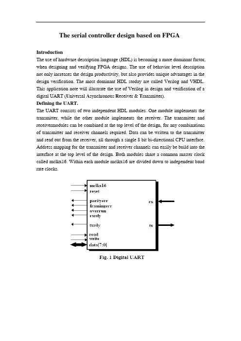
The serial controller design based on FPGAIntroductionThe use of hardware description language (HDL) is becoming a more dominant factor, when designing and verifying FPGA designs. The use of behavior level description not only increases the design productivity, but also provides unique advantages in the design verification. The most dominant HDL stoday are called Verilog and VHDL. This application note will illustrate the use of Verilog in design and verification of a digital UART (U niversal A synchronous R eceiver & T ransmitter).Defining the UART.The UART consists of two independent HDL modules. One module implements the transmitter, while the other module implements the receiver. The transmitter and receivermodules can be combined at the top level of the design, for any combinations of transmitter and receiver channels required. Data can be written to the transmitter and read out from the receiver, all through a single 8 bit bi-directional CPU interface. Address mapping for the transmitter and receiver channels can easily be build into the interface at the top level of the design. Both modules share a common master clock called mclkx16. Within each module mclkx16 are divided down to independent baud rate clocks.UART functional overview.A basic overview of the UART is shown below. At the left hand side is shown “transmit hold register”,“transmit shift register” and the transmitter “control logic” block, all contained within the transmitter module called “txmit”. At the right hand side is shown the “receive shift register”, “receive hold register”and the receiver “control logic” block, all contained within the receiver module called “rxcver”. The two modules have separate inputs and outputs for most of their control lines, only the bi-directional data bus, master clock and reset lines are shared by both modules.UART timing diagrams.Below is shown, how data written to the “transmit hold register” gets loaded into the “transmit shift register”, and at the rising edge of the baud rate clock, shifted to tx output.The Transmitter module.The master clock called mclkx16 are divided down to the proper baud rate called txclk and equals to mclkx16/16. Data written in parallel format to the module are latched internally, and shifted in serial format to the tx output at the frequency of the baud rate clock. Data shifted to the tx output follows the UART data format shown in fig. 6.Behavioral description of the transmitter.The transmitter waits for new data to be written to the module. When new data are written a transmit sequence is initialized. Data that was written in parallel to the module gets transmitted as serial data frames at the tx output. When no transmit sequence are in place, the tx output is held high.Implementation of the transmitter module.Internal signals in Verilog are declared as “wire” or “reg” data types. Signals of the “wire” type are used for continuos assignments, also called combinatorial statements. Signals of the “reg” type are used for assignments within the Verilog “always” block, often use for sequential logic assignments, but not necessarily. For further explanation see a Verilog reference book. Data types of the internal signals of the module can be referred to in table 3.We have now passed by all necessary declarations, and are now ready to look at the actual implementation. Using hardware description language allows us to describe the function of the transmitter in a more behavioral manner, rather than focus on it’s actual implementation at gate level.In software programming language, functions and procedures breaks larger programsinto more readable, manageable and certainly maintainable pieces.A Verilog function and task are used as the equivalent to multiple lines of Verilog code, where certain inputs or signals affects certain outputs or variables. The use of functions and tasks usually takes place where multiple lines of code are repeat edly used in a design, and hence makes the design easier to read and certainly maintain.A Verilog function can have multiple inputs, but always have only one output, while the Verilog task can have both multiple inputs, and multiple outputs. Below is shown the Verilog task, that hold all necessary seque ntial statements, to describe the transmitter in the “shift” mode.We here see the two tag bits called tag1 and tag2 concatenated to the “transmit shift register.Similar tasks were created to describe the transmitter in “idle” and “load”modes.By using these Verilog tasks, we can now create a very“ easy to read”behavioral model of the hole transmit process.If tx done and tx datardy both are true, the transmitter enter load mode. Next to the lo ad mode, the transmitter enters shift mode. At the rising edge of the baud rate clock, the contents of tsr are shifted to the tx output. Parity generation takes place during shifting of the tsr, as shown below.Simulation of a transmit sequenceThe contents of the data bus are latched into thr at the rising edge of write. At the next rising edge of txclk, the contents of thr are loaded into tsr, the active low start bit is a asserted to tx, and the txrdy flag indicates, that thr again is ready for new data to be written. At each rising edge of txclk, the contents of tsr is shifted to tx. Parity generati on takes place during shifting of data. Parity cycle is high one cycle next to last cycle, and tx gets the parity result.The Receiver module.The master clock mclkx16 are divided down to the proper baud rate clock called rxclk, and equals to mclkx16/16. Serial data to be received at the rx input of the module,mu st follow the UART data format. Data received in serial format can be read out inparallel format, through the 8 bit data bus.Behavioral description of the receiver.Between successive transmissions, the transmission line is held high, according to standard UART behavior. The receiver waits in “idle” mode for the rx input to go low. At the falling edge of rx the receiver enter “hunting” mode, now searching for a validstart bit of a new data frame to be received. If a valid start bit is detected, the receiver enter “shift data” mode. During receive of a data frame, various parity and error checks are performed. When a complete data frame has been received the receiver returns to idle mode. The basic operation of the receiver works as shown below.Implementation of the receiver module.In order to create an easy to read and easy to maintain behavioral model of the recei ver two Verilog tasks are written to describe the different modes of the receiver. The Verilog tas k called “idle_reset” holds all necessary sequential statements to describe the receiver at reset condition, and when the receiver is in it’s idle mode.When the receiver is not at it’s reset condition, and not in it’s idle mode, the receiver samples data at the rx input, shifts the data to the “receive shift register”, and generates parity based on the incoming data. The Verilog task called “shift_data” holds all necessary sequential statements to describe all above actions.Using the two Verilog tasks described above, we are now able to create the behavioral level description of the receiver at it’s reset condition, idle mode or when shifting in date . All above actions is synchronous to the baudrate clock called rxclk, and the im plementation is shown below.A complete data frame has been received, when the leading low start bit reaches rsr[0], and the receiver returns to idle mode again at the next rising edge of rxclk. At return to “idle” mode the receiver raises the “receive data ready” interrup t to indicate, that the new data received now can be read out in parallel format. Error flags are updated as well upon return to “idle” mode, and cleared when data are read out of the receiver. At the falling edge of read, the contents of the rhr are latched to the data bus. In table 8 shown below are the various error checks supported by the receiver.Simulation of a receive sequence.Between successive transmissions, the transmission line is held high. At the falling edge of rx input, the internal rxcnt starts counting up, synchronous to mclkx16. If rx input stays low for 8 cycles of mclkx16, the internal status bit idle is reset, and there by enable generation of rxclk. Rxclk is now synchronized to the center point of the l ow start bit. At the rising edge of rxclk, data are shifted from the rx input to rsr. When the leading low start bit reach rsr[0], the next rising edge of rxclk forces idle high aga in and there by disable generation of rxclk.At return to idle mode, the contents of rsr are loaded into rhr, the status flags are updated. The flag “rxrdy” now indicates, that the contents of rhr can be read out. At the falling edge of read, the contents of rhr are applied to the data bus.Using Hardware Description Language for Simulation.We have now studied how HDL can be used for the behavioral level design impleme ntation of a digital UART. While HDL make the design implementation easier to read and hopefully to understand as well, it also provides the ability to easily describe dep endency in between various processes that usually occur in such a complex event dri ven systems, as for example the UART. This ability to describe dependency in betwe en various processes is extremely need for simulation purposes as we will see very so on.Simulation stimulu s in Verilog HDL is called a “test fixture”. A test-fixture is a Verilog module that holds all lines of HDL code necessary to generate the simulation stimulus, while it at the same time port maps these signals to the design that are to be simulated. The port mapping is done by hierarchical module instantiation of the UAR T top level module into the test-fixture, as shown below.This allows simulation stimulus to be applied to the inputs of the design, while monit oring the outputs of the design. Input stimulus can be made conditionally to the response on the outputs ect. In fig. 19 shown below is illustrated, how the test-fixture port maps to the top level of the UART.Within the test-fixture the tx output of the transmitter module is looped back to the rx input of the receiver module. This allows the transmitter module to be used as test sig nal generator for the receiver module. Data can be written in parallel format to the tra nsmitter module and looped back in serial format to the rx input of the receiver modu al and data received can finally be read out in parallel format from the receiver modu al. In order to automate the testing of the UART as much as possible, tree independent Verilog tasks were written as follows. The Verilog task“write_to_transmitter” holds all necessary statements required to generate a single parallel data write sequence to the transmitter module. Data that are written to the transmitter upon execution of the “write_to_transmitter” task, get latched internal to the test-fixture for later analysis. The Verilog task “read_out_receiver” holds all necessary statements required to ge nerate a single parallel data read out sequence from the receiver module. Data that are read out of the receiver upon execution of the “read_out_receiver” task, get latchedinternal to the test-fixture for later analysis. The Verilog task “compare_data” holds all necessary statements required to compare the previous data written to the transmit ter module, to the corresponding and most recent data received and read out from the receiver module. If any discrepancy occurs, the “compare_data” task flags for an err or by writing out the data values that were written to the transmitter module, as well as the corresponding data values that were received by and read out from the receiver module.Silicon for synthesis.While HDL as design implementation method offers several advantages over traditio nal FPGA design entry approaches such as schematic capture, it meanwhile require great flexibility as well as high performance by the target devices for the synthesis flow. The synthesis flow for the UART has been targeted two flexible and high perfo rmance FPGA architectures available from QuickLogic, called the pASIC-1 and the pASIC-2 families.After synthesis, the design were placed & routed using the Place & Route tools from QuickLogic. After the Place & Route, the UART design were simulated using back-annotated Verilog post-layout timing models. The fast Verilog simulator called Silos III from Simucad were used for the post-layout simulation. All used tools are available within the QuickWorks tool suite from QuickLogic.基于FPGA的串口控制器设计简介使用硬件描述语言 (HDL) 设计和开发验证FPGA成为当前的主流因素。
w毕业设计论文外文资料翻译题目: Latest Development Trend Observation of FPGA FPGA 技术开展探究院系名称:信息科学与工程学院专业班级:电子信息科学与技术级2 班学生姓名:学号:指导教师:教师职称:副教授附件:1.外文资料翻译译文;2.外文原文。
指导教师评语:该生的英文资料与设计题目密切相关,中文翻译语句通顺,意思准确,字数符合要求,说明该生具有一定的阅读英文资料的能力。
签名:年月日w附件1:外文资料翻译译文FPGA 技术开展探究一.绪言自1985 年Xilinx 公司推出第一片现场可编程逻辑器件〔FPGA〕至今FPGA 已经历了十几年的开展历史。
在这十几年的开展过程中以FPGA 为代表的数字系统现场集成技术取得了惊人的开展:现场可编程逻辑器件从最初的1200 个可利用门开展到90 年代的25 万个可利用门乃至当新世纪来临之即国际上现场可编程逻辑器件的著名厂商Altera 公司、Xilinx 公司又陆续推出了数百万门的单片FPGA 芯片将现场可编程器件的集成度提高到一个新的水平。
纵观现场可编程逻辑器件的开展历史其之所以具有巨大的市场吸引力根本在于:FPGA 不仅可以解决电子系统小型化、低功耗、高可靠性等问题而且其开发周期短、开发软件投入少、芯片价格不断降低促使FPGA 越来越多地取代了ASIC 的市场特别是对小批量、多品种的产品需求使FPGA 成为首选。
目前FPGA 的主要开展动向是:随着大规模现场可编程逻辑器件的开展系统设计进入quot片上可编程系统quot〔SOPC〕的新纪元芯片朝着高密度、低压、低功耗方向挺进国际各大公司都在积极扩充其IP 库以优化的资源更好的满足用户的需求扩大市场特别是引人注目的所谓FPGA 动态可重构技术的开拓将推动数字系统设计观念的巨大转变。
二.Xilinx 公司研制开发的FPGA 系列产品的主要特征Xilinx 公司自创造FPGA 以来就不断的推出新器件和开发工具力求芯片的速度更高、功耗更低。
使用LabVIEW FPGA模块开发可编程自动化控制器Building Programmable Automation Controllers with LabVIEW FPGA OverviewProgrammable Automation Controllers (PACs) are gaining acceptance within the industrial control market as the ideal solution for applications that require highly integrated analog and digital I/O, floating-point processing, and seamless connectivity to multiple processing nodes. National Instruments offers a variety of PAC solutions powered by one common software development environment, NI LabVIEW. With LabVIEW, you can build custom I/O interfaces for industrial applications using add-on software, such as the NI LabVIEW FPGA Module.With the LabVIEW FPGA Module and reconfigurable I/O (RIO) hardware, National Instruments delivers an intuitive, accessible solution for incorporating the flexibility and customizability of FPGA technology into industrial PAC systems. You can define the logic embedded in FPGA chips across the family of RIO hardware targets without knowing low-level hardware description languages (HDLs) or board-level hardware design details, as well as quickly define hardware for ultrahigh-speed control, customized timing and synchronization, low-level signal processing, and custom I/O with analog, digital, and counters within a single device. Youalso can integrate your custom NI RIO hardware with image acquisition and analysis, motion control, and industrial protocols, such as CAN and RS232, to rapidly prototype and implement a complete PAC system.Table of Contents1.Introduction2.NI RIO Hardware for PACs3.Building PACs with LabVIEW and the LabVIEW FPGA Module4.FPGA Development Flowing NI SoftMotion to Create Custom Motion Controllers6.Applications7.ConclusionIntroductionYou can use graphical programming in LabVIEW and the LabVIEW FPGA Module to configure the FPGA (field-programmable gate array) on NI RIO devices. RIO technology, the merging of LabVIEW graphical programming with FPGAs on NI RIO hardware, provides a flexible platform for creating sophisticated measurement and control systems that you could previously create only with custom-designed hardware.An FPGA is a chip that consists of many unconfigured logic gates. Unlike the fixed, vendor-defined functionality of an ASIC(application-specific integrated circuit) chip, you can configure and reconfigure the logic on FPGAs for your specific application. FPGAs are used in applications where either the cost of developing and fabricating an ASIC is prohibitive, or the hardware must be reconfigured after being placed into service. The flexible, software-programmable architecture of FPGAs offer benefits such as high-performance execution of custom algorithms, precise timing and synchronization, rapid decision making, and simultaneous execution of parallel tasks. Today, FPGAs appear in such devices as instruments, consumer electronics, automobiles, aircraft, copy machines, and application-specific computer hardware. While FPGAs are often used in industrial control products, FPGA functionality has not previously been made accessible to industrial control engineers. Defining FPGAs has historically required expertise using HDL programming or complex design tools used more by hardware design engineers than by control engineers.With the LabVIEW FPGA Module and NI RIO hardware, you now can use LabVIEW, a high-level graphical development environment designed specifically for measurement and control applications, to create PACs that have the customization, flexibility, and high-performance of FPGAs. Because the LabVIEW FPGA Module configures custom circuitry in hardware, your system can process and generate synchronized analog and digitalsignals rapidly and deterministically. Figure 1 illustrates many of the NI RIO devices that you can configure using the LabVIEW FPGA Module.Figure 1. LabVIEW FPGA VI Block Diagram and RIO Hardware Platforms NI RIO Hardware for PACsHistorically, programming FPGAs has been limited to engineers who have in-depth knowledge of VHDL or other low-level design tools, which require overcoming a very steep learning curve. With the LabVIEW FPGA Module, NI has opened FPGA technology to a broader set of engineers who can now define FPGA logic using LabVIEW graphical development. Measurement and control engineers can focus primarily on their test and control application, where their expertise lies, rather than the low-level semantics of transferring logic into the cells of the chip. The LabVIEW FPGA Module model works because of the tight integration between the LabVIEW FPGA Module and the commercial off-the-shelf (COTS) hardware architecture of the FPGA and surrounding I/O components.National Instruments PACs provide modular, off-the-shelf platforms for your industrial control applications. With the implementation of RIO technology on PCI, PXI, and Compact Vision System platforms and the introduction of RIO-based CompactRIO, engineers now have the benefits of a COTS platform with the high-performance, flexibility, and customizationbenefits of FPGAs at their disposal to build PACs. National Instruments PCI and PXI R Series plug-in devices provide analog and digital data acquisition and control for high-performance, user-configurable timing and synchronization, as well as onboard decision making on a single device. Using these off-the-shelf devices, you can extend your NI PXI or PCI industrial control system to include high-speed discrete and analog control, custom sensor interfaces, and precise timing and control.NI CompactRIO, a platform centered on RIO technology, provides a small, industrially rugged, modular PAC platform that gives you high-performance I/O and unprecedented flexibility in system timing. You can use NI CompactRIO to build an embedded system for applications such as in-vehicle data acquisition, mobile NVH testing, and embedded machine control systems. The rugged NI CompactRIO system is industrially rated and certified, and it is designed for greater than 50 g of shock at a temperature range of -40 to 70 °C.NI Compact Vision System is a rugged machine vision package that withstands the harsh environments common in robotics, automated test, and industrial inspection systems. NI CVS-145x devices offer unprecedented I/O capabilities and network connectivity for distributed machine vision applications.NI CVS-145x systems use IEEE 1394 (FireWire) technology, compatible with more than 40 cameras with a wide range of functionality,performance, and price. NI CVS-1455 and NI CVS-1456 devices contain configurable FPGAs so you can implement custom counters, timing, or motor control in your machine vision application.Building PACs with LabVIEW and the LabVIEW FPGA ModuleWith LabVIEW and the LabVIEW FPGA Module, you add significant flexibility and customization to your industrial control hardware. Because many PACs are already programmed using LabVIEW, programming FPGAs with LabVIEW is easy because it uses the same LabVIEW development environment. When you target the FPGA on an NI RIO device, LabVIEW displays only the functions that can be implemented in the FPGA, further easing the use of LabVIEW to program FPGAs. The LabVIEW FPGA Module Functions palette includes typical LabVIEW structures and functions, such as While Loops, For Loops, Case Structures, and Sequence Structures as well as a dedicated set of LabVIEW FPGA-specific functions for math, signal generation and analysis, linear and nonlinear control, comparison logic, array and cluster manipulation, occurrences, analog and digital I/O, and timing. You can use a combination of these functions to define logic and embed intelligence onto your NI RIO device.Figure 2 shows an FPGA application that implements a PID control algorithm on the NI RIO hardware and a host application on a Windows machine or an RT target that communicates with the NI RIO hardware. Thisapplication reads from analog input 0 (AI0), performs the PID calculation, and outputs the resulting data on analog output 0 (AO0). While the FPGA clock runs at 40 MHz the loop in this example runs much slower because each component takes longer than one-clock cycle to execute. Analog control loops can run on an FPGA at a rate of about 200 kHz. You can specify the clock rate at compile time. This example shows only one PID loop; however, creating additional functionality on the NI RIO device is merely a matter of adding another While Loop. Unlike traditional PC processors, FPGAs are parallel processors. Adding additional loops to your application does not affect the performance of your PID loop.Figure 2. PID Control Using an Embedded LabVIEW FPGA VI withCorresponding LabVIEW Host VI.FPGA Development FlowAfter you create the LabVIEW FPGA VI, you compile the code to run on the NI RIO hardware. Depending on the complexity of your code and the specifications of your development system, compile time for an FPGA VI can range from minutes to several hours. To maximize development productivity, with the R Series RIO devices you can use a bit-accurate emulation mode so you can verify the logic of your design before initiating the compile process. When you target the FPGA Device Emulator, LabVIEW accesses I/O from the device and executes the VI logic on the Windowsdevelopment computer. In this mode, you can use the same debugging tools available in LabVIEW for Windows, such as execution highlighting, probes, and breakpoints.Once the LabVIEW FPGA code is compiled, you create a LabVIEW host VI to integrate your NI RIO hardware into the rest of your PAC system. Figure 3 illustrates the development process for creating an FPGA application. The host VI uses controls and indicators on the FPGA VI front panel to transfer data between the FPGA on the RIO device and the host processing engine. These front panel objects are represented as data registers within the FPGA. The host computer can be either a PC or PXI controller running Windows or a PC, PXI controller, Compact Vision System, or CompactRIO controller running a real-time operating system (RTOS). In the above example, we exchange the set point, PID gains, loop rate, AI0, and AO0 data with the LabVIEW host VI.Figure 3. LabVIEW FPGA Development FlowThe NI RIO device driver includes a set of functions to develop a communication interface to the FPGA. The first step in building a host VI is to open a reference to the FPGA VI and RIO device. The Open FPGA VI Reference function, as seen in Figure 2, also downloads and runs the compiled FPGA code during execution. After opening the reference, you read and write to the control and indicator registers on the FPGA using theRead/Write Control function. Once you wire the FPGA reference into this function, you can simply select which controls and indicators you want to read and write to. You can enclose the FPGA Read/Write function within a While Loop to continuously read and write to the FPGA. Finally, the last function within the LabVIEW host VI in Figure 2 is the Close FPGA VI Reference function. The Close FPGA VI Reference function stops the FPGA VI and closes the reference to the device. Now you can download other compiled FPGA VIs to the device to change or modify its functionality.The LabVIEW host VI can also be used to perform floating-point calculations, data logging, networking, and any calculations that do not fit within the FPGA fabric. For added determinism and reliability, you can run your host application on an RTOS with the LabVIEW Real-Time Module. LabVIEW Real-Time systems provide deterministic processing engines for functions performed synchronously or asynchronously to the FPGA. For example, floating-point arithmetic, including FFTs, PID calculations, and custom control algorithms, are often performed in the LabVIEW Real-Time environment. Relevant data can be stored on a LabVIEW Real-Time system or transferred to a Windows host computer for off-line analysis, data logging, or user interface displays. The architecture for this configuration is shown in Figure 4. Each NI PAC platform that offers RIO hardware can run LabVIEW Real-Time VIs.Figure 4. Complete PAC Architecture Using LabVIEW FPGA, LabVIEW Real-Timeand Host PCWithin each R Series and CompactRIO device, there is flash memory available to store a compiled LabVIEW FPGA VI and run the application immediately upon power up of the device. In this configuration, as long as the FPGA has power, it runs the FPGA VI, even if the host computer crashes or is powered down. This is ideal for programming safety power down and power up sequences when unexpected events occur.Using NI SoftMotion to Create Custom Motion ControllersThe NI SoftMotion Development Module for LabVIEW provides VIs and functions to help you build custom motion controllers as part of NI PAC hardware platforms that can include NI RIO devices, DAQ devices, and Compact FieldPoint. NI SoftMotion provides all of the functions that typically reside on a motion controller DSP. With it, you can handle path planning, trajectory generation, and position and velocity loop control in the NI LabVIEW environment and then deploy the code on LabVIEW Real-Time or LabVIEW FPGA-based target hardware.NI SoftMotion includes functions for trajectory generator and spline engine and examples with complete source code for supervisory control, position, and velocity control loop using the PID algorithm. Supervisory control and the trajectory generator run on a LabVIEW Real-Time target and run at millisecond loop rates. The spline engine and the control loop can run either on a LabVIEW Real-Time target at millisecond loop rates or on a LabVIEW FPGA target at microsecond loop rates.ApplicationsBecause the LabVIEW FPGA Module can configure low-level hardware design of FPGAs and use the FPGAs within in a modular system, it is ideal for industrial control applications requiring custom hardware. These custom applications can include a custom mix of analog, digital, and counter/timer I/O, analog control up to 125 kHz, digital control up to 20 MHz, and interfacing to custom digital protocols for the following:•Batch control•Discrete control•Motion control•In-vehicle data acquisition•Machine condition monitoring•Rapid control prototyping (RCP)•Industrial control and acquisition•Distributed data acquisition and control•Mobile/portable noise, vibration, and harshness (NVH) analysisConclusionThe LabVIEW FPGA Module brings the flexibility, performance, and customization of FPGAs to PAC platforms. Using NI RIO devices and LabVIEW graphical programming, you can build flexible and custom hardware using the COTS hardware often required in industrial control applications. Because you are using LabVIEW, a programming language already used in many industrial control applications, to define your NI RIO hardware, there is no need to learn VHDL or other low-level hardware design tools to create custom hardware. Using the LabVIEW FPGA Module and NI RIO hardware as part of your NI PAC adds significant flexibility and functionality for applications requiring ultrahigh-speed control, interfaces to custom digital protocols, or a custom I/O mix of analog, digital, and counters.使用LabVIEW FPGA(现场可编程门阵列)模块开发可编程自动化控制器综述工业控制上的应用要求高度集成的模拟和数字输入输出、浮点运算和多重处理节点的无缝连接。
Building Programmable Automation Controllers with LabVIEWFPGAOverviewProgrammable Automation Controllers (PACs) are gaining acceptance within the industrial control market as the ideal solution for applications that require highly integrated analog and digital I/O, floating-point processing, and seamless connectivity to multiple processing nodes. National Instruments offers a variety of PAC solutions powered by one common software development environment, NI LabVIEW. With LabVIEW, you can build custom I/O interfaces for industrial applications using add-on software, such as the NI LabVIEW FPGA Module.With the LabVIEW FPGA Module and reconfigurable I/O (RIO) hardware, National Instruments delivers an intuitive, accessible solution for incorporating the flexibility and customizability of FPGA technology into industrial PAC systems. You can define the logic embedded in FPGA chips across the family of RIO hardware targets without knowing low-level hardware description languages (HDLs) or board-level hardware design details, as well as quickly define hardware for ultrahigh-speed control, customized timing and synchronization, low-level signal processing, and custom I/O with analog, digital, and counters within a single device. You also can integrate your custom NI RIO hardware with image acquisition and analysis, motion control, and industrial protocols, such as CAN and RS232, to rapidly prototype and implement a complete PAC system.Table of Contents1.Introduction2.NI RIO Hardware for PACs3.Building PACs with LabVIEW and the LabVIEW FPGA Module4.FPGA Development Flowing NI SoftMotion to Create Custom Motion Controllers6.Applications7.ConclusionIntroductionYou can use graphical programming in LabVIEW and the LabVIEW FPGA Module to configure the FPGA (field-programmable gate array) on NI RIO devices. RIO technology, the merging of LabVIEW graphical programming with FPGAs on NI RIO hardware, provides a flexible platform for creating sophisticated measurement and control systems that you could previously create only with custom-designed hardware.An FPGA is a chip that consists of many unconfigured logic gates. Unlike the fixed, vendor-defined functionality of an ASIC (application-specific integrated circuit) chip, you can configure and reconfigure the logic on FPGAs for your specific application. FPGAs are used in applications where either the cost of developing and fabricating an ASIC is prohibitive, or the hardware must be reconfigured after being placed into service. The flexible,software-programmable architecture of FPGAs offer benefits such as high-performance execution of custom algorithms, precise timing and synchronization, rapid decision making, and simultaneous execution of parallel tasks. Today, FPGAs appear in such devices as instruments, consumer electronics, automobiles, aircraft, copy machines, andapplication-specific computer hardware. While FPGAs are often used in industrial control products, FPGA functionality has not previously been made accessible to industrial control engineers. Defining FPGAs has historically required expertise using HDL programming or complex design tools used more by hardware design engineers than by control engineers.With the LabVIEW FPGA Module and NI RIO hardware, you now can use LabVIEW, a high-level graphical development environment designed specifically for measurement and control applications, to create PACs that have the customization, flexibility, andhigh-performance of FPGAs. Because the LabVIEW FPGA Module configures custom circuitry in hardware, your system can process and generate synchronized analog and digital signals rapidly and deterministically. Figure 1 illustrates many of the NI RIO devices that you can configure using the LabVIEW FPGA Module.Figure 1. LabVIEW FPGA VI Block Diagram and RIO Hardware PlatformsNI RIO Hardware for PACsHistorically, programming FPGAs has been limited to engineers who have in-depth knowledge of VHDL or other low-level design tools, which require overcoming a very steep learning curve. With the LabVIEW FPGA Module, NI has opened FPGA technology to a broader set of engineers who can now define FPGA logic using LabVIEW graphical development. Measurement and control engineers can focus primarily on their test and control application, where their expertise lies, rather than the low-level semantics of transferring logic into the cells of the chip. The LabVIEW FPGA Module model works because of the tightintegration between the LabVIEW FPGA Module and the commercial off-the-shelf (COTS) hardware architecture of the FPGA and surrounding I/O components.National Instruments PACs provide modular, off-the-shelf platforms for your industrial control applications. With the implementation of RIO technology on PCI, PXI, and Compact Vision System platforms and the introduction of RIO-based CompactRIO, engineers now have the benefits of a COTS platform with the high-performance, flexibility, and customization benefits of FPGAs at their disposal to build PACs. National Instruments PCI and PXI R Series plug-in devices provide analog and digital data acquisition and control for high-performance, user-configurable timing and synchronization, as well as onboard decision making on a single device. Using these off-the-shelf devices, you can extend your NI PXI or PCI industrial control system to include high-speed discrete and analog control, custom sensor interfaces, and precise timing and control.NI CompactRIO, a platform centered on RIO technology, provides a small, industrially rugged, modular PAC platform that gives you high-performance I/O and unprecedented flexibility in system timing. You can use NI CompactRIO to build an embedded system for applications such as in-vehicle data acquisition, mobile NVH testing, and embedded machine control systems. The rugged NI CompactRIO system is industrially rated and certified, and it is designed for greater than 50 g of shock at a temperature range of -40 to 70 °C.NI Compact Vision System is a rugged machine vision package that withstands the harsh environments common in robotics, automated test, and industrial inspection systems. NICVS-145x devices offer unprecedented I/O capabilities and network connectivity for distributed machine vision applications.NI CVS-145x systems use IEEE 1394 (FireWire) technology, compatible with more than 40 cameras with a wide range of functionality, performance, and price. NI CVS-1455 and NI CVS-1456 devices contain configurable FPGAs so you can implement custom counters, timing, or motor control in your machine vision application.Building PACs with LabVIEW and the LabVIEW FPGA Module With LabVIEW and the LabVIEW FPGA Module, you add significant flexibility and customization to your industrial control hardware. Because many PACs are already programmed using LabVIEW, programming FPGAs with LabVIEW is easy because it uses the same LabVIEW development environment. When you target the FPGA on an NI RIO device, LabVIEW displays only the functions that can be implemented in the FPGA, further easing the use of LabVIEW to program FPGAs. The LabVIEW FPGA Module Functions palette includes typical LabVIEW structures and functions, such as While Loops, For Loops, Case Structures, and Sequence Structures as well as a dedicated set of LabVIEWFPGA-specific functions for math, signal generation and analysis, linear and nonlinear control, comparison logic, array and cluster manipulation, occurrences, analog and digital I/O, and timing. You can use a combination of these functions to define logic and embed intelligence onto your NI RIO device.Figure 2 shows an FPGA application that implements a PID control algorithm on the NI RIO hardware and a host application on a Windows machine or an RT target that communicates with the NI RIO hardware. This application reads from analog input 0 (AI0), performs the PID calculation, and outputs the resulting data on analog output 0 (AO0). While the FPGA clock runs at 40 MHz the loop in this example runs much slower because each component takes longer than one-clock cycle to execute. Analog control loops can run on an FPGA at a rate of about 200 kHz. You can specify the clock rate at compile time. This example shows only one PID loop; however, creating additional functionality on the NI RIO device is merely a matter of adding another While Loop. Unlike traditional PC processors, FPGAs are parallel processors. Adding additional loops to your application does not affect the performance of your PID loop.Figure 2. PID Control Using an Embedded LabVIEW FPGA VI with Corresponding LabVIEW HostVI.FPGA Development FlowAfter you create the LabVIEW FPGA VI, you compile the code to run on the NI RIO hardware. Depending on the complexity of your code and the specifications of your development system, compile time for an FPGA VI can range from minutes to several hours.To maximize development productivity, with the R Series RIO devices you can use abit-accurate emulation mode so you can verify the logic of your design before initiating the compile process. When you target the FPGA Device Emulator, LabVIEW accesses I/O from the device and executes the VI logic on the Windows development computer. In this mode, you can use the same debugging tools available in LabVIEW for Windows, such as execution highlighting, probes, and breakpoints.Once the LabVIEW FPGA code is compiled, you create a LabVIEW host VI to integrate your NI RIO hardware into the rest of your PAC system. Figure 3 illustrates the development process for creating an FPGA application. The host VI uses controls and indicators on the FPGA VI front panel to transfer data between the FPGA on the RIO device and the host processing engine. These front panel objects are represented as data registers within the FPGA. The host computer can be either a PC or PXI controller running Windows or a PC, PXI controller, Compact Vision System, or CompactRIO controller running a real-time operating system (RTOS). In the above example, we exchange the set point, PID gains, loop rate, AI0, and AO0 data with the LabVIEW host VI.Figure 3. LabVIEW FPGA Development FlowThe NI RIO device driver includes a set of functions to develop a communication interface to the FPGA. The first step in building a host VI is to open a reference to the FPGA VI and RIO device. The Open FPGA VI Reference function, as seen in Figure 2, also downloads and runs the compiled FPGA code during execution. After opening the reference, you read and write to the control and indicator registers on the FPGA using the Read/Write Control function. Once you wire the FPGA reference into this function, you can simply select which controls and indicators you want to read and write to. You can enclose the FPGA Read/Write function within a While Loop to continuously read and write to the FPGA. Finally, the last function within the LabVIEW host VI in Figure 2 is the Close FPGA VI Reference function. The Close FPGA VI Reference function stops the FPGA VI and closes the reference to the device. Now you can download other compiled FPGA VIs to the device to change or modify its functionality.The LabVIEW host VI can also be used to perform floating-point calculations, data logging, networking, and any calculations that do not fit within the FPGA fabric. For added determinism and reliability, you can run your host application on an RTOS with the LabVIEW Real-Time Module. LabVIEW Real-Time systems provide deterministicprocessing engines for functions performed synchronously or asynchronously to the FPGA. For example, floating-point arithmetic, including FFTs, PID calculations, and custom control algorithms, are often performed in the LabVIEW Real-Time environment. Relevant data can be stored on a LabVIEW Real-Time system or transferred to a Windows host computer for off-line analysis, data logging, or user interface displays. The architecture for this configuration is shown in Figure 4. Each NI PAC platform that offers RIO hardware can run LabVIEW Real-Time VIs.Figure 4. Complete PAC Architecture Using LabVIEW FPGA, LabVIEW Real-Time and Host PC Within each R Series and CompactRIO device, there is flash memory available to store a compiled LabVIEW FPGA VI and run the application immediately upon power up of the device. In this configuration, as long as the FPGA has power, it runs the FPGA VI, even if the host computer crashes or is powered down. This is ideal for programming safety power down and power up sequences when unexpected events occur.Using NI SoftMotion to Create Custom Motion ControllersThe NI SoftMotion Development Module for LabVIEW provides VIs and functions to help you build custom motion controllers as part of NI PAC hardware platforms that can include NI RIO devices, DAQ devices, and Compact FieldPoint. NI SoftMotion provides all of the functions that typically reside on a motion controller DSP. With it, you can handle path planning, trajectory generation, and position and velocity loop control in the NI LabVIEW environment and then deploy the code on LabVIEW Real-Time or LabVIEW FPGA-based target hardware.NI SoftMotion includes functions for trajectory generator and spline engine and examples with complete source code for supervisory control, position, and velocity control loop using the PID algorithm. Supervisory control and the trajectory generator run on a LabVIEW Real-Time target and run at millisecond loop rates. The spline engine and the control loop can run either on a LabVIEW Real-Time target at millisecond loop rates or on a LabVIEW FPGA target at microsecond loop rates.ApplicationsBecause the LabVIEW FPGA Module can configure low-level hardware design of FPGAs and use the FPGAs within in a modular system, it is ideal for industrial controlapplications requiring custom hardware. These custom applications can include a custom mix of analog, digital, and counter/timer I/O, analog control up to 125 kHz, digital control up to 20 MHz, and interfacing to custom digital protocols for the following:•Batch control•Discrete control•Motion control•In-vehicle data acquisition•Machine condition monitoring•Rapid control prototyping (RCP)•Industrial control and acquisition•Distributed data acquisition and control•Mobile/portable noise, vibration, and harshness (NVH) analysis ConclusionThe LabVIEW FPGA Module brings the flexibility, performance, and customization of FPGAs to PAC platforms. Using NI RIO devices and LabVIEW graphical programming, you can build flexible and custom hardware using the COTS hardware often required in industrial control applications. Because you are using LabVIEW, a programming language already used in many industrial control applications, to define your NI RIO hardware, there is no need to learn VHDL or other low-level hardware design tools to create custom hardware. Using the LabVIEW FPGA Module and NI RIO hardware as part of your NI PAC adds significant flexibility and functionality for applications requiring ultrahigh-speed control, interfaces to custom digital protocols, or a custom I/O mix of analog, digital, and counters.使用LabVIEW FPGA(现场可编程门阵列)模块开发可编程自动化控制器综述工业控制上的应用要求高度集成的模拟和数字输入输出、浮点运算和多重处理节点的无缝连接。