0.4 mw wideband lna with double gm enhancement and feed-forward noise cancellation
- 格式:pdf
- 大小:400.54 KB
- 文档页数:2
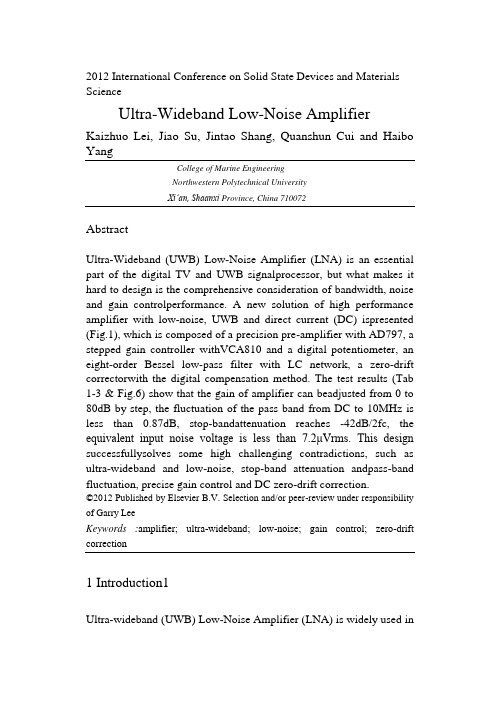
2012 International Conference on Solid State Devices and Materials ScienceUltra-Wideband Low-Noise Amplifier Kaizhuo Lei, Jiao Su, Jintao Shang, Quanshun Cui and Haibo YangCollege of Marine EngineeringNorthwestern Polytechnical UniversityXi’an, Shaanxi Province, China 710072AbstractUltra-Wideband (UWB) Low-Noise Amplifier (LNA) is an essential part of the digital TV and UWB signalprocessor, but what makes it hard to design is the comprehensive consideration of bandwidth, noise and gain controlperformance. A new solution of high performance amplifier with low-noise, UWB and direct current (DC) ispresented (Fig.1), which is composed of a precision pre-amplifier with AD797, a stepped gain controller withVCA810 and a digital potentiometer, an eight-order Bessel low-pass filter with LC network, a zero-drift correctorwith the digital compensation method. The test results (Tab 1-3 & Fig.6) show that the gain of amplifier can beadjusted from 0 to 80dB by step, the fluctuation of the pass band from DC to 10MHz is less than 0.87dB, stop-bandattenuation reaches -42dB/2fc, the equivalent input noise voltage is less than 7.2μVrms. This design successfullysolves some high challenging contradictions, such as ultra-wideband and low-noise, stop-band attenuation andpass-band fluctuation, precise gain control and DC zero-drift correction.©2012 Published by Elsevier B.V. Selection and/or peer-review under responsibility of Garry LeeKeywords :amplifier; ultra-wideband; low-noise; gain control; zero-drift correction1 Introduction1Ultra-wideband (UWB) Low-Noise Amplifier (LNA) is widely used inthe mid-frequency and videoamplifiers. This kind of circuit is not only used to amplify the video signal, impulse signal and RF signalwith the bandwidth ranging from DC to several MHz or even tens of MHz [1], but also widely applied inthe signal processing [2]. In recent years, with the rapid development of ultra-wideband in the covertcommunication [3] and target detection [4], higher requirements for the bandwidth are claimed by theUWB signal, thus the front-end preprocessing circuit of the receiver must be a low-noise amplifier [5][6] with UWB [7]-[9].The performance [10] of the ultra-wideband amplifier directly influences the precision of signaldetection and processing. As a consequence, the design of low-noise, low zero-drift and ultra-widebandbecomes the key point which is of great engineering significance and application value [11]. In other references, the typical gain of UWB LNA was 12-20dB [12] and there was also a contradiction between performance and feasibility. For example, Ref.[13] [14] proposed the amplifier which solved the problem of ultra-wideband and low-noise but it couldn’t avoid zero-drift and high NF.This paper designed and realized a low-noise wideband amplifier made up with the low-noise amplifier, high performance filter network [15], and digital program control circuit for zero-drift correction [16], MCU control system and high precision power supply. Several contradictions such as the ultra-wideband and low-noise, the high stop-band attenuation and low pass-band fluctuation, the high precise gain control and the compensation of DC zero-drift, etc. were successfully solved [17]. The design of our machine got superior parameters and reliable performance together with better promotion value.2 Solution Of Low-Noise And Ultra-widebandThe functional block diagram of the low-noise wideband DC amplifier is shown in Fig. 1. Theamplifier system contains five parts: the primary amplifier, filter network, zero-drift correction circuit,control system and high performance power supply. The primary amplifier consists of low-noise precise pre-amplifier, gain control, mid-amplifier and power driver circuit outputted by the final push-pull. Thelow-noise precise pre-amplifier adopts the ultra low-noise integrated operational chips, realizing the low-noise for the whole system. Voltage gain is adjusted by the MCU. Mid-amplifier consists of the low-noise, high speed integrated amplifier in order to increase the system gain. Final end power driver adopts the dual op-amp consisting of the pull-push output to increase the loading ability of the system. The high performance filter adopts the passive filter proposal to realize the 0~5MHz and 0~10MHz dual channel, eight-order Bessel low-pass filter with the switchable wave band. The zero-drift correction hastwo proposals: analog revised and digital revised, and here we adopt the digital one to increase the correction precision. The control system is to realize the gain and zero-drift digital control with the MCU AT89C52 [18] as the centre. Power supply adopts the mixed regulator, through the decoupling filter, secondary regulator and precise regulator in order to provide the precise low-noise DC power for the whole system.3 Design Of Circuits And Calculation Of Parameters3.1 The design of low-noise and ultra-widebandDecreasing the output noise is the key to the wideband amplifier. By using the Friis Formula we can get the noise coefficients of the cascade amplifier [19]:Where NF1、NF2…NFn are the noise coefficients of each amplifier, and Kpa1、Kpa2…Kpa(n-1) are the gains of each amplifier. From the Friis Formula we can see what affects the cascade amplifier most is the first stage amplifier, so we should try to get an amplifier of smaller noise coefficient and larger gain in the low-noise design.The design chooses the ultra low-noise integrated op-amp AD797 as the pre-amplifier matching the appropriate source impedance. The peripheral devices consist of high performance low-noise metal film resistors and each stage adopts low-noise chips. The LC low-pass filter with bands of 0~5MHz and 0~10MHz is designed. And also the analog and digital grounds are separated in the PCB layout and masking technique is also adopted in the preceding stage in order to decrease the output noise voltage. The low-noise pre-amplifierconsisting of AD797 is shown in Fig. 2.3.2 Program gain controlGain controller is a kind of control method with the amplifier gain changing along with the external control signal. In this system, the program gain control is realized easily by using the external keyboard to set the gain, the voltage gain control amplifier VCA 810 is selected as gain controller.With the control of MCU, the digital potentiometer X9C103 adjust the output voltage ranging between 0~2V, which is added to the VCA810 gain control pin. In this way, we can reach the system with the gain of 0~80dB and the 1dB step adjustable. The principle circuit of gain controller is shown in Fig. 3.3.3 DC zero-drift correctionDC zero-drift is that the operating point of DC amplifier irregularly, slowly and gradually changes.The greater the gain and the more magnification series, the more serious the phenomenon will be, even making the op-amp work badly when the zero-drift reaches the saturation. So a DC zero-drift correction circuit must be designed in order to guarantee the stability of DC amplifier. Through A/D sampling, the DC zero-drift detected in the final stage is sent into the MCU, then we can realize the automatic set of zero by choosing the proper reference voltage and using MCU to control digital potentiometer X9C102 with a compensation voltage adding to the zero regulating end. The zero-drift correction circuit is shown in Fig. 4.3.4 High performance filter networkThe filter is mainly used to reduce the noise, filter band interference and improve system stability. In this design, two low-pass filter pass-bands are 0..5MH and 0..10MHz, with the additional requirements of the pass-band fluctuation less than 1 dB, and stop-band attenuation 40dB/2fC, so precise capacitance and inductance are used to achieve the eight-order passive LC low-pass filter. In order to realize the linear phase, the Bessel filter has to be adopted. As for the complicated calculation and hardship in setting the parameters of LC filter, we can use the software named Filtering Solutions to do some computer aided design. The high performance filter is shown in Fig. 5.4 System performance test4.1 The measurement of the system’s self-noiseThe system is plugged in ±15V DC power supply with the input shorted to GND. The amplifier gain was adjusted to Av=40dB、60dB、80dB. The oscilloscope was used to observe the output noise waveforms of each amplifier and the Agilent 34401A was used to measure the RMS of noise voltage, the measure results are shown in TABLE I.4.2 The test of zero-drift correctionKeeping the input shorted and use the MCU to control the digital potentiometer, adding the compensation voltage by a step of 20 dB, adjusting the gain of amplifier in order to suppress the DCzero-drift .Use Agilent 34401A to measure the correction voltage under different magnifications, the results are shown in TABLE II.4.3 The calibration of the gainSet the working frequency band at 0~10MHz and the input signal frequency fi = 2MHz. Respectively,set the gain of amplifier separately at 0、20dB、40dB、60dB、80dB and input the appropriate signal amplitude Vi, use dual-channel oscilloscope to observe the input and output, record the output signal amplitude, calculate amplifier real gain and make comparisons with the set, the results are shown in TABLE III.4.4 Amplitude-frequency characteristics of the systemFix the amplitude of the input signal Vi = 100mVpp, AV=40dB, adjust the signal frequency between0~20MHz, then use the oscilloscope to observe VPP of the output signals with different frequency input signals and record them. Draw the curve of amplitude-frequency characteristic with MATLAB [20],which is shown in Fig.6.5 ConclusionIn this paper, the key technology of the ultra-wideband low-noise DC amplifier was researched. A high performance amplifier based on ultra-low-noise pre-amplifier, LC filter network, digital program gain control and zero-drift correction circuit was presented. The D/A converter was adopted to control the low-noise wideband amplifier VCA810, and the dynamic voltage gain range 0~80dB was achieved, the linear phase low-noise filter with band 0~10MHz was realized with the passive wideband Bessel low-pass filter, which composed by the inductance and capacitance, matched up with the low-noise preamplifier AD797, the equivalent input noise less than 7.2 μVrms was guaranteed. The MCU was used to control the digital potentiometer X9C102 to add compensation voltage to the zero-set end in order to realize the auto-adjustment of DC zero-drift. The test results show that the amplifier designed works with low-noise, small offset, high cost-effective, great stability and reliability.6 AcknowledgmentThe authors would like to thank Tiande Gao and Linwei Tao for help in the experiment, Zengxiang Fu and Hai Huang for advice in English writing.。

DATA SHEETHeadend Optics Platform (CH3000)HT3540H SeriesDouble-Density Full Spectrum DWDM Transmitter SystemThe CommScope HT3540H Series Double ‐Density Full Spectrum Dense Wave Division Multiplexing (DWDM) Transmitter System provides high performance and a high rack density forward path transmission solution for Cable TV service providers.The high ‐density packaging design allows up to four (4) HT3540H series high performance transmitters plus a CC3008 Communications Control Module to be stacked vertically and contained by the CA3008 module carrier, requiring only two chassis slots of a 3RU chassis. The compact solution supports up to 24 transmitters in a CH3000 chassis, including redundant power supplies.•Available in 40 wavelengths on ITU 100 GHz grid •Hot plug ‐in/out, individually replaceable transmitter modules•Optimized for full spectrum loading•Analog loading up to 552 MHz plus QAM loading •Manual or Automatic Gain Control (AGC) modes •Low power consumption•High rack density: 24 transmitters per 3RU chassis, with redundant power supplies and optical multiplexing•Front panel ‐20 dB input test point •Front panel laser On/Off switch•Local and remote status monitoring featuresFEATURESWhen installed in the chassis, the transmitters interface to a “zero ‐slot” back plate, providing support for up to four HT3540H series transmitters. The figure below shows a fully loaded carrier mated to the BD35M4 Double ‐Density multiplexing back plate that supports optical combining of four DWDM wavelengths in the forward path.The CC3008 Communications Module installed at the top of a HT3540H series transmitter stack provides the communications interface between the transmitters and the CH3000 mid ‐plane bus, allowing complete configuration and management control of the stack, both local andremote.HT3540H Series Quad ‐Stack and CC3008 Communications Module joined with a BD35M4 Multiplexing Back PlateHT3540H Series Double Density Full Spectrum DWDM Transmitters (1.2 GHz Passband)CommScope HT3540H Series Double‐Density Full Spectrum DWDM Transmitters are a key element of the CommScope HFC and Fiber Deep architectures in support of the evolution to all QAM transmission. These high‐performance transmitters are designed for Dense Wave Division Multiplexing (DWDM) applications for point‐to‐point forward path transmission of full spectrum broadcast and narrowcast services.HT3541H series transmitters are designed for “light” analog channel loading from 0 to 30 analog channels (up to 258 MHz) plus QAM channel loading, or for all QAM loading. They are also designed for QAM‐only loading for digital services as part of a BC/NC overlay system.HT3542H series transmitters are designed for “full” analog channel loading from 0 to 79 analog channels (up to 552 MHz) plus QAM channel loading.HT3543H series transmitters are designed for all QAM loading.These transmitters incorporate advanced dispersion compensation circuitry to enable transmission of high‐quality signals over maximum distances.The above figure shows a front view of the CA3008 carrier components: a single HT354xH Double‐Density Transmitter (left); a single CC3008 Communications Module (right), and a fully loaded “stack” (center) providing four (4) DWDM transmitters, requiring only 2 vertical slots of a CH3000 Chassis. A fully loaded CH3000 chassis supports 24 Double‐Density DWDM transmitters and redundant power supplies.Features•DWDM transmitter: 40 wavelengths on the ITU grid •Manual or Automatic Gain Control (AGC) modes •RF input amplification up to +6 dB•Optimized for full spectrum loading•HT3541H: Analog loading up to 258 MHz plus QAM loading, or all QAM loading.•HT3542H: Analog loading up to 552 MHz, plus QAM loading•HT3543H: All QAM loading •Hot plug‐in/out, individually insertable•Low power consumption•Industry’s highest DWDM rack density: 24 transmitters per 3RU chassis, with redundant power supplies •Front access ‐20 dB input test point•Front panel laser On/Off interlock switch•Local and remote status monitoringHT3540H SERIES SPECIFICATIONSPhysicalDimensions11.5” D x 0.8” H x 2.0” W (29.2 x 2.0 x 5.1 cm)*Weight0.75 lbs. (0.34 kg)* Four (4) transmitter units designed to be vertically stacked, plus a CC3008 Communications Module, and installedinside a CA3008 Module Carrier. The combination occupies two slots in a 3RU CH3000 Chassis.EnvironmentalOperating‐20°to +65°C (‐4°to 149°F)Storage‐40°to +85°C (‐40°to +185°F)Humidity5% to 95% non‐condensingRF and Optical InterfaceRF Input F‐type male located on BD31A4 or BD35M4 Back PlatesInput RF Test Point G‐type male (located at front panel, ‐20 dB)Optical Connector SC/APC located on BD31A4 or BD35M4 Back PlatesPower RequirementsInput Voltage12 V DCPower Consumption10 W (per transmitter) including controller and back plate cooling fanGeneralHot plug‐in/outManual gain alignmentChannel LoadingHT3541H: 0–30 Analog channels (up to 258 MHz), plus QAM channelsHT3542H: 0–79 Analog channels (up to 552 MHz), plus QAM channelsHT3543H: All QAM channelsOpticalOptical Output Power10 ±0.25 dBmWavelength See DWDM ITU Channel Plans descriptionFiber Length HT3541H and HT3543H: 60 km max. (Dispersion Compensation adjustable in 5 km steps)HT3542H: 40 km max. (Dispersion Compensation adjustable in 1 km steps)Compatible with external dispersion compensation for some applicationsElectricalPassband45 to 1218 MHzFrequency Response (Flatness including Slope)•±1.0 dB (BC input @ 25°C)•±0.5 dB (NC input relative to BC input)Nominal RF Input Levels (Input Attenuator = 0 dB)HT3541H:•16.2 dBmV/ch for 30 analog channels into BC input•10.2 dBmV/ch for 256‐QAM channels into BC input, or 16.2 dBmv/ch into NC inputHT3542H:•15 dBmV/ch for 79 analog channels into BC input•9 dBmV/ch for 256‐QAM channels into BC input, or 15 dBmv/ch into NC inputHT3543H:•10.7 dBmV/ch for 154 256‐QAM channels into BC input, or 16.7 dBmV/ch into NC inputRF Input Impedance75 Ω, nomRF Input Return Loss18 dB, minRF Input Attenuator/Amplify Range (Manual Mode)‐6.0 to +5.0 dB Normal mode. High‐gain mode (+5.5, +6.0 dB) supports BC RF input port, NC RF input is terminated. RF Input Attenuator Step Size0.5 dBAGC Mode Maintains RF level to within ±3 dB of the learned RF valueLevel Stability (Typical)±0.5 dB (‐1 worst case relative to 25°C)256‐QAM BER< 10–5(pre‐FEC, ITU‐C)MER> 37 dB to 50°C; > 36 dB to 65°CLink Performance HT3541H HT3542H HT3543HLoading30A + 124 QAM79A + 75 QAM154 QAMLength (km)406030404060CNR* (dB):52505150See MER See MERCSO (dB):61586058‐‐CTB (dB):65656565‐‐* max 1 dB degradation at temperature extremesAn HT3541H transmitter can also be used as a narrowcast transmitter. For example, in BC/NC overlay systems, itwould have the performance of an AT3535G‐xx‐1‐AS transmitter.For more information about BC/NC overlay systemperformance and evolution from low NC 256‐QAM channel loading to full spectrum 256‐QAM channel loading, or forinformation about full spectrum multiwavelength applications with up to 40 DWDM wavelengths, please contact yourCommScope representative.DWDM ITU Channel PlansCommScope supports DWDM network architectures with a variety of products on the standard DWDM ITU Grid (ITU‐T G.694.1). For a more complete description, please refer to the CommScope DWDM ITU Grid Channel Plan datasheet.Plate that multiplexes the output of four HT3540H Double‐Density Full Spectrum Transmitters.This back plate provides connections for a group of four HT3540H Series Transmitters installed in the sameCA3008 Module Carrier, along with the CC3008 Communications Control Module.These 4‐channel mux back plates (for which outputs can be cascaded from one back plate to another) maybe ordered for various channel groups.BD35M4‐AC BACK PLATE SPECIFICATIONSSpecificationPhysicalDimensions7.2” D x 5.2” H x 2.0” W* (18.2 x 13.2 x 5.1 cm)Weight 2.0 lb. (0.91 kg)EnvironmentalOperating‐20°to +65°C (‐4°to 149°F)Storage‐40°to +85°C (‐40°to +185°F)Humidity5% to 95% non‐condensingPower RequirementsInput Voltage12 V DCPower Consumption5 W max (2.5 W Typ), including the replaceable cooling fanOptical InterfaceOptical Connectors SC/APC (2)•DWDM INP (input from previous mux back plate)•DWDM OUT (output to network or next mux back plate)RF Interface8 F‐Type Connectors•4 BC and 4 NC (1 BC/NC pair per transmitter)OpticalChannel Spacing100 GHzChannel Plan See ITU Channel Plans descriptionInsertion Losses, Including Connectors Typ Max•DWDM Input to DWDM Output 1.0 dB 1.2 dB•Ch. yy Input to DWDM Output 1.4 dB 1.6 dBUniformity, Including Connectors•Module Uniformity0.7 dB 1.0 dB•Paired Uniformity0.4 dB0.6 dBReturn Loss, min45 dBDirectivity, min55 dBPassband @ 0.2 dB•Ch. yy Input to DWDM Output±0.125 nm•DWDM Input to DWDM Output Passes 1423.5 through 1617.5 with a notch at the channel add/drop band. WDL for the passband is within ±0.15 dB Ripple Within Passband0.5 dB maxPolarization Dependent Loss, max0.1 dB (typically < 0.05 dB)Power Handling, max (Any Input Port)21.8 dBmThe BD31A4 is a double‐density back plate that provides a choice of 4 separate BC and 4 separate NC RF inputs, or 1 common BC and 4 separate NC RF inputs, for four HT3541H Transmitters.The BD31A4‐100 provides RF input and optical connections to or from the HT3541H transmitters.BD31A4‐100‐H12F‐0‐AS is a double density back plate that provides 4 separate BC inputs and 4 separate NC RF inputs for four HT3541H Transmitters. Also supports four separate optical output SC/APC connectors.BD31A4‐100‐H10F‐0‐AS is a double density back plate that provides 1 common BC input and 4 separate NC RF inputs for four HT3541H Transmitters. Also supports four separate optical output SC/APC connectors.BD31A4‐100‐H12F‐0‐AS Back Plate CA3008 Module CarrierBD31A4‐100 BACK PLATE SPECIFICATIONSSpecificationPhysicalDimensions7.2” D x 5.2” H x 2.0” W* (18.2 x 13.2 x 5.1 cm)Weight 2.0 lb. (0.91 kg)EnvironmentalOperating‐20°to +65°C (‐4°to 149°F)Storage‐40°to +85°C (‐40°to +185°F)Humidity5% to 95% non‐condensingPower RequirementsInput Voltage12 V DCPower Consumption5 W max (2.5 W Typ), including the replaceable cooling fanOpticalThrough 4 SC/APC connectors, the BD31A4‐100 provides optical pass‐through from the HT354xH transmitter. Optical Insertion Loss0.2 dB Typ; 0.4 dB MaxRefer to the HT354xH product specifications for more information.RF InterfaceThe BD31A4‐100 provides RF to the HT354xH transmitter through F‐type RF connectors.•4 BC and 4 NC (BD31A4‐100‐H12F‐0‐AS)•1 BC and 4 NC (BD31A4‐100‐H10F‐0‐AS)H T 354*H –D –***0–2–A SDouble Density, Full Spectrum DWDM Transmitter (1.2 GHz)1 = Type 1, up to 30A + QAM Loading2 = Type 2, up to 79A + QAM Loading3 = Type 3, for all QAM LoadingFor HT3541H and HT3542H = A + ** ITU Channel #For HT3543H = E + ** ITU Channel #**= ITU Channel Number (20 through 62;See CommScope DWDM ITU Grid Channel Plan Data Sheet)Connector Type: SC/APCHT354xH TransmitterBack PlatesB D 31A 4–100–H 1*F –0–A SDouble Density Back plate for 4 HT3xxx Full Spectrum Transmitters with SC/APC Connector 0 = 1 common BC input and 4 NC RF Inputs 2 = 4 BC inputs and 4 NC RF Inputs Connector Type: SC/APCConnector Type: SC/APCB D 35M 4–***–H 02F –*–A SDouble Density Muxing Back plate for 4 HT354x Full Spectrum Transmitters with SC/APC ConnectorHT3541H 40 Wavelength PlanCode Wavelength Group Code Wavelength Group A0J ITU CH 20 ‐23A0P ITU CH 40 ‐43A0K ITU CH 24 ‐27A0R ITU CH 44 ‐47A0L ITU CH 28 ‐31A0S ITU CH 48 ‐51A0M ITU CH 32 ‐35A0T ITU CH 52 ‐55A0NITU CH 36 ‐39A0UITU CH 56 ‐591 = For up to 30A + QAM RF Loading2 = For up to 79A + QAM RF Loading3 = For all QAM RF loadingHT3543H16 Wavelength Plan Code Wavelength Group EEA ITU CH 21, 22, 24, 26EEB ITU CH 28, 33, 36, 39EEC ITU CH 44, 48, 52, 54EEDITU CH 57,60, 61,62HT3541H and HT3542H 16 Wavelength Plan Code Wavelength Group AC1ITU CH 20, 21, 24, 29AC2ITU CH 35, 42, 52, 54AC3ITU CH 23, 33, 44, 47AC4ITU CH 51, 57, 58, 59Contact Customer Care for product information and sales:•United States: 866‐36‐ARRIS •International: +1‐678‐473‐5656RELATED PRODUCTSCH3000 Chassis Optical Patch Cords Optical Transmitters Optical Passives Digital ReturnInstallation ServicesNote: Specifications are subject to change without notice.Copyright Statement:©2022CommScope,Inc.All rights reserved.ARRIS and the ARRIS logo are trademarks of CommScope,Inc.and/or its affiliates.All other trademarks are the property of their respective owners.No part of this content may be reproduced in any form or by any means or used to make any derivative work (such as translation,transformation,or adaptation)without written permission from CommScope,Incand/orits affiliates (“CommScope”).CommScope reserves the right to revise or change this content from time to time without obligation on the part of CommScope to provide notification of such revision or change.System AccessoriesC C 3008Communications Control ModuleC A 3008Module CarrierH T 3F I L DFiller Module for Double ‐Density Slots。

现代电子技术Modern Electronics Technique2023年12月1日第46卷第23期Dec. 2023Vol. 46 No. 230 引 言频率选择表面(Frequency Selective Surface, FSS )是一种由周期性排列的金属片或任意几何形状的孔径元件组成的周期结构[1⁃2],因其具有独特的频率选择特性而引起研究者们的广泛关注,它广泛应用于空间滤波器[3]、偏振器[4]、隐身天线罩[5⁃6]。
在隐身领域,由于天线通常是强散射源,因此降低整个天线系统的雷达横截面(Radar Scattering Section, RCS )至关重要。
当外部电磁波照射天线系统时,将天线工作波段外的电磁信号反射到某些方向,缩减了天线的单站RCS 。
同时,FSS 天线罩对天线工作频率范围内的信号具有全传输特性,保证了工作频段内天线的正常通信。
然而,这种反射带外电磁波的方法仅适用于单站雷达,对于双站或多站雷达而言并没有较好的隐身效果。
近年来形成了一种结合FSS 和吸波器的设计思路,它被称为频率选择性吸波体(FSA )。
FSA 通常能够吸收带外的入射电磁波,并且由一个传输波段来传输通信信号。
FSA 的概念首先在文献[5]中被提到,它一般由两层结构组成,即上层的吸波结构和下层的FSS 结构。
上层的吸波结构通常由金属结构和损耗元件构成,下层的FSS 由孔径元件组成。
根据吸波波段与传输波段位置基于超表面的超宽带隐身天线罩的仿真设计熊 杰, 杨宝平(黄冈师范学院 物理与电信学院, 湖北 黄冈 438000)摘 要: 为了减小飞行器的多基站雷达散射截面,增加天线系统的隐身功能,提出一种基于超表面的超宽带隐身天线罩模型,该模型具有低频吸收、高频传输的特性。
提出的天线罩由位于上层的吸波结构和位于下层的频率选择结构组成。
上层由两个π型金属结构与工型金属结构组合而成,中间通过电阻元件连接,下层由“X ”字型周期缝隙结构组成,每个周期结构中一个电阻层结构对应4个“X ”字型FSS 结构。

1-3ghz超宽带一分四威尔金森功分器设计的英文版Design of a 1-3 GHz Ultra-Wideband 1-to-4 Wilkinson Power DividerIn the realm of microwave and millimeter-wave systems, the Wilkinson power divider is a crucial component that enables the efficient distribution of power among multiple ports. This article presents the design of a 1-to-4 Wilkinson power divider operating within the ultra-wideband frequency range of 1-3 GHz.Design Considerations:Bandwidth: The design must exhibit a wideband performance, covering frequencies from 1 GHz to 3 GHz.Isolation: High isolation between output ports is essential to minimize cross-talk and maximize power transfer efficiency.Insertion Loss: Minimizing insertion loss is crucial to maintain high power handling capability.Matching: Good impedance matching is necessary to avoid reflections and maximize power transfer.Design Approach:The Wilkinson power divider is based on the concept of quarter-wavelength transformers, which are used to match impedances and provide isolation between ports. The design involves careful consideration of the transformer's impedance, physical dimensions, and material selection.The transformer's impedance is chosen to match the characteristic impedance of the transmission line, ensuring maximum power transfer. The physical dimensions of the transformer are optimized for the desired frequency range, ensuring broadband performance. The selection of high-quality microwave materials, such as low-loss dielectrics and conductors, is essential to minimize insertion loss and maximize power handling.Results:The designed 1-to-4 Wilkinson power divider exhibits excellent performance within the 1-3 GHz frequency range. It demonstrates high isolation between output ports, low insertion loss, and good impedance matching. This design is suitable for use in microwave and millimeter-wave systems requiring efficient power distribution over a wideband frequency range.中文版1-3 GHz超宽带一分四威尔金森功分器设计在微波和毫米波系统中,威尔金森功分器是一个关键组件,它能够将功率有效地分配给多个端口。
New External Triggering OptionsInstructions for Spectrometers withFirmware Version 3.0 and Above OverviewOcean Optics spectrometers with FPGA Firmware Version 3.0 and above provide several methods of acquiring data (see table below). In the Normal/Free-Run mode, the spectrometer is “free running.” That is, the spectrometer is continuously scanning, acquiring, and transferring data to your computer, according to parameters set in the software. In this mode, however, there is no way to synchronize the scanning, acquisition, and transfer of data with an external event. However, trigger pulses for synchronizing an external event with the spectrometer are available.To synchronize data acquisition with external events, other modes of acquiring data are available. Each mode involves connecting an external triggering device to the spectrometer and then applying an external trigger to the spectrometer before the software receives the data. The length of the integration time and the source for the integration clock depend upon the mode chosen. All other acquisition parameters are set in the software.Also see the External Triggering Options Instructions for triggering information for other Ocean Optics spectrometers with firmware versions below 3.0.Triggering Mode Description Use This Trigger Mode When You …Normal/Free-Run Spectrometer acquires spectracontinuously.No synchronization to other events is neededSoftware Integration time is set in the software.Software receives a trigger event andtransmits spectra obtained in the dataacquisition cycle in which the triggeroccurred.Are using a continuous illumination source, and the light intensity is constant before, during, and after the trigger.Need to set the integration time in the software.External Triggering Options Instructions for FW3.0and AboveTriggering Mode Description Use This Trigger Mode When You …External Hardware Level Trigger Integration time set via software on achip in spectrometer. The spectrometerwaits for a sharp rise in voltage on thetrigger input pin, and then acquiresspectra until the voltage is removed.Need a continuous acquisitionwhenever a certain condition is met,such as:-when reacting to a sample beingpresent or-when a sample reaches a specificstate that you want to measureExternal Synchronous Trigger Spectrometer acquires data from anexternal trigger event (such as a pushbutton) until the next time the trigger isactivated, at which time thespectrometer ceases spectralacquisition and begins a newacquisition. Integration time cannot beset, since the trigger can fire at randomintervals.Must synchronize your scans to anexternal clock sourceAre using a lock-in amplifierAre using a chopperExternal Hardware Edge Trigger Integration time set via software on achip in spectrometer. The spectrometerwaits for a sharp rise in voltage on thetrigger input pin, and then acquiresspectra.This trigger acquires onespectrum each time that there is asharp rising edge (if an acquisition isnot already in progress).Are using a pulsed excitation source orlight source in your experiment (suchas a laser or flash lamp)Are doing LIF (fluorescence withpulsed excitation) or phosphorescenceexperimentsNeed to synchronize an acquisitionwith an external eventSetting Up for External Triggering IMPORTANT:Voltage RegulationThe maximum recommended voltage on the Triggering Pin is 5.5 V.If your triggering device exceeds this voltage, you must regulate or condition the signal (via transistor buffering, transformer isolation or opto-isolation, for example) or isolate the signal from the spectrometer.NoteTo use one of the External Triggering options, you must know the specifications andlimitations of the triggering device. The design of the triggering device may prevent youfrom using one of the external triggering modes as it is described in these pages.External Triggering Instructions for FW3.0and Above Pinout Diagrams for Ocean Optics SpectrometersHR4000,HR2000+,Maya2000Pro and Maya-LSL and Maya-LSL,NIRQuest,QE65000, QE65Pro, and QE ProFor external triggering,supply a line from Pin 10 of the multi-pin connector on the spectrometer to your triggering device.Be sure to also use the Ground Pin when triggering. See the appropriate spectrometer Data Sheet to locate the ground pin(s).Pin-out Diagram of 30-pin Connector on HR4000,HR2000+,NIRQuest,Maya2000Pro and Maya-LSL,QE65000, QE65Pro,and QE Pro SpectrometersUSB2000+ and USB4000For external triggering, supply a line from Pin 7 of the multi-pin connector on the spectrometer to your triggering device. Be sure to also use Ground Pin 6 when triggering.Pin-out Diagram of 22-pin Connector on USB2000+, Flame-S,USB4000, and Flame-T SpectrometersFlame-S,Flame-T, and Flame-NIRFor external triggering, supply a line from Pin 2of the multi-pin connector on the spectrometer to your triggering device. Be sure to also use Ground Pin 1when triggering.When facing the 40-pin Accessory Connector on the front of the vertical wall of the Flame, pinnumber 1 is on the right.Pin-out Diagram of40-pin Connector on Flame-S,Flame-T and Flame-NIR SpectrometersExternal Triggering Options Instructions for FW3.0and AboveSetting Integration Time in SoftwareSoftware,External Hardware Level Trigger and External Hardware Edge Trigger modes can have the integration time set via OceanView or SpectraSuite.Set Integration Time with OceanViewUse the Main Controls of the Set Acquisition Parameters in OceanView to select the trigger mode and to set the integration time.The Automatic button in the Integration Time control box automatically adjusts the spectrometer’s integration time to bring the highest point of the signal to 85% of full saturation value. This value is represented by the horizontal blue line on the preview graph.External Triggering Instructions for FW3.0and AboveThe integration time may also be set manually by using the numeric spinner control and the drop-down units menu.Note that the Nonlinearity Correction control is grayed out until the Electric Dark control is enabled.Also note that once a triggering mode for the spectrometer has been set, the device will wait for an external trigger before continuing. It will appear as though the spectrometer has locked up and no further data acquisitions will occur until the External Trigger pin on the device receives a signal.External Triggering Options Instructions for FW3.0and AboveSet Integration Time with SpectraSuiteUse the External Trigger selection box on the Trigger toolbar to set the trigger mode of the spectrometer to Software.NoteOnce you select an external trigger mode, your computer will appear unresponsive. Thisis normal, as the computer is waiting for a trigger. You must apply one more trigger tothe spectrometer after selecting a new trigger mode.External Triggering vs. Triggering an External EventThere could be some confusion between the concepts of External Triggering and triggering an external event. The following sections explain each of these concepts:∙External Triggering–An event outside the sampling system (such as a push button, lever activation, or laser pulse) triggers the voltage level on the spectrometer’s trigger pin and instructs the spectrometer to begin spectra acquisition.∙Triggering an External Event–When triggering an external event, the spectrometer instructs an external device (typically a lamp such as the PX-2 or the LS-450) to illuminate immediately prior to spectral acquisition.Trigger Mode DescriptionsThe following sections specify the Trigger modes for Ocean Optics spectrometers with firmware versions 3.0 and above and associated timing sequences.For the Maya2000Pro and Maya-LSL,NIRQuest,Flame-NIR,HR2000+,USB2000+, Flame-S,HR4000, USB4000,and Flame-T,the timing sequences specified are for the trigger mechanism interacting with a single-depth FIFO.The hardware implementing these Trigger modes may enhance the capability and performance by implementing buffering schemes using larger or multiple FIFOs.For the QE65000,the timing sequences specified are for the trigger mechanism interacting with a triple-depth FIFO. The hardware implementing these Trigger modes enhances the capability and performance by implementing a buffering scheme using multiple FIFOs.In addition, the QE Pro has a 15,698-deep buffer.External Triggering Instructions for FW3.0and Above Normal ModeIn the Normal (Free-run) mode, the spectrometer will acquire one spectrum for each “get spectrum”command issued from the host software.The integration time for each spectrum is pre-programmed prior to the host issuing its “get spectrum” command.The spectrometer waits in a repetitive idling loop until it receives the next “get spectrum” command.Once the command is received, the spectrometer exposes the detector for the pre-programmed integration time, and its resulting spectrum is written to an internal FIFO.The spectrometer signals the host that a spectrum is ready, and the host reads out the new spectrum.Upon reading out the new spectrum, the host immediately commands the spectrometer to acquire the next spectrum.In this process, the spectrometer is responding “on-demand”to the host’s “get spectrum” commands.The spectrometer waits in an idle state between each spectrum and the next “get spectrum” command.The spectrometer does not pre-fetch any spectra in anticipation of the next “get spectrum” command.For the QE65000spectrometer, integrations are continuously performed with the most recent three spectra available to the host software. The QE65000 has an internal FIFO which can hold up to three contiguous spectra.To maximize throughput, the QE6500 is constantly pre-fetching spectra back-to-back, independent of the host’s “get spectrum” command.However, if the host fails to issue a “get spectrum” command by the time the third spectrum is pre-fetched, the QE65000 clears its FIFO and starts 3 new acquisitions.In this process, the QE65000 is pre-fetching back-to-back spectra in anticipation of the host’s “get spectrum” command.For the QE Pro, there are no idle cycles that drop new spectra; all new spectra are stored in the buffer and are available to the user (if buffering is enabled). If the buffer limit is exceeded (15,698), the oldest spectrum is automatically discarded to make room for the new spectrum. The user can clear the buffer at any time.External Triggering Options Instructions for FW3.0and AboveNormal Mode Timing SequenceSoftware Trigger ModeIn this level-triggered mode, the spectrometer is “free running,” just as it is in the Normal mode. The spectrometer is continually scanning and collecting data. With each trigger, the data collected up to the trigger event is transferred to the software. If you continuously apply triggers (for example, by holding down the button on via an external switch), this mode is equivalent to operating in the Normal mode.In the Software Trigger mode, you set the integration time (as well as all other acquisition parameters) in the software.The source for the integration clock comes from the A/D converter.External Triggering Instructions for FW3.0and Above If the software trigger is asserted during integration cycle n, the photons from this integration period will be readout and digitized at the start of integration cycle n+1External Software Triggering–Trigger TimingExternal Synchronous Trigger ModeIn the External Synchronous Trigger Mode, two external triggers are required to complete a data acquisition. The first rising edge starts the integration period and the second rising edge stops the integration while starting the next integration. Thus the integration time is the period between the two external trigger pulses. After the each integration period, the spectra is retrieved and written to the FIFO in the FPGA.For the Maya2000Pro and Maya-LSL, HR2000+,USB2000+,Flame-S and Flame-NIR,as in all nonbuffered modes, no further integrations are possible until the software has read the entire contents of the FIFO.For the QE65000, three spectrum buffers provide software with the most recent spectral acquisitions.External Triggering Options Instructions for FW3.0and AboveExternal Synchronous Trigger Mode Timing SequenceExternal Hardware Level Trigger ModeIn the External Hardware Level Trigger mode, a rising edge detected by the FPGA from the External Trigger input starts the Integration Cycle specified through the software interface. After the Integration Cycle completes, the spectrum is retrieved and written to the FIFO in the FPGA. As long as the trigger level remains active in a logic one state, continuous acquisitions will occur with the following exception. Each subsequent acquisition must wait until a minimum CCD Reset Cycle completes. This Reset Cycle insures that the CCD performance uniform on a scan-to-scan basis. The time duration for this reset cycle is relative to the Integration Cycle time and will change if the integration period is changed. So the timing sequence is Trigger, Trigger Delay,Integration Cycle, Read/Write Cycle, Reset Cycle, Idle Cycle(s), and Integration Cycle (if trigger is still high). The Idle Cycle will on last 2µs if the trigger remains high and the FIFO is empty and a spectrum request is active, otherwise the Idle Cycle will continue until all 3 conditions are satisfied.For the Maya2000Pro and Maya-LSL, HR2000+,USB2000+,Flame-S and Flame-NIR, as in all nonbuffered modes, no integrations are possible until the software has read the entire contents of the FIFO.External Hardware Level Trigger Mode Timing SequenceFor the QE65000, three spectrum buffers provide software with the most recent spectral acquisitions.QE65000 Hardware Level Trigger ModeQE Pro Hardware Level Trigger ModeExternal Hardware Edge Trigger ModeIn the External Hardware Edge Trigger mode, a rising edge detected by the FPGA from the External Trigger input starts the Integration Cycle specified through the software interface. After the Integration Cycle completes, the spectrum is retrieved and written to the FIFO in the FPGA followed by a CCD Reset Cycle. Only one acquisition will be performed for each External Trigger pulse, no matter what thepulse’s duration is. The Reset Cycle insures that the CCD performance uniform on a scan-to-scan basis. The time duration for this reset cycle is relative to the Integration Cycle time and will change if the integration period is changed. So the timing sequence is Trigger, Trigger Delay, Integration Cycle, Read/Write Cycle, Reset Cycle, and Idle Cycle(s). The Idle Cycle will until the next trigger occurs.NoteFor the QE Pro, jitter between external edge trigger and start of column binning (ortrigger delay) is 40ns.Maya2000Pro and Maya-LSL,and QE65000 Hardware Edge Trigger Mode Time TableQE Pro Hardware Edge Trigger Mode Time TableHR2000+,USB2000+and Flame-S Hardware Edge Trigger Mode Time TableNIRQuest Hardware Trigger Mode Time TableHR4000,USB4000and Flame-T TimetablesIt is important to note that the trigger timing in the USB4000and Flame-T will vary depending upon the integration time.This is further detailed in the Time Tables that appear below. These tables reveal that the trigger timing will be different for the following ranges of integration times:∙< 3.8 ms∙ 3.8 ms to 199 ms∙200 ms to 2097 ms∙2097 msUSB Command Description for TriggeringThe USB command Set Trigger Mode sets the spectrometer trigger to one of the trigger mode states as shown below.HR2000+,USB2000+and Flame-S Set Trigger ModeData Value = 0→Normal (Free running) ModeData Value = 1→Software Trigger ModeData Value = 2→External Hardware Level Trigger ModeData Value = 3→External Synchronization Trigger ModeData Value = 4→External Hardware Edge Trigger ModeHR4000,USB4000and Flame-T Set Trigger ModeData Value = 0→Normal (Free running) ModeData Value = 1→Software Trigger ModeData Value = 2→External Hardware Level Trigger ModeData Value = 3→Normal(Shutter)ModeData Value = 4→External Hardware Edge Trigger ModeMaya2000Pro and Maya-LSL,QE65000, QE65 Pro, and QE Pro Set Trigger ModeData Value = 0→Normal (Free running) ModeData Value = 1→External Hardware Level Trigger ModeData Value = 2→External Synchronous Trigger Mode*Data Value = 3→External Hardware Edge Trigger Mode*Not yet implemented on the QE ProNIRQuest Set Trigger ModeData Value = 0→Normal (Free running) ModeData Value = 3→External Hardware Edge Trigger Mode。
专利名称:ULTRA WIDEBAND (UWB) TRANSMITTER AND RECEIVER CIRCUITS发明人:Nabki, Frederic,Deslandes, Dominic,Soer, Michiel,Morin-Laporte, Gabriel,Taherzadeh-Sani, Mohammad申请号:EP20774516.7申请日:20200318公开号:EP3942682A1公开日:20220126专利内容由知识产权出版社提供摘要:Ultra-Wideband (UWB) wireless technology transmits digital data as modulated coded impulses over a very wide frequency spectrum with very low power over a short distance. To support extended operation, particularly with battery power sources, the inventors have established UWB devices which support wake-up from deep sleep modes when these devices exploit low frequency clock sources for ultra-low power consumption. Further, power consumption may be reduced by exploiting transistors or so-called compounded MOSFET structures whose effective gain and output resistance exceeds any single transistor irrespective of length or by employing biasless low power differential (exponential) transconductance stages within operational transconductance amplifiers in order to provide very high gain low power amplification stages. Further, the inventors have established voltage reference sources that consume very low current, a few nA, and ultra-low power low dropout regulators.申请人:Nabki, Frederic,Deslandes, Dominic,Soer, Michiel,Morin-Laporte,Gabriel,Taherzadeh-Sani, Mohammad地址:c/o Spark Microsystems Inc. C-2150, 400 Rue Montfort Montreal, Quebec H3C 4J9 CA,c/o Spark Microsystems Inc. C-2150, 400 Rue Montfort Montreal, Quebec H3C 4J9 CA,c/o Spark Microsystems Inc. C-2150, 400 Rue Montfort Montreal, Quebec H3C 4J9 CA,c/o Spark Microsystems Inc. C-2150, 400 Rue Montfort Montreal, Quebec H3C 4J9 CA,c/o Spark Microsystems Inc. C-2150, 400 Rue Montfort Montreal, Quebec H3C 4J9 CA 国籍:CA,CA,CA,CA,CA代理机构:HGF更多信息请下载全文后查看。
0.4mW wideband LNA with double g m enhancement and feed-forward noise cancellationZhi Li,Liguo Sun and Lu HuangA low-power wideband common-gate (CG)low-noise ampli fier (LNA)presented.The CG LNA uses double g m enhancement to provide input matching under low-power consumption.Feed-forward noise cancella-tion (FFNC)is employed in the LNA to suppress the noise from the CG transistor.The LNA is designed and fabricated in TSMC 130-nm CMOS technology.This LNA can achieve a maximum gain of 14dB with a 3dB bandwidth from 350to 950MHz.The LNA con-sumes 0.5mA current under a 0.8-V supply.The average noise figure of the LNA is 4.0dB.The core area of the LNA is 0.06mm 2.Introduction:Multiband multistandard concepts have gained impressive interest in modern wireless communication.Today ’s trend is to focus on a single wideband front-end to accommodate all the standards to save area.As the first signal processing block in the receiving chain,a wideband low-noise ampli fier (LNA)with low power,low cost and low noise is desirable.The presented wideband common-gate (CG)LNA covers frequency bands from digital video broadcasting (DVB)at 450–850MHz to the global system for mobile communications (GSM)at 900MHz,provid-ing a practical solution for multistandard applications.This LNA is able to relieve the power and input matching limitations of traditional CG LNAs with double g m enhancement.Feed-forward noise cancellation (FFNC)is used to reduce the noise figure (NF)and consumes no extra power.Proposed wideband LNA:The proposed wideband LNA is depicted in Fig.1;it is an all-differential architecture with an off-chip balun.V DDmain CG amplifierg m -boost amplifierZ 1R 5R 6vb 3vb 1V inC 1C 2C 3C 4C 6C 5V outvb 2PM2PM1NM1NM2R 4R 3NM3NM4R 1R 2Z 2Fig.1Schematic diagram of proposed wideband LNADouble g m enhancement is applied to this LNA.The g m -boost ampli-fier is a pair of capacitor-cross-coupled CG transistors.The main CG ampli fier is enhanced by the g m -boost ampli fier.On considering the g m -boost ampli fier and the feed-forward ampli fier PM1,the gain from the source of NM1to the gate of NM3isG boost =g m,PM 1+2g m,NM 1×R l (1)The effective transconductance of NM1and NM3isg m,eff =2g m,NM 1+1+G boost ()×g m,NM 3(2)The input impedance of the LNA isZ in =22g m,NM 1boost m,NM 3(3)where g m,NM1,g m,NM3and g m,PM1are the transconductances of NM1,NM3and PM3respectively,R l is the load impedance at the drain of NM1.Equation (2)indicates that a smaller g m value is required for a good input matching because g m2is boosted by a coef ficient 1+G boost .Therefore,the required DC bias current is reduced.The balanced ports of the off-chip balun are directly coupled to the sources of CG transistors.The balun has a DC-feed port to ground the source of the transistor,so the voltage headroom can be saved and the supply voltage can be reduced.The double g m enhancement reduces the current and the direct-coupled balun reduces the supply voltage,therefore this architecture guarantees a low power.The noise contribution from the main CG ampli fier can be sup-pressed,because the signal at the gate of the main CG ampli fier is already ampli fied by the g m -boost CG ampli fier.However,the noise contribution from the g m -boost ampli fier is sig-ni ficant,because the signals are coupled to NM1,2without being ampli-fied and the g m value of NM1,2is small.To reduce the noise contribution of the g m -boost ampli fier,a pair of pmos ampli fiers is stacked upon NM1,2as a feed-forward noise cancel-lation circuit.The feed-forward noise cancellation scheme is shown in Fig.2.V DDZ 1R 5R 6vb 3vb 1V inC 1C 2C 3I n ,M 1C 4C 6C 5V outvb 2PM2PM1NM1NM2R 4R 3NM3NM4R 1R 2Z 2Fig.2Feed-forward noise cancellation scheme of proposed LNAThe noise current of NM1produces noise voltage with differentpolarity at the drain and the source of NM1.One path is from the drain of NM1to the drain of NM3,the noise voltage at the drain of NM1is ampli fied by NM3.The other path is from the source of NM1to the drain of NM4,the noise voltage at the source of NM1is ampli fied by PM2and then by NM4.As a result,the noise voltage at the drain of NM3and NM4has the same polarity.Therefore,the output noise voltage produced by NM1is partially cancelled with feed-forward noise cancellation.Similarly,the noise of NM2is also partially cancelled.The feed-forward noise cancellation circuit shares DC bias current with the g m -boost ampli fier.This current reuse structure is used to achieve a lower power.ELECTRONICS LETTERS 27th February 2014Vol.50No.5pp.400–401Measurement results:The proposed LNA was fabricated in the 130-nm TSMC CMOS technology.Fig.3shows the die photo of the fabricated circuit.The core area is only 0.06mm 2.Fig.3Die photograph of LNAMeasured S -parameters and NF are shown in Fig.4.The LNA has a maximum gain of 14dB with a 3dB bandwidth from 350to 950MHz.The input return loss stays below −8dB from 350to 950MHz.The NF is between 3.7and 4.6dB from 350to 950MHz and the average NF is 4.0dB.The LNA consumes 0.5mA under a 0.8V supply.–216S 21S 11NF14121086420–4–6–8–10–12–14–16–18–20 6.05.55.04.5noise figure, dBS -p a r a m e t e s r , d B4.03.53.02.52.0300400500600frequency, MHz7008009001000Fig.4Measured S-parameters and NF of LNATable 1:Performance comparison of wideband inductorless LNAsa Average NFbEstimated core areaConclusions:A 130-nm inductorless wideband LNA has been pre-sented.Double g m enhancement and a direct-coupled balun are used to reduce the current and supply voltage,respectively.Feed-forward noise cancellation is employed to reduce the NF without extra power consumption.This LNA achieves a much lower power than the other wideband LNAs while also providing a comparable gain and an NF to the other wideband LNAs,as shown in Table 1.Acknowledgment:This work was supported by the National Science and Technology Major Project of the Ministry of Science and Technology of China (2011ZX03004-002-01).©The Institution of Engineering and Technology 201425October 2014doi:10.1049/el.2013.3537Zhi Li and Liguo Sun (Department of Electronic Engineering and Information Science,University of Science and Technology of China,Hefei,People ’s Republic of China )E-mail:liguos@Lu Huang (Department of Electronic Science and Technology,University of Science and Technology of China,Hefei,People ’s Republic of China )References1Belmas,F.,Hameau,F.,and Fournier,J.:‘A low power inductorless LNA with double Gm enhancement in 130nm CMOS ’,IEEE J.Solid-State Circuits ,2012,47,pp.1094–11032Sanghyun,W.,Woonyun,K.,Chang-Ho,L.,Hyoungsoo,K.,and Laskar,J.:‘A wideband low-power CMOS LNA with positive-negative feedback for noise,gain,and linearity optimization ’,IEEE Trans.Microw.Theory Tech.,2012,60,pp.3169–31783Sobhy, E.A.,Helmy, A.A.,Hoyos,S.,Entesari,K.,and Sanchez-Sinencio,E.:‘A 2.8-mW sub-2-dB noise-figure inductorless wideband CMOS LNA employing multiple feedback ’,IEEE Trans.Microw.Theory Tech.,2011,59,pp.3154–31614Vidojkovic,M.,Sanduleanu,M.,van der Tang,J.,Baltus,P.,and van Roermund, A.:‘A 1.2V,inductorless,broadband LNA in 90nm CMOS LP ’.IEEE Radio Frequency Integrated Circuits (RFIC)Symposium,Honolulu,HI,June 2007,pp.53–56ELECTRONICS LETTERS 27th February 2014Vol.50No.5pp.400–401。