
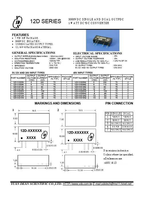
12D-XXD09N中文资料
- 格式:pdf
- 大小:69.10 KB
- 文档页数:1

用户手册020-000773-03H系列D12HD-H/D12WU-HThe CD included with this printed manual contains an electronic copy in English. Please read all instructions before using or servicing this product.Le DC fourni avec ce manuel imprimé contient une copie électronique en français. S'il vous plaît lire toutes les instructions avant d'utiliser ou de réparer ce produit.Die mit dieser gedruckten Anleitung gelieferte CD enthält eine elektronische Kopie in Deutsch. Bitte lesen Sie alle Anweisungen, bevor Sie dieses Produkt verwenden oder warten.Il CD fornito con il manuale stampato contiene una copia elettronica in lingua italiano. Si prega di leggere tutte le istruzioni prima di utilizzare o riparare questo prodotto.El DC incluido con este manual impreso contiene una copia electrónica en español. Por favor, lea todas las instrucciones antes de usar o dar servicio a este producto.注意事项版权和商标版权所有 © 2015 Christie Digital Systems USA, Inc. 保留所有权利。
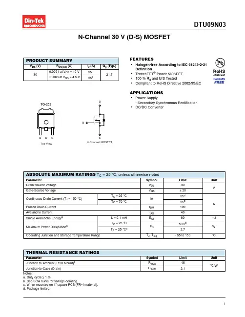
1N-Channel 30 V (D-S) MOSFETFEATURES•Halogen-free According to IEC 61249-2-21Definition•TrenchFET ® Power MOSFET •100 % R g and UIS Tested•Compliant to RoHS Directive 2002/95/ECAPPLICATIONS•Power Supply- Secondary Synchronous Rectification •DC/DC ConverterPRODUCT SUMMARYV DS (V)R DS(on) (Ω)I D (A)Q g (Typ.)300.0051 at V GS = 10 V 55d 21.70.0063 at V GS = 4.5 V55dNotes:a.Duty cycle ≤ 1 %.b.See SOA curve for voltage derating.c.When mounted on 1" square PCB (FR-4 material).d.Package limited.ABSOLUTE MAXIMUM RATINGS T C = 25 °C, unless otherwise notedParameterSymbol Limit Unit Drain-Source Voltage V DS 30VGate-Source VoltageV GS± 20Continuous Drain Current (T J = 150 °C)T C = 25 °C I D 55d AT C = 70 °C55d Pulsed Drain Current I DM 100Avalanche Current I AS40Single Avalanche Energy a L = 0.1 mHE AS 80mJ Maximum Power DissipationaT C = 25 °C P D 59.5b W T A = 25 °C c2.7Operating Junction and Storage T emperature RangeT J , T stg- 55 to 150°CTHERMAL RESISTANCE RATINGSParameterSymbol Limit Unit Junction-to-Ambient (PCB Mount)c R thJA 46°C/WJunction-to-Case (Drain)R thJC2.1TO-252S G D Top V ie w2Notes:a.Pulse test; pulse width ≤ 300 µs, duty cycle ≤ 2 %.b.Guaranteed by design, not subject to production testing.c.Independent of operating temperature.Stresses beyond those listed under “Absolute Maximum Ratings” may cause permanent damage to the device. These are stress ratings only, and functional operation of the device at these or any other conditions beyond those indicated in the operational sections of the specifications is not implied. Exposure to absolute maximum rating conditions for extended periods may affect device reliability.SPECIFICATIONS T J = 25 °C, unless otherwise notedParameter Symbol Test Conditions Min.Typ.Max.UnitStaticDrain-Source Breakdown Voltage V DS V DS = 0 V , I D = 250 µA 30V Gate Threshold Voltage V GS(th) V DS = V GS , I D = 250 µA 12.5Gate-Body LeakageI GSS V DS = 0 V, V GS = ± 20 V ± 250nAZero Gate Voltage Drain Current I DSS V DS = 30 V , V GS = 0 V 1µA V DS = 30 V , V GS = 0 V , T J = 125 °C 50V DS = 30 V , V GS = 0 V , T J = 150 °C250On-State Drain Current aI D(on)V DS ≥ 10 V , V GS = 10 V 55A Drain-Source On-State Resistance a R DS(on) V GS = 10 V, I D = 22 A 0.00420.0051ΩV GS = 4.5 V , I D = 20 A 0.00520.0063Forward T ransconductance a g fsV DS = 15 V , I D = 20 A110S Dynamic bInput Capacitance C iss V GS = 0 V , V DS = 15 V , f = 1 MHz2780pFOutput CapacitanceC oss 641Reverse Transfer Capacitance C rss 260Total Gate Charge c Q g V DS = 15 V , V GS = 10 V , ID = 20 A 4466nC V DS = 15 V , V GS = 4.5 V , I D = 20 A 21.732.6Gate-Source Charge c Q gs 7Gate-Drain Charge c Q gd 6.7Gate Resistance R g f = 1 MHz0.424ΩTurn-On Delay Time c t d(on) V DD = 15 V, R L = 1.5 ΩI D ≅ 10 A, V GEN = 10 V , R g = 1 Ω816ns Rise Time ct r 918Turn-Off Delay Time c t d(off) 3553Fall Time ct f 918Drain-Source Body Diode Ratings and Characteristics T C = 25°C bContinuous Current I S 55A Pulsed Current I SM 100Forward Voltage a V SD I F = 10 A, V GS = 0 V0.75 1.5V Reverse Recovery Time t rr I F = 10 A, dI/dt = 100 A/µs 3451ns Peak Reverse Recovery Current I RM(REC)23A Reverse Recovery ChargeQ rr3451nC3Transfer CharacteristicsTransconductance On-Resistance vs. Gate-to-Source Voltage4TYPICAL CHARACTERISTICS 25°C, unless otherwise notedCapacitanceOn-Resistance vs. Junction TemperatureDrain Source Breakdown vs. Junction TemperatureCurrent DeratingTYPICAL CHARACTERISTICS 25°C, unless otherwise notedSingle Pulse Avalanche Current Capability vs. TimeSafe Operating AreaNormalized Thermal Transient Impedance, Junction-to-Case51TO-252AA CASE OUTLINENote•Dimension L3 is for reference only.MILLIMETERSINCHESDIM.MIN.MAX.MIN.MAX.A 2.18 2.380.0860.094A1-0.127-0.005b 0.640.880.0250.035b20.76 1.140.0300.045b3 4.95 5.460.1950.215C 0.460.610.0180.024C20.460.890.0180.035D 5.97 6.220.2350.245D1 5.21-0.205-E 6.35 6.730.2500.265E1 4.32-0.170-H 9.4010.410.3700.410e 2.28 BSC 0.090 BSC e1 4.56 BSC 0.180 BSC L 1.40 1.780.0550.070L30.89 1.270.0350.050L4- 1.02-0.040L51.141.520.0450.060ECN: X12-0247-Rev. M, 24-Dec-12DWG: 53471A P P L I C A T I O N N O T ERECOMMENDED MINIMUM PADS FOR DPAK (TO-252)。

编号:XGN2-12高压开关柜使用说明书襄阳展宇电气有限公司XIANGFAN ZHANYU ELECTRIC CO.,LTD.公司地址:湖北省襄阳市春园西路101号技术服务:传真:(0710)3342898销售直拨:(0710)3343998 邮编:441000前言感谢您选用展宇电气XGN2-12型高压开关柜系列产品。
本说明书提供给用户安装、运行参数设定、异常诊断、日常维护及安全使用相关注意事项。
为了保证正确地安装及操作本产品,请在装机之前,详细阅读本使用说明书。
我们的服务就和我们的产品一样,全体员工一直坚信用户是上帝的原则。
如在使用过程中遇到解决不了的疑难问题,请联络本公司的各地经销商或直接与本公司联系。
产品购入后,请检查本产品是否因运输不慎而造成损伤;产品的规格、型号是否与订购产品的机种相符;有无合格标志等。
由于产品在不断地更新换代可能出现设备及产品的个别地方或文字与宣传资料不符,如果发现设备出现此种问题请咨询本公司。
拆箱后请检查设备前柜门内文件盒内的产品说明书。
如有问题,请与供货商联系。
希望用户妥善保管本说明书,这对今后的维护、保养以及其它应用的场合会有所俾益。
用户应将本说明书交给直接使用或操作人员手中,如需对本说明书存档,请与本公司联系,本公司将免费为您提供一套存档用说明书。
安全警告✧禁止野蛮搬运及安装,禁止雨淋,远离电磁干扰。
✧防止儿童和公众接触或接近本设备,本设备有危险电压。
✧本设备只能按照制造商规定的用途使用,未经授权的修改或不按本手册的规定操作可能会导致严重地人身伤害及其它伤害。
✧只有经过严格训练的专业操作人员及专业技术人员才能允许操作及维护本产品。
✧请在操作本设备前,认真阅读本手册中的所有安全说明安装操作和维护规程。
目录1、概述 (4)2、产品型号及含义 (4)3、主要技术数据 (4)4、结构概述 (6)5、使用说明 (7)6、安装 (7)7、维护要点 (8)8、包装、运输、存储和启封 (9)9、订货须知 (9)一、概述◆主要用途XGN2-12型高压开关柜,适用于3~10kV三相50HZ交流单母线系统,作为接受和分配电能用。

34 .80 7IRELESS IMPORTANT NOTICEDear customer,As from August 2nd2008, the wireless operations of NXP have moved to a new company,ST-NXP Wireless.As a result, the following changes are applicable to the attached document.●Company name - Philips Semiconductors is replaced with ST-NXP Wireless.●Copyright - the copyright notice at the bottom of each page “© Koninklijke PhilipsElectronics N.V. 200x. All rights reserved”, shall now read: “© ST-NXP Wireless 200x -All rights reserved”.●Web site - is replaced with●Contact information - the list of sales offices previously obtained by sending an emailto sales.addresses@, is now found at under Contacts.If you have any questions related to the document, please contact our nearest sales office.Thank you for your cooperation and understanding.ST-NXP Wireless34 .80 7IRELESS1.General descriptionThe PDIUSBD12is a cost-and feature-optimized USB peripheral controller.It is normallyused in microcontroller-based systems and communicates with the system microcontrollerover the high-speed general-purpose parallel interface. It also supports local DMAtransfer.This modular approach to implementing a USB interface allows the designer to choosethe optimum system microcontroller from the wide variety available. This flexibility cutsdown development time, risks and costs, by allowing the use of the existing architecture,minimizing firmware investments. This results in the fastest way to develop the mostcost-effective USB peripheral solution.The PDIUSBD12fully conforms to Universal Serial Bus Specification Rev.2.0,supportingdata transfer at full-speed (12Mbit/s).It is also designed to be compliant with most deviceclass specifications: imaging class, mass storage devices, communication devices,printing devices and human interface devices. The PDIUSBD12 is ideally suited for manyperipherals, such as printer, scanner, external mass storage (Zip drive) and digital stillcamera. It offers an immediate cost reduction for applications that currently use SCSIimplementations.The PDIUSBD12low suspend power consumption along with the LazyClock output allowsfor easy implementation of equipment that is compliant to the ACPI, OnNow and USBpower management requirements.The low operating power allows the implementation ofbus powered peripherals.It also incorporates features,such as SoftConnect,GoodLink,programmable clock output,low frequency crystal oscillator, and integration of termination resistors. All of thesefeatures contribute to significant cost savings in the system implementation and at the same time ease the implementation of advanced USB functionality into peripherals.2.Featuress Complies with Universal Serial Bus specification Rev.2.0s Supports data transfer at full-speed (12Mbit/s)s High performance USB peripheral controller with integrated SIE, FIFO memory,transceiver and voltage regulators Compliant with most device class specificationss High-speed (2MB/s) parallel interface to any external microcontroller ormicroprocessors Fully autonomous DMA operations Integrated 320B of multi-configuration FIFO memoryPDIUSBD12Universal Serial Bus peripheral controller with parallel busRev. 09 — 11 May 2006Product data sheets Double buffering scheme for main endpoint increases throughput and eases real-time data transfers Data transfer rates: 1MB/s achievable in bulk mode, 1Mbit/s achievable inisochronous modes Bus-powered capability with very good EMI performances Controllable LazyClock output during suspends Software-controllable connection to the USB bus (SoftConnect)s Good USB connection indicator that blinks with traffic (GoodLink)s Programmable clock frequency outputs Complies with the ACPI, OnNow and USB power management requirementss Internal Power-On Reset (POR) and low-voltage reset circuits Available in SO28 and TSSOP28 pin packagess Full industrial grade operation from−40°C to +85°Cs Full-scan design with high fault coverage (>99%) ensures high qualitys Operation with dual voltages: 3.3V±0.3V or extended 5V supply range of4.0V to5.5Vs Multiple interrupt modes to facilitate both bulk and isochronous transfers3.Ordering informationTable 1.Ordering informationOutside North America North America Package TemperaturerangeVersion Name DescriptionPDIUSBD12D PDIUSBD12D SO28plastic small outline package;28leads;body width 7.5mm−40°C to +85°C SOT136-1PDIUSBD12PW PDIUSBD12PW DH TSSOP28plastic thin shrink small outlinepackage; 28leads; body width 4.4mm−40°C to +85°C SOT361-14.Block diagram5.Pinning information5.1Pinning This is a conceptual block diagram and does not include each individual signal.Fig 1.Block diagram6 MHzD+D −PLL SoftConnect D+3.3 V1.5 k Ω004aaa796VOLTAGEREGULATOR ANALOGTX/RX PARALLELAND DMAINTERFACEMEMORY MANAGEMENTUNITINTEGRATED RAM PHILIPSSIE BIT CLOCK RECOVERY UPSTREAM PORT Fig 2.Pin configurationPDIUSBD12DATA0A0DATA1VOUT3.3DATA2D+DATA3D −GNDV CC DATA4XTAL2DATA5XTAL1DATA6GL_N DATA7RESET_NALE EOT_NCS_N DMACK_NSUSPEND DMREQCLKOUT WR_NINT_N RD_N004aaa532123456789101112131416151817201922212423262528275.2Pin descriptionTable 2.Pin descriptionSymbol Pin Type[1]DescriptionDA T A01IO2bit0 of bidirectional data; slew-rate controlledDA T A12IO2bit1 of bidirectional data; slew-rate controlledDA T A23IO2bit2 of bidirectional data; slew-rate controlledDA T A34IO2bit3 of bidirectional data; slew-rate controlledGND5P groundDA T A46IO2bit4 of bidirectional data; slew-rate controlledDA T A57IO2bit5 of bidirectional data; slew-rate controlledDA T A68IO2bit6 of bidirectional data; slew-rate controlledDA T A79IO2bit7 of bidirectional data; slew-rate controlledALE10I Address Latch Enable: The falling edge is used to close the latch ofthe address information in a multiplexed address or data bus.Permanently tied to LOW for separate address or data busconfiguration.CS_N11I chip select (active LOW)When the CS_N pin is LOW, ensure that the RESET_N pin is ininactive state; otherwise, the device will enter test mode.SUSPEND12I, OD4device is in the suspend stateCLKOUT13O2programmable output clock (slew-rate controlled)INT_N14OD4interrupt (active LOW)RD_N15I read strobe (active LOW)WR_N16I write strobe (active LOW).DMREQ17O4DMA requestDMACK_N18I DMA acknowledge (active LOW)EOT_N19I end of DMA transfer (active LOW); double up as V BUS sensing.EOT_N is only valid when asserted together with DMACK_N andeither RD_N or WR_N.RESET_N20I reset (active LOW and asynchronous); built-in power-on reset circuitis present on-chip, so the pin can be tied HIGH to V CCWhen the RESET_N pin is LOW, ensure that the CS_N pin is ininactive state; otherwise, the device will enter test mode.GL_N21OD8GoodLink LED indicator (active LOW)XT AL122I crystal connection1 (6MHz)XT AL223O crystal connection2 (6MHz); if the external clock signal, instead ofthe crystal, is connected to XTAL1, then XTAL2 should be floated V CC24P voltage supply (4.0V to5.5V)To operate the IC at3.3V,supply3.3V to both the V CC and VOUT3.3pins.D−25A USB D− data lineTable 2.Pin description …continuedSymbol Pin Type[1]DescriptionD+26A USB D+ data lineVOUT3.327P 3.3V regulated output; to operate the IC at 3.3V, supply a 3.3V toboth the V CC and VOUT3.3 pinsA028I address bitA0=1 —Selects the command instructionA0=0 —selects the data phaseThis bit is a don’t care in a multiplexed address and data busconfiguration and should be tied to HIGH.[1]P:power or ground;A:analog;I:input;O:Output;O2:Output with2mA drive;OD4:Output open-drain with4mA drive; OD8: Output open-drain with 8mA drive; IO2: Input and output with 2mA drive; O4: Output with 4mA drive.6.Functional description6.1Analog transceiverThe integrated transceiver directly interfaces to USB cables through termination resistors.6.2Voltage regulatorA 3.3V regulator is integrated on-chip to supply the analog transceiver. This voltage isalso provided as an output to connect to the external1.5kΩpull-up resistor.Alternatively,the PDIUSBD12 provides the SoftConnect technology with an integrated 1.5kΩ pull-upresistor.6.3PLLA 6MHz-to-48MHz clock multiplier Phase-Locked Loop (PLL) is integrated on-chip. Thisallows the use of a low-cost 6MHz crystal. ElectroMagnetic Interference (EMI) is alsominimized because of the lower frequency crystal. No external components are neededfor the operation of the PLL.6.4Bit clock recoveryThe bit clock recovery circuit recovers the clock from the incoming USB data stream using4×over-sampling principle. It can track jitter and frequency drift specified by UniversalSerial Bus Specification Rev.2.0.6.5Philips Serial Interface Engine (PSIE)The Philips SIE implements the full USB protocol layer. It is completely hardwired forspeed and needs no firmware intervention. The functions of this block include:synchronization pattern recognition,parallel or serial conversion,bit stuffing or discardingstuffed bits, CRC checking or generation, PID verification or generation, addressrecognition, and handshake evaluation or generation.6.6SoftConnectThe connection to the USB is accomplished by connecting D+(for full-speed USB device)to HIGH through a 1.5kΩ pull-up resistor. In the PDIUSBD12, the 1.5kΩ pull-up resistoris integrated on-chip and is not connected to V CC by default. The connection isestablished through a command sent by the external or system microcontroller. Thisallows the system microcontroller to complete its initialization sequence before deciding toestablish connection to the USB. Re-initialization of the USB bus connection can also beperformed without requiring to pull out the cable.The PDIUSBD12 will check for USB V BUS availability before the connection can beestablished.The V BUS sensing is provided using pin EOT_N.For details,see Section5.2.Sharing of the V BUS sensing and EOT_N can be easily accomplished by using the V BUSvoltage as the pull-up voltage for the normally open-drain output of the DMA controller pin.Remark:The tolerance of internal resistors is higher (25%) than that specified inUniversal Serial Bus Specification Rev.2.0(5%).The overall voltage specification for theconnection,however,can still be met with good margin.The decision to make sure of thisfeature lies with users.6.7GoodLinkA good USB connection indication is provided through the GoodLink technology. Duringenumeration, the LED indicator will momentarily blink on corresponding to theenumeration traffic. When the PDIUSBD12 is successfully enumerated and configured,the LED indicator will be permanently on.Subsequent successful (with acknowledgment)transfer to and from the PDIUSBD12 will blink off the LED. During suspend, the LED willbe off.This feature provides a user-friendly indication on the status of the USB device, theconnected hub and the USB traffic. It is a useful field diagnostics tool to isolate faultyequipment. This feature helps lower field support and hotline costs.6.8Memory Management Unit (MMU) and integrated RAMThe difference between MMU and the integrated RAM buffer lies in the speed betweenUSB, running in bursts of 12Mbit/s and the parallel interface to the microcontroller. Thisallows the microcontroller to read and write USB packets at its own speed.6.9Parallel and DMA interfaceA generic parallel interface is defined for ease-of-use and speed, and allows directinterfacing to major microcontrollers. To a microcontroller, the PDIUSBD12 appears as amemory device with 8-bit data bus and 1-bit address line (occupying two locations). ThePDIUSBD12 supports both multiplexed and non-multiplexed address and data bus. ThePDIUSBD12 also supports Direct Memory Access (DMA) transfer that allows the mainendpoint (endpoint 2) to directly transfer to and from the local shared memory. Bothsingle-cycle and burst mode DMA transfers are supported.6.10Example of parallel interface to an 80C51 microcontrollerIn the example shown in Figure 3, the ALE pin is permanently tied to LOW to signify aseparate address and data bus configuration. The A0 pin of the PDIUSBD12 connects toany of the 80C51 I/O ports. This port controls the command or data phase to thePDIUSBD12. The multiplexed address and data bus of the 80C51 can now be directlyconnected to the data bus of the PDIUSBD12. The address phase will be ignored by thePDIUSBD12. The clock input signal of the 80C51 (pin XTAL1) can be provided by outputCLKOUT of the PDIUSBD12.Fig 3.Example of a parallel interface to an 80C51 microcontrollerPDIUSBD1280C51INT_NA0DATA [7:0]WR_NRD_NCLKOUTCS_NALE XTAL1RD/P3.7WR/P3.6P [0.7:0.0]/AD [7:0]ANY I/O PORT (for example, P3.3)INTO/P3.2004aaa155ANY I/O PORT7.Direct Memory Access (DMA) transferDMA allows an efficient transfer of a block of data between the host and local sharedmemory. Using a DMA Controller (DMAC), the data transfer between the main endpoint(endpoint2) of the PDIUSBD12 and the local shared memory can occur autonomously,without the local CPU intervention.Preceding any DMA transfer, the local CPU receives from the host the necessary setupinformation and accordingly programs the DMA controller.Typically,the DMA controller isset up for demand transfer mode, and the Byte Count register and the address counterare programmed with the correct values. In this mode, transfers occur only when thePDIUSBD12 requests them and are terminated when the Byte Count register reacheszero.After the DMA controller is programmed,the DMA ENABLE bit of the PDIUSBD12isset by the local CPU to initiate the transfer.The PDIUSBD12 can be programmed for single-cycle DMA or burst mode DMA. Insingle-cycle DMA, the DMREQ pin is deactivated for every single acknowledgment byDMACK_N before being re-asserted. In burst mode DMA, the DMREQ pin is kept activefor the number of bursts programmed in the device before going inactive. This processcontinues until the PDIUSBD12 receives a DMA termination notice through pin EOT_N.This will generate an interrupt to notify the local CPU that the DMA operation iscompleted.For the DMA read operation,the DMREQ pin will only be activated whenever the buffer isfull,signaling that the host has successfully transferred a packet to the PDIUSBD12.Withthe double buffering scheme, the host can start filling up the second buffer while the firstbuffer is being read out.This parallel processing increases the effective throughput.Whenthe host does not completely fill up the buffer (less than 64B or 128B for single directionISO configuration), the DMREQ pin will be deactivated at the last byte of the buffer,regardless of the current DMA burst count.It will be re-asserted on the next packet with arefreshed DMA burst count.Similarly,for DMA write operations,the DMREQ pin remains active whenever the buffer isnot full.When the buffer isfilled up,the packet is sent over to the host on the next IN tokenand DMREQ will be reactivated if the transfer was successful. Also, the double bufferingscheme here will improve throughput. For non-isochronous transfer (bulk and interrupt),the buffer needs to be completelyfilled up by the DMA write operation before data is sentto the host. The only exception is at the end of DMA transfer, when the reception of theEOT_N pin will stop the DMA write operation and the buffer content will be sent to the hoston the next IN token.For isochronous transfers, the local CPU and DMA controller have to guarantee that theycan sink or source the maximum packet size in one USB frame (1ms).The assertion of pin DMACK_N automatically selects the main endpoint (endpoint2),regardless of the current selected endpoint. The DMA operation of the PDIUSBD12 canbe interleaved with normal I/O access to other endpoints.The DMA operation can be terminated by resetting the DMA ENABLE register bit or theassertion of EOT_N together with DMACK_N and either RD_N or WR_N.The PDIUSBD12 supports DMA transfer in single address mode and it can also work indual address mode of the DMA controller. In single address mode, the DMA transfer isdone using the DREQ, DMACK_N, EOT_N, WR_N and RD_N control lines. In dualaddress mode, pins DMREQ, DMACK_N and EOT_N are not used; instead CS_N,WR_N and RD_N control signals are used. The I/O mode transfer protocol of thePDIUSBD12 needs to be followed. The source of the DMAC is accessed during the readcycle and the destination during the write cycle.Transfer needs to be done in two separatebus cycles, temporarily storing data in the DMAC.8.Endpoint descriptionThe PDIUSBD12 endpoints are sufficiently generic to be used by various device classesranging from imaging, printer, mass storage and communication device classes. ThePDIUSBD12endpoints can be configured for four operating modes,depending on the SetMode command. The four modes are:Mode 0Non-isochronous transfer (Non-ISO mode)Mode 1Isochronous output only transfer (ISO-OUT mode)Mode 2Isochronous input only transfer (ISO-IN mode)Mode 3Isochronous input and output transfer (ISO-I/O mode)Table 3.Endpoint configurationEndpoint number Endpoint index Transfer type Direction[1]Max. Packet size (bytes) Mode0 (Non-ISO mode)00control OUT161IN1612generic[2]OUT163IN1624generic[2][3]OUT64[4]5IN64[4]Mode1 (ISO-OUT mode)00control OUT161IN1612generic[2]OUT163IN1624isochronous[3]OUT128[4]Mode2 (ISO-IN mode)00control OUT161IN1612generic[2]OUT163IN1625isochronous[3]IN128[4]Mode3 (ISO-I/O mode)00control OUT161IN1612generic[2]OUT163IN1624isochronous[3]OUT64[4]5IN64[4][1]IN: input for the USB host; OUT: output from the USB host.[2]Generic endpoints can be used either as bulk or interrupt endpoint.[3]The main endpoint (endpoint number2) is double-buffered to ease synchronization with real-timeapplications and to increase throughput. This endpoint supports DMA access.[4]Denotes double buffering. The size shown is for a single buffer.9.Main endpointThe main endpoint (endpoint number2) is the primary endpoint for sinking or sourcingrelatively large amounts of data. It implements the following features to ease this task:•Double buffering. This allows parallel operation between the USB access and thelocal CPU access, increasing throughput. Buffer switching is automatically handled.This results in transparent buffer operation.•DMA operation. This can be interleaved with normal I/O operation to other endpoints.•Automatic pointer handling during the DMA operation. No local CPU intervention isnecessary when ‘crossing’ the buffer boundary.•Configurable endpoint for either isochronous transfer or non-isochronous (bulk andinterrupt) transfer.mand summaryTable mand summaryName Destination Code (Hex)TransactionInitialization commandsSet Address/Enable device D0write 1BSet Endpoint Enable device D8write 1BSet Mode device F3write 2BSet DMA device FB write or read 1BData flow commandsRead Interrupt register device F4read 2BSelect Endpoint control OUT00read 1B (optional)control IN01read 1B (optional)endpoint1 OUT02read 1B (optional)endpoint1 IN03read 1B (optional)endpoint2 OUT04read 1B (optional)endpoint2 IN05read 1B (optional)Read Last T ransaction Status control OUT40read 1Bcontrol IN41read 1Bendpoint1 OUT42read 1Bendpoint1 IN43read 1Bendpoint2 OUT44read 1Bendpoint2 IN45read 1BRead Buffer selected endpoint F0read n BWrite Buffer selected endpoint F0write n Bmand description11.1Command procedureThere are three basic types of commands: initialization, data flow and general.Respectively, these are used to initialize the function; for data flow between the function and the host; and some general commands.11.2Initialization commandsInitialization commands are used during the enumeration process of the USB network.These commands are used to enable function endpoints. They are also used to set the USB assigned address.11.2.1Set Address/EnableCode (Hex) —D0Transaction —write 1BThis command is used to set the USB assigned address and enable the function.Set Endpoint Statuscontrol OUT 40write 1B control IN 41write 1B endpoint 1 OUT 42write 1B endpoint 1 IN 43write 1B endpoint 2 OUT 44write 1B endpoint 2 IN45write 1B Acknowledge Setup selected endpoint F1none Clear Buffer selected endpoint F2none Validate Buffer selected endpointFA none General commands Send ResumeF6none Read Current Frame NumberF5read 1 or 2BTable mand summary …continuedNameDestination Code (Hex)Transaction ADDRESS : The value written becomes the address.ENABLE : Logic 1 enables this function.Fig 4.Set Address/Enable command: bit allocation7654320100Power-on value ADDRESS ENABLE004aaa79700000011.2.2Set Endpoint EnableCode (Hex) —D8Transaction —write 1BThe generic or isochronous endpoints can only be enabled when the function is enabled using the Set Address/Enable command.11.2.3Set ModeCode (Hex) —F3Transaction —write 2BThe Set Mode command is followed by two data writes. The first byte contains configuration bits. The second byte is the clock division factor byte.GENERIC OR ISOCHRONOUS ENDPOINTS : Logic 1 indicates that generic or isochronous endpoints are enabled.Fig 5.Set Endpoint Enable command: bit allocation765432X 100Power-on valueGENERIC/ISOCHRONOUS ENDPOINTS reserved; write 0X X X X X X 004aaa798For bit allocation, see Table 5.Fig 6.Set Mode command, configuration byte: bit allocationPower-on value reserved NO LAZYCLOCK CLOCK RUNNING INTERRUPT MODE SoftConnect reserved; write 0ENDPOINT CONFIGURATION765432111001000004aaa799Table 5.Set Mode command, configuration byte: bit allocationBitSymbolDescription7 to 6ENDPOINTCONFIGURA TIONThese two bits set endpoint configurations as follows: Mode 0 (Non-ISO mode) Mode 1 (ISO-OUT mode) Mode 2 (ISO-IN mode) Mode 3 (ISO-I/O mode) For details, see Section 8.4SoftConnectLogic 1indicates that the upstream pull-up resistor will be connected if V BUS is available. Logic 0 means that the upstream resistor will not be connected. The programmed value will not be changed by a bus reset.3INTERRUPT MODELogic 1 indicates that all errors and ‘NAK’ are reported and willgenerate an interrupt.Logic 0indicates that only OK is reported.The programmed value will not be changed by a bus reset.2CLOCK RUNNINGLogic 1 indicates that internal clocks and PLL are always running even during the suspend state. Logic 0 indicates that the internal clock, crystal oscillator and PLL are stopped, whenever not needed.To meet the strict suspend current requirement,this bit must be set to logic 0. The programmed value will not be changed by a bus reset.1NO LAZYCLOCKLogic 1 indicates that CLKOUT will not switch to LazyClock. Logic 0indicates that CLKOUT switches to LazyClock 1ms after theSUSPEND pin goes HIGH. LazyClock frequency is 30kHz ±40%.The programmed value will not be changed by a bus reset.For bit allocation, see Table 6.Fig 7.Set Mode command, clock division factor byte: bit allocation7654321110Power-on value10X X 00CLOCK DIVISION FACTOR reserved 004aaa800SET_TO_ONESOF-ONLY INTERRUPT MODE11.2.4Set DMACode (Hex) —FBTransaction —read or write 1BThe Set DMA command is followed by one data write or read to or from the DMA Configuration register.11.2.4.1DMA Configuration registerDuring the DMA operation, the 2B buffer header (status and byte length information) is not transferred to or from the local CPU. This allows the DMA data to be continuous and not interleaved by chunks of these headers. For DMA read operations, the header will be skipped by the PDIUSBD12.See Section 11.3.5command.For DMA write operations,the header will be automatically added by the PDIUSBD12.This provides a clean and simple DMA data transfer.Table 6.Set Mode command, clock division factor byte: bit allocationBit SymbolDescription7SOF-ONL YINTERRUPT MODE Setting this bit to logic 1will cause the interrupt line to be activated because of the Start-Of-Frame (SOF) clock only, regardless of the setting of PIN-INTERRUPT MODE, bit 5 of Set DMA.6SET_TO_ONEThis bit must be set to logic 1 before any DMA read or DMA write operation. This bit should always be set to logic 1 after power. It is zero after power-on reset.3to 0CLOCK DIVISIONFACTORThe value indicates the clock division factor for CLKOUT . Theoutput frequency is 48MHz /(N +1), where N is the clock division factor. The reset value is 11. This will produce an output frequency of 4MHz that can then be programmed up or down by the user.The minimum value is 1, giving a frequency range of4MHz to 24MHz.The minimum value of N is 0,giving a maximum frequency of 48MHz. The maximum value of N is 11, giving aminimum frequency of 4MHz.The PDIUSBD12design ensures no glitching during frequency change. The programmed value will not be changed by a bus reset.For bit allocation, see Table 7.Fig 8.Set DMA command: bit allocationPower-on value INTERRUPT PIN MODEENDPOINT INDEX 4 INTERRUPT ENABLE ENDPOINT INDEX 5 INTERRUPT ENABLE7654320100000000DMA ENABLE DMA DIRECTION AUTO RELOAD DMA BURST 004aaa80111.3Data flow commandsData flow commands are used to manage the data transmission between USB endpoints and the external microcontroller.Much of the data flow is initiated using an interrupt to the microcontroller. The microcontroller utilizes these commands to access and determine whether endpoint FIFOs have valid data.11.3.1Read Interrupt registerCode (Hex) —F4Transaction —read 2BTable 7.Set DMA command: bit allocation Bit SymbolDescription7ENDPOINT INDEX 5INTERRUPT ENABLELogic 1 allows an interrupt to be generated whenever the endpoint buffer is validated (see Section 11.3.8 command).Normally turned off for the DMA operation to reduce unnecessary CPU servicing.6ENDPOINT INDEX 4INTERRUPT ENABLELogic 1 allows an interrupt to be generated whenever the endpoint buffer contains a valid packet. Normally turned off for the DMA operation to reduce unnecessary CPU servicing.5INTERRUPT PIN MODELogic 0 signifies a normal interrupt pin mode in which an interrupt is generated as a logical OR of all the bits in interrupt registers. Logic 1 signifies that the interrupt will occur when SOF clock is seen on the upstream USB bus.The other normal interrupts are still active.4AUTO RELOAD When this bit is set to logic 1, the DMA operation will automatically restart.3DMA DIRECTIONThis bit determines the direction of data flow during a DMA transfer.Logic 1means from the external shared memory to the PDIUSBD12 (DMA write); logic 0 means from the PDIUSBD12 to the external shared memory (DMA read).2DMA ENABLEWriting logic 1to this bit will start the DMA operation through the assertion of pin DMREQ.The main endpoint buffer must be full (for DMA read) or empty (for DMA write), before DMREQ is asserted. In single cycle DMA mode, the DMREQ is deactivated on receiving DMACK_N. In burst mode DMA, the DMREQ is deactivated after the number of burst is exhausted. It is then asserted again for the next burst. This process continues until EOT_N is assertedtogether with DMACK_N and either RD_N or WR_N, which will reset this bit to logic 0and terminate the DMA operation.The DMA operation can also be terminated by writing logic 0to this bit.1to 0DMA BURSTSelects the burst length for DMA operation: 00Single-cycle DMA 01Burst (4-cycle) DMA 10Burst (8-cycle) DMA 11Burst (16-cycle) DMA。