NCP1593AMNTWG,NCP1593BMNTWG, 规格书,Datasheet 资料
- 格式:pdf
- 大小:403.22 KB
- 文档页数:13
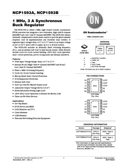
NCP1593A, NCP1593B1 MHz, 3 A Synchronous Buck RegulatorThe NCP1593 is a fixed 1 MHz, high−output−current, synchronous PWM converter that integrates a low−resistance, high−side P−channel MOSFET and a low−side N−channel MOSFET. The NCP1593 utilizes internally compensated current mode control to provide good transient response, ease of implementation and excellent loop stability. It regulates input voltages from 4.0 V to 5.5 V down to an output voltage as low as 0.6 V and is able to supply up to 3 A of load current.The NCP1593 includes an internally fixed switching frequency (F SW), and an internal soft−start to limit inrush current. Other features include cycle−by−cycle current limiting, 100% duty cycle operation, short− circuit protection, power saving mode and thermal shutdown. Features•Wide Input V oltage Range: from 4.0 V to 5.5 V•Internal 90 m W High−Side P−Channel MOSFET and 60 m W Low−Side N−Channel MOSFET•Fixed 1 MHz Switching Frequency•Cycle−by−Cycle Current Limiting•Hiccup Mode Short−Circuit Protection•Overtemperature Protection•Internal Soft−Start•Start−up with Pre−Biased Output Load •Adjustable Output V oltage Down to 0.6 V •Diode Emulation During Light Load•100% Duty Cycle Operation to Extend the Battery Life •These are Pb−Free DevicesApplications•Set−T op Boxes•DVD Drives and HDD•LCD Monitors and TVs•Cable Modems•USB Modems•Telecom/Networking/Datacom EquipmentDevice Package Shipping†ORDERING INFORMATIONNCP1593AMNTWG DFN10(Pb−Free)3000 / Tape &ReelDFN10CASE 485CMARKINGDIAGRAMS†For information on tape and reel specifications, including part orientation and tape sizes, please refer to our T ape and Reel Packaging Specifications Brochure, BRD8011/D.VCCPVCCPVCCANCLXLX(Top View)PIN CONNECTIONSA= Assembly LocationL= Wafer LotY= YearW= Work WeekG= Pb−Free Package1593AALYW GG(Note: Microdot may be in either location)SSPGFBENNCP1593BMNTWGVCCPVCCPVCCALXLXLX(Top View)NCPGFBEN1593BALYW GGDFN10(Pb−Free)3000 / Tape &ReelBLOCK DIAGRAMFigure 1. Block DiagramVCCPLXPGNDVCCENFBPGLXSS PIN DESCRIPTIONSPin No Symbol Description1NC / LX No connect pin for NCP1593A. The user may ground this pin or leave it floating. / LX pin for NCP1593B 2, 3LX The drains of the internal MOSFETs. The output inductor should be connected to these pins.4PG Open drain output from the Power Good logic. When the FB voltage is within regulation, this is a high impedance pin. Otherwise it is pulled low.5EN Logic input to enable the part. Logic high to turn on the part and a logic low to shut off the part. An intern-al pullup forces the part into an enable state when no external bias is present on the pin.6FB Feedback input pin of the Error Amplifier. Connect a resistor divider from the converter’s output voltage to this pin to set the converter’s regulated voltage.7SS / NC An external capacitor on this pin sets the soft −start ramp time. Leaving this pin open sets the soft −start time at 500 m s. For NCP1593B this pin is a no connect and should be left floating.8V CC Input supply pin for internal bias circuitry. Connect a 0.1 m F ceramic bypass capacitor to this pin. Directly connect the V CC pin to the V CCP pin on the board.9, 10V CCP Input for the power stageEPGNDExposed pad of the package provides both electrical contact to the ground and good thermal contact to the PCB. This pad must be soldered to the PCB for proper operation.APPLICATION CIRCUITFigure 2. Recommended Application CircuitV inV outABSOLUTE MAXIMUM RATINGSRatingSymbol Value Unit Power Supply Pin (Pins 8, 9, 10) to GNDV in6.5−0.3 (DC)−1.0 (t < 100 ns)VLX to GND V in + 0.7V in + 1.0 (t < 20 ns)−0.7 (DC)−5.0 (t < 100 ns)VAll other pins 6.0−0.3 (DC)−1.0 (t < 100 ns)VOperating Ambient Temperature Range (Note 1)T A −40 to +85°C Operating Junction Temperature Range (Note 1)T J −40 to +125°C Maximum Junction Temperature T J(MAX)+150°C Storage Temperature RangeT S −55 to +150°C Thermal Resistance Junction −to −Air (Note 2)R q JA68°C/WStresses exceeding Maximum Ratings may damage the device. Maximum Ratings are stress ratings only. Functional operation above the Recommended Operating Conditions is not implied. Extended exposure to stresses above the Recommended Operating Conditions may affect device reliability.1.The maximum package power dissipation limit must not be exceeded.P D +T J(max)*T AR q JA2.R q JA measured on approximately 1x1 inch sq. of 1 oz. Copper FR −4 or G −10 board.ELECTRICAL CHARACTERISTICS (−40°C < T J < 125°C, V CC = 4.0 V − 5.5 V, for min/max values unless noted otherwise) Parameter Symbol Test Conditions Min Typ Max Unit Input Voltage Range V IN 4.0 5.5V V CC UVLO Threshold V UVLO 2.4 2.5 2.9V UVLO Hysteresis V UVLO_hys320mV V CC Quiescent Current I INVCC 1.0 1.5mA VCCP Quiescent Current I INVCCP2050m A Shutdown Supply Current I QSHDN 1.8 3.0m A FEEDBACK VOLTAGEReference Voltage V FB0.5910.60.609V Reference Voltage V FB T J = 25°C0.5940.60.606V Feedback Input Bias Current I FB10100nA Feedback Voltage Line Regulation (Note 3)V CC = 4.0 V to 5.5 V−65dB PWMMaximum Duty Cycle (Regulating) d.c.MAX95% Maximum Duty Cycle (LDO mode) d.c.LDO Vout > d.c.MAX* V IN100% Minimum Controllable On Time t ONmin35ns Current LimitCycle-by-cycle Current Limit (Note 3)I LIM V CC = 5.0 V, T J = 25°C 5.1A OscillatorSwitching Frequency f SW0.87 1.0 1.13MHz MOSFET’sHigh-Side MOSFET On Resistance R DSonH I DS = 100 mA, V IN = 5.0 V90190m W High-Side MOSFET Leakage I lkgH LX = 0 V10m A Low-Side MOSFET On Resistance R DSonL I DS = 100 mA, V IN = 5.0 V6090m W Low-Side MOSFET Leakage I lkgL LX = 5 V10m A POWER GOODPower Good Rising Threshold V PGH0.510.54V Power Good Falling Threshold V PHL0.480.51V Power Good Hysteresis (High-to-Low)V PGhys30mV Power Good Pulldown Voltage V RPG I PG = 2.5 mA130250mV ENABLEEnable High Threshold V ENHI 1.4V Enable Low Threshold V ENLO0.4V Enable Hysteresis V ENhys200mV Enable Pullup Current I EN 1.4 3.0m A Soft-StartDefault Soft-start Ramp Time t SS SS = open; f SW = 1MHz0.50.580.65ms Maximum Soft-start Ramp time t SS SS = max cap; f SW = 1MHz10ms Hiccup Timer 4 * t SS ms Soft-start Current I SS0.510.70.87m A Thermal ShutdownThermal Shutdown Threshold185°C Thermal Shutdown Hysteresis30°C 3.Guaranteed by Characterization.Figure 3. Efficiency vs. Output Current (3.3 V)Figure 4. Efficiency vs. Output Current (1.8 V)I OUT , OUTPUT CURRENT (A)I OUT , OUTPUT CURRENT (A)Figure 5. Efficiency vs. Output Current (1.05 V)Figure 6. Load Regulation (3.3 V)I OUT , OUTPUT CURRENT (A)I OUT , OUTPUT CURRENT (A)Figure 7. Load Regulation (1.8 V)Figure 8. Load Regulation (1.05 V)I OUT , OUTPUT CURRENT (A)I OUT , OUTPUT CURRENT (A)E F F I C I E N C Y (%)E F F I C I E N C Y (%)E F F I C I E N C Y (%)V O U T , O U T P U T V O L T A G E (V )V O U T , O U T P U T V O L T A G E (V )V O U T , O U T P U T V O L T A G E (V )Figure 9. Current Limit vs. TemperatureFigure 10. Current Limit vs. Input VoltageT J , JUNCTION TEMPERATURE (°C)INPUT VOLTAGE (V)5.505.255.004.754.504.254.003.503.754.004.254.755.005.255.50Figure 11. R DS(ON) vs. TemperatureFigure 12. Load Transient ResponseT J , JUNCTION TEMPERATURE (°C)Figure 13. Load Transient Response Figure 14. No Load Switching (1.05 V)P E A K C U R R E N T L I M I T (A )P E A K C U R R E N T L I M I T (A )R D S (O N ) (m W )4.50(VIN = 5 V, VOUT = 1.05 V, IOUT = 0.5 A to 3.0 A)Upper Trace: Output Voltage, 50 mV / div Lower Trace: Output Current, 2 A / divTime = 200 m s/div(VIN = 5 V, VOUT = 1.05 V, IOUT = 0.5 A to 3.0 A)Upper Trace: Output Voltage, 50 mV / div Lower Trace: Output Current, 2 A / divTime = 200 m s/div(VIN = 5 V, VOUT = 1.05 V, IOUT = 0 A)Upper Trace: LX Pin Switching Waveforms, 5 V / divMiddle Trace: Output Voltage, 20 mV / div Lower Trace: Inductor Current, 100 mA / divTime = 20 m s / divFigure 15. No Load Switching (1.8 V)Figure 16. No Load Switching (3.3 V)Figure 17. DCM Switching (1.05 V)Figure 18. DCM Switching (1.8 V)Figure 19. DCM Switching (3.3 V)Figure 20. CCM Switching (1.8 V)(VIN = 5 V, VOUT = 1.8 V, IOUT = 0 A)Upper Trace: LX Pin Switching Waveforms, 5 V / divMiddle Trace: Output Voltage, 20 mV / div Lower Trace: Inductor Current, 100 mA / divTime = 10 m s / div (VIN = 5 V, VOUT = 3.3 V, IOUT = 0 A)Upper Trace: LX Pin Switching Waveforms, 5 V / divMiddle Trace: Output Voltage, 20 mV / div Lower Trace: Inductor Current, 200 mA / divTime = 10 m s / div(VIN = 5 V, VOUT = 1.05 V, IOUT = 100 mA)Upper Trace: LX Pin Switching Waveforms, 5 V / divMiddle Trace: Output Voltage, 20 mV / div Lower Trace: Inductor Current, 200 mA / divTime = 500 ns / div (VIN = 5 V, VOUT = 1.8 V, IOUT = 150 A)Upper Trace: LX Pin Switching Waveforms, 5 V / divMiddle Trace: Output Voltage, 20 mV / div Lower Trace: Inductor Current, 200 mA / divTime = 500 ns / div(VIN = 5 V, VOUT = 3.3 V, IOUT = 100 mA)Upper Trace: LX Pin Switching Waveforms, 5 V / divMiddle Trace: Output Voltage, 20 mV / div Lower Trace: Inductor Current, 200 mA / divTime = 500 ns / div (VIN = 5 V, VOUT = 1.8 V, IOUT = 3 A)Upper Trace: LX Pin Switching Waveforms, 5 V / divMiddle Trace: Output Voltage, 20 mV / div Lower Trace: Inductor Current, 2 A / divTime = 500 ns / divFigure 21. Power On from Input VoltageFigure 22. Power Off from Input VoltageFigure 23. Power On from Enable Figure 24. Power On from Enable CSS = 4.7 nFigure 25. Power Off from Enable Figure 26. Short Circuit Operation(VIN = 5 V, VOUT = 1.8 V, IOUT = 3 A)Upper Trace: Input Voltage, 5 V / divSecond Trace: Power Good Pin Voltage, 5 V / divThird Trace: Output Voltage, 2 V / div Lower Trace: Inductor Current, 2 A / divTime = 1 ms / div(VIN = 5 V, VOUT = 1.8 V, IOUT = 3 A)Upper Trace: Input Voltage, 5 V / divSecond Trace: Power Good Pin Voltage, 5 V / divThird Trace: Output Voltage, 2 V / div Lower Trace: Inductor Current, 2 A / divTime = 200 m s / div(VIN = 5 V, VOUT = 1.8 V, IOUT = 3 A, no CSS)Upper Trace: Enable Pin Voltage, 5 V / div Second Trace: Power Good Pin Voltage, 5 V / divThird Trace: Output Voltage, 2 V / div Lower Trace: Inductor Current, 2 A / divTime = 2 ms / div (VIN = 5 V, VOUT = 1.8 V, IOUT = 3 A, CSS = 4.7 nF)Upper Trace: Enable Pin Voltage, 5 V / div Second Trace: Power Good Pin Voltage, 5 V / divThird Trace: Output Voltage, 2 V / div Lower Trace: Inductor Current, 2 A / divTime = 2 ms / div(VIN = 5 V, VOUT = 1.8 V, IOUT = 3 A)Upper Trace: Enable Pin Voltage, 5 V / div Second Trace: Power Good Pin Voltage, 5 V / divThird Trace: Output Voltage, 2 V / div Lower Trace: Inductor Current, 2 A / divTime = 200 m s / div(VIN = 5 V, VOUT = 1.8 V, IOUT = Current Limit, no CSS)Upper Trace: LX Pin Voltage, 5 V / div Middle Trace: Output Voltage, 2 V / div Lower Trace: Inductor Current, 2 A / divTime = 500 m s / divDETAILED DESCRIPTION OverviewThe NCP1593 is a synchronous PWM controller that incorporates all the control and protection circuitry necessary to satisfy a wide range of applications. The NCP1593 employs current mode control to provide fast transient response, simple compensation, and excellent stability. The features of the NCP1593 include a precision reference, fixed 1 MHz switching frequency, a transconductance error amplifier, an integrated high−side P−channel MOSFET and low−side N−Channel MOSFET, internal soft−start, and very low shutdown current. The protection features of the NCP1593 include internal soft−start, pulse−by−pulse current limit, and thermal shutdown.Reference VoltageThe NCP1593 incorporates an internal reference that allows output voltages as low as 0.6 V. The tolerance of the internal reference is guaranteed over the entire operating temperature range of the controller. The reference voltage is trimmed using a test configuration that accounts for error amplifier offset and bias currents.Oscillator FrequencyA fixed precision oscillator is provided. The oscillator frequency range is 1 MHz with $13% variation. Transconductance Error AmplifierThe transconductance error amplifier’s primary function is to regulate the converter’s output voltage using a resistor divider connected from the converter’s output to the FB pin of the controller, as shown in the applications schematic. If a Fault occurs, the amplifier’s output is immediately pulled to GND and PWM switching is inhibited.Soft−StartTo limit the startup inrush current, a soft−start circuit is used to ramp up the reference voltage from 0 V to its final value linearly. This soft−start time is internally set to a typical value of 500 m s, or it can be externally adjusted by adding a capacitor (C SS) from the SS pin to GND. The following formulas show how to set the externally adjustable soft-start time. The maximum allowable C SS is 10 nF.t SS+ǒCSSV FBǓI SS(eq. 1) Where:V FB: Reference voltage, typically 0.6 VI SS: Soft−start current, typically 0.7 m AOutput MOSFETsThe NCP1593 includes low R DS(on), both high−side P−channel and low−side N−channel MOSFETs capable of delivering up to 3.0 A of current. When the controller is disabled or during a Fault condition, the controller’s output stage is tri−stated by turning OFF both the upper and lower MOSFETs.Pulse Width ModulationA high−speed PWM comparator, capable of pulse widths as low as 35 ns, is included in the NCP1593. The inverting input of the comparator is connected to the output of the error amplifier. The non−inverting input is connected to the the current sense signal. At the beginning of each PWM cycle, the CLK signal sets the PWM flip−flop and the upper MOSFET is turned ON. When the current sense signal rises above the error amplifier’s voltage then the comparator will reset the PWM flip−flop and the upper MOSFET will be turned OFF.Current SenseThe NCP1593 monitors the current in the upper MOSFET. The current signal is required by the PWM comparator and the pulse−by−pulse current limiter.PROTECTIONSUndervoltage Lockout (UVLO)The under voltage lockout feature prevents the controller from switching when the input voltage is too low to power the internal power supplies and reference. Hysteresis is incorporated in the UVLO comparator to prevent resistive drops in the wiring or PCB traces from causing ON/OFF cycling of the controller during heavy loading at power up or power down.Overcurrent Protection (OCP)NCP1593 detects high side switch current and then compares to a voltage level representing the overcurrent threshold limit. If the current through the high side FET exceeds the overcurrent threshold limit for seven consecutive switching cycles, overcurrent protection is triggered.Once the overcurrent protection occurs, hiccup mode engages. First, hiccup mode, turns off both FETs and discharges the internal compensation network at the output of the OTA. Next, the IC waits typically 4 x t SS ms and then resets the overcurrent counter. After this reset, the circuit attempts another normal soft−start. Hiccup mode reduces input supply current and power dissipation during a short circuit. It also allows for much improved system up−time, allowing auto−restart upon removal of a temporary short−circuit.Pre−Bias StartupIn some applications the controller will be required to start switching when it’s output capacitors are charged anywhere from slightly above 0 V to just below the regulation voltage. This situation occurs for a number of reasons: the converter’s output capacitors may have residual charge on them or the converter’s output may be held up by a low current standby power supply. NCP1593 supports pre−bias start up by holding off switching off until the soft start ramp reaches the FB Pin voltage.Power GoodPower Good (PG) is an open-drain output that requires a pull−up resistor. It is actively held low in soft−start, standby, and shutdown. PG releases when the FB voltage and thus the output voltage rises above 90% of nominal regulation point. The PG goes low when the FB voltage falls below 85% of the regulation point.Thermal ShutdownThe NCP1593 protects itself from over heating with an internal thermal monitoring circuit. If the junction temperature exceeds the thermal shutdown threshold both the upper and lower MOSFETs will be shut OFF.APPLICATION INFORMATION Programming the Output VoltageThe output voltage is set using a resistive voltage dividerfrom the output voltage to FB pin (see Figure 27). So theoutput voltage is calculated according to Eq.1.V out+V FB@R1)R2R2(eq. 2)Figure 27. Output dividerInductor SelectionThe inductor is the key component in the switching regulator. The selection of inductor involves trade−offs among size, cost and efficiency. The inductor value is selected according to the equation 2.L+V outf@I ripple@ǒ1*V out V in(max)Ǔ(eq. 3)Where V out− the output voltage;f− switching frequency, 1.0 MHz;I ripple− Ripple current, usually it’s 20% − 30% of output current;V in(max)− maximum input voltage.Choose a standard value close to the calculated value to maintain a maximum ripple current within 30% of the maximum load current. If the ripple current exceeds this 30% limit, the next larger value should be selected.The inductor’s RMS current rating must be greater than the maximum load current and its saturation current should be about 30% higher. For robust operation in fault conditions (start−up or short circuit), the saturation current should be high enough. To keep the efficiency high, the series resistance (DCR) should be less than 0.1 W, and the core material should be intended for high frequency applications. Output Capacitor SelectionThe output capacitor acts to smooth the dc output voltage and also provides energy storage. So the major parameter necessary to define the output capacitor is the maximum allowed output voltage ripple of the converter. This ripple is related to capacitance and the ESR. The minimum capacitance required for a certain output ripple can be calculated by Equation 4.C OUT(min)+I ripple8@f@V ripple(eq. 4)Where V ripple is the allowed output voltage ripple.The required ESR for this amount of ripple can be calculated by equation 5.ESR+V rippleI ripple(eq. 5) Based on Equation 3 to choose capacitor and check its ESR according to Equation 4. If ESR exceeds the value from Eq.4, multiple capacitors should be used in parallel. Ceramic capacitor can be used in most of the applications. In addition, both surface mount tantalum and through−hole aluminum electrolytic capacitors can be used as well. Input Capacitor SelectionThe input capacitor can be calculated by Equation 6.C in(min)+I out(max)@D max@1f@V in(ripple)(eq. 6) Where V in(ripple) is the required input ripple voltage.D max+V outV in(min)is the maximum duty cycle.(eq. 7)Power DissipationThe NCP1593 is available in a thermally enhanced 10−pin, DFN package. When the die temperature reaches +185°C, the NCP1593 shuts down (see the Thermal−Overload Protection section). The power dissipated in the device is the sum of the power dissipated from supply current (PQ), power dissipated due to switching the internal power MOSFET (P SW), and the power dissipated due to the RMS current through the internal power MOSFET (PON). The total power dissipated in the package must be limited so the junction temperature does not exceed its absolute maximum rating of +150°C at maximum ambient temperature. Calculate the power lost in the NCP1593 using the following equations:1.High side MOSFETThe conduction loss in the top switch is:P HSON+I2RMS_HSFET R DS(on)HS(eq. 8) Where:I RMS_FET+ǒI out2)D I PP212ǓDǸ(eq. 9)D I PP is the peak−to−peak inductor current ripple.The power lost due to switching the internal power high side MOSFET is:P HSSW +V in @I out @ǒt r )t f Ǔ@f SW2(eq. 10)t r and t f are the rise and fall times of the internal power MOSFET measured at SW node. Typical rise times are 4 ns (rising) and 2 ns (falling).2.Low side MOSFETThe power dissipated in the top switch is:P LSON +I RMS_LSFET 2@R DS(on)LS(eq. 11)Where:I RMS_LSFET +ǒI out2)D I PP 212Ǔ@(1*D )Ǹ(eq. 12)D I PP is the peak −to −peak inductor current ripple.The switching loss for the low side MOSFET can be ignored.The power lost due to the quiescent current (I Q ) of the device is:P Q +V in @I Q(eq. 13)I Q is the switching quiescent current of the NCP1593.P TOTAL +P HSON )P HSSW )P LSON )P Q(eq. 14)Calculate the temperature rise of the die using the following equation:T J +T C )ǒP TOTAL @q JA Ǔ(eq. 15)q JC is the junction −to −case thermal resistance equal to 68°C/W. T A is the ambient temperature and TJ is the junction temperature, or die temperature. Solder the underside −exposed pad to a large copper GND plane. If thedie temperature reaches the thermal shutdown threshold the NCP1593 shut down and does not restart again until the die temperature cools by 30°C.Layout ConsiderationAs with all high frequency switchers, when considering layout, care must be taken in order to achieve optimal electrical, thermal and noise performance. For 1.0MHz switching frequency, switch rise and fall times are typically in few nanosecond range. To prevent noise both radiated and conducted the high speed switching current path must be kept as short as possible. Shortening the current path will also reduce the parasitic trace inductance of approximately 25 nH/inch. At switch off, this parasitic inductance produces a flyback spike across the NCP1593 switch. When operating at higher currents and input voltages, with poor layout, this spike can generate voltages across the NCP1593that may exceed its absolute maximum rating. A ground plane should always be used under the switcher circuitry to prevent interplane coupling and overall noise.The FB component should be kept as far away as possible from the switch node. The ground for these components should be separated from the switch current path. Failure to do so will result in poor stability or subharmonic like oscillation.Board layout also has a significant effect on thermal resistance. Reducing the thermal resistance from ground pin and exposed pad onto the board will reduce die temperature and increase the power capability of the NCP1593. This is achieved by providing as much copper area as possible around the exposed pad. Adding multiple thermal vias under and around this pad to an internal ground plane will also help. Similar treatment to the inductor pads will reduce any additional heating effects.PACKAGE DIMENSIONSDFN10 3x3, 0.5PCASE 485CISSUE B ArrayDIMENSIONS: MILLIMETERS*For additional information on our Pb−Free strategy and solderingdetails, please download the ON Semiconductor Soldering andMounting Techniques Reference Manual, SOLDERRM/D.ON Semiconductor and are registered trademarks of Semiconductor Components Industries, LLC (SCILLC). SCILLC owns the rights to a number of patents, trademarks, copyrights, trade secrets, and other intellectual property. A listing of SCILLC’s product/patent coverage may be accessed at /site/pdf/Patent−Marking.pdf. SCILLC reserves the right to make changes without further notice to any products herein. SCILLC makes no warranty, representation or guarantee regarding the suitability of its products for any particular purpose, nor does SCILLC assume any liability arising out of the application or use of any product or circuit, and specifically disclaims any and all liability, including without limitation special, consequential or incidental damages. “Typical” parameters which may be provided in SCILLC data sheets and/or specifications can and do vary in different applications and actual performance may vary over time. All operating parameters, including “Typicals” must be validated for each customer application by customer’s technical experts. SCILLC does not convey any license under its patent rights nor the rights of others. SCILLC products are not designed, intended, or authorized for use as components in systems intended for surgical implant into the body, or other applications intended to support or sustain life, or for any other application in which the failure of the SCILLC product could create a situation where personal injury or death may occur. Should Buyer purchase or use SCILLC products for any such unintended or unauthorized application, Buyer shall indemnify and hold SCILLC and its officers, employees, subsidiaries, affiliates, and distributors harmless against all claims, costs, damages, and expenses, and reasonable attorney fees arising out of, directly or indirectly, any claim of personal injury or death associated with such unintended or unauthorized use, even if such claim alleges that SCILLC was negligent regarding the design or manufacture of the part. SCILLC is an Equal Opportunity/Affirmative Action Employer. This literature is subject to all applicable copyright laws and is not for resale in any manner.PUBLICATION ORDERING INFORMATION。