第六章 光电探测器分解
- 格式:ppt
- 大小:1.62 MB
- 文档页数:69
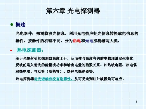
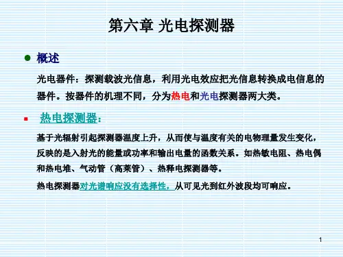
光电探测器光电探测器是利用辐射引起被照射材料电导率改变的一种物理现象的原理而制成的器件。
它的的工作原理是基于光电效应(包括外电光效应和内电光效应)。
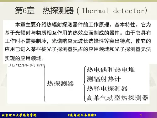
根据器件对辐射响应的方式不同或者说器件工作的机理不同,光电探测器可分为两大类:一类是光子型探测器;另一类是热探测器。
其中光子探测器包括真空光电器件(光电倍增管等)和固体光电探测器(光电二极管、光导探测器、CCD等)。
1光子探测器1)原理光子探测器利用外光电效应制成的光子型探测器是真空电子器件,如光电管、光电倍增管和红外变像管等。
这些器件都包含一个对光子敏感的光电阴极,当光子投射到光电阴极上时,光子可能被光电阴极中的电子吸收,获得足够大能量的电子能逸出光电阴极而成为自由的光电子。
在光电管中,光电子在带正电的阳极的作用下运动,构成光电流。
光电倍增管与光电管的差别在于,在光电倍增管的光电阴极与阳极之间设置了多个电位逐级上升并能产生二次电子的电极(称为打拿极)。
从光电阴极逸出的光电子在打拿极电压的加速下与打拿极碰撞,发生倍增效应,最后形成较大的光电流信号。
因此,光电倍增管具有比光电管高得多的灵敏度。
红外变像管是一种红外-可见图像转换器,它由光电阴极、阳极和一个简单的电子光学系统组成。
光电子在受到阳极加速的同时又受到电子光学系统的聚焦,当它们撞击在与阳极相连的磷光屏上时,便发出绿色的光像信号。
2)光电管光电管原理是光电效应。
一种是半导体材料类型的光电管,它的工作原理光电二极管又叫光敏二极管,是利用半导体的光敏特性制造的光接受器件。
当光照强度增加时,PN结两侧的P区和N区因本征激发产生的少数载流子浓度增多,如果二极管反偏,则反向电流增大,因此,光电二极管的反向电流随光照的增加而上升。
光电二极管是一种特殊的二极管,它工作在反向偏置状态下。
常见的半导体材料有硅、锗等。
如我们楼道用的光控开关。
还有一种是电子管类型的光电管,它的工作原理用碱金属(如钾、钠、铯等)做成一个曲面作为阴极,另一个极为阳极,两极间加上正向电压,这样当有光照射时,碱金属产生电子,就会形成一束光电子电流,从而使两极间导通,光照消失,光电子流也消失,使两极间断开。


光电探测器综述摘要:近年来,围绕着光电系统开展了各种关键技术研究,以实现具有高集成度、高性能、低功耗和低成本的光电探测器(Photodetector)及光电集成电路(OEIC)已成为新的重大挑战。
尤其是具有高响应速度,高量子效率和低暗电流的高性能光电探测器,不仅是光通信技术发展的需要,也是实现硅基光电集成的需要,具有很高的研究价值。
本文综述了近十年来光电探测器在不同特性方向的研究进展及未来几年的发展方向,对其的结构、相关工艺和制造的研究具有很重要的现实意义。
关键词:光电探测器,Si ,CMOSAbstrac t: In recent years, around the photoelectric system to carry out the study of all kinds of key technologies, in order to realize high integration, highperformance, low power consumption and low cost of photoelectricdetector (Photodetector) and optoelectronic integrated circuit (OEIC) hasbecome a major new challenge. Especially high response speed ,highquantum efficiency, and low dark current high-performance photodetector,is not only the needs for development of optical communication technology,but also realize the needs for silicon-based optoelectronic integrated,has thevery high research value.This paper reviews the development of differentcharacteristics and results of photodetector for the past decade, and discusses thephotodetector development direction in the next few years,the study of highperformance photoelectric detector, the structure, and related technology,manufacturing, has very important practical significance.Key Word: photodetector, Si ,CMOS一、光电探测器1.1概念光电探测器在光通信系统中实现将光转变成电的作用,这主要是基于半导体材料的光生伏特效应,所谓的光生伏特效应是指光照使不均匀半导体或半导体与金属结合的不同部位之间产生电位差的现象。