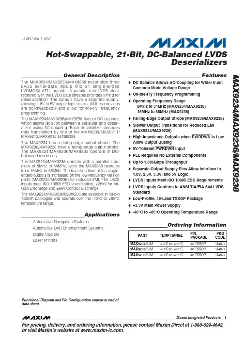
General DescriptionThe MAX9234/MAX9236/MAX9238 deserialize three LVDS serial-data inputs into 21 single-ended LVCMOS/LVTTL outputs. A parallel-rate LVDS clock received with the LVDS data streams provides timing for deserialization. The outputs have a separate supply,allowing 1.8V to 5V output logic levels. All these devices are hot-swappable and allow “on-the-fly” frequency programming.The MAX9234/MAX9236/MAX9238 feature DC balance,which allows isolation between a serializer and deseri-alizer using AC-coupling. Each deserializer decodes data transmitted by one of the MAX9209/MAX9211/MAX9213/MAX9215 serializers.The MAX9234 has a rising-edge output strobe. The MAX9236/MAX9238 have a falling-edge output strobe.The MAX9234/MAX9236/MAX9238 operate in DC-balanced mode only.The MAX9234/MAX9236 operate with a parallel input clock of 8MHz to 34MHz, while the MAX9238 operates from 16MHz to 66MHz. The transition time of the single-ended outputs is increased on the low-frequency version parts (MAX9234/MAX9236) for reduced EMI. The LVDS inputs meet ISO 10605 ESD specification, ±25kV for Air-Gap Discharge and ±8kV Contact Discharge.The MAX9234/MAX9236/MAX9238 are available in 48-pin TSSOP packages and operate over the -40°C to +85°C temperature range.ApplicationsAutomotive Navigation Systems Automotive DVD Entertainment Systems Digital Copiers Laser PrintersFeatures♦DC Balance Allows AC-Coupling for Wider Input Common-Mode Voltage Range ♦On-the-Fly Frequency Programming ♦Operating Frequency Range8MHz to 34MHz (MAX9234/MAX9236)16MHz to 66MHz (MAX9238)♦Falling-Edge Output Strobe (MAX9236/MAX9238)♦Slower Output Transitions for Reduced EMI (MAX9234/MAX9236)♦High-Impedance Outputs when PWRDWN Is Low Allow Output Busing ♦5V-Tolerant PWRDWN Input♦PLL Requires No External Components ♦Up to 1.386Gbps Throughput♦Separate Output Supply Pins Allow Interface to 1.8V, 2.5V, 3.3V, and 5V Logic ♦LVDS Inputs Meet ISO 10605 ESD Requirements ♦LVDS Inputs Conform to ANSI TIA/EIA-644 LVDS Standard ♦Low-Profile, 48-Lead TSSOP Package ♦+3.3V Main Power Supply♦-40°C to +85°C Operating Temperature RangeMAX9234/MAX9236/MAX9238Hot-Swappable, 21-Bit, DC-Balanced LVDSDeserializers________________________________________________________________Maxim Integrated Products 1Ordering Information19-3641; Rev 1; 10/07For pricing, delivery, and ordering information,please contact Maxim Direct at 1-888-629-4642,or visit Maxim’s website at .Functional Diagram and Pin Configuration appear at end of data sheet.M A X 9234/M A X 9236/M A X 9238Hot-Swappable, 21-Bit, DC-Balanced LVDS Deserializers 2_______________________________________________________________________________________ABSOLUTE MAXIMUM RATINGSDC ELECTRICAL CHARACTERISTICS(V CC = +3.0V to +3.6V, V CCO = +3.0V to +5.5V, PWRDWN = high, differential input voltage ⏐V ID ⏐= 0.05V to 1.2V, input common-mode voltage V CM = ⏐V ID /2⏐to 2.4V - ⏐V ID /2⏐, T A = -40°C to +85°C, unless otherwise noted. Typical values are at V CC = V CCO =+3.3V, ⏐V ID ⏐= 0.2V, V CM = 1.25V, T A = +25°C.) (Notes 1, 2)Stresses beyond those listed under “Absolute Maximum Ratings” may cause permanent damage to the device. These are stress ratings only, and functional operation of the device at these or any other conditions beyond those indicated in the operational sections of the specifications is not implied. Exposure to absolute maximum rating conditions for extended periods may affect device reliability.V CC to GND...........................................................-0.5V to +4.0V V CCO to GND.........................................................-0.5V to +6.0V RxIN_, RxCLK IN_ to GND ....................................-0.5V to +4.0V PWRDWN to GND....................................................-0.5V to 6.0V RxOUT_, RxCLK OUT to GND................-0.5V to (V CCO + 0.5V)Continuous Power Dissipation (T A = +70°C)48-Pin TSSOP (derate 16mW/°C above +70°C).......1282mW Storage Temperature Range.............................-65°C to +150°C Junction Temperature......................................................+150°CESD ProtectionHuman Body Model (R D = 1.5k Ω, C S = 100pF)All Pins to GND..................................………………….±5kV IEC 61000-4-2 (R D = 330Ω, CS = 150pF)Contact Discharge (RxIN_, RxCLK IN_) to GND .........±8kV Air-Gap Discharge (RxIN_, RxCLK IN_) to GND .......±15kV ISO 10605 (R D = 2k Ω, C S = 330pF)Contact Discharge (RxIN_, RxCLK IN_) to GND ........±8kV Air Discharge (RxIN_, RxCLK IN_) to GND ...............±25kV Lead Temperature (soldering, 10s).................................+300°CMAX9234/MAX9236/MAX9238Hot-Swappable, 21-Bit, DC-Balanced LVDSDeserializers_______________________________________________________________________________________3DC ELECTRICAL CHARACTERISTICS (continued)(V CC = +3.0V to +3.6V, V CCO = +3.0V to +5.5V, PWRDWN = high, differential input voltage ⏐V ID ⏐= 0.05V to 1.2V, input common-mode voltage V CM = ⏐V ID /2⏐to 2.4V - ⏐V ID /2⏐, T A = -40°C to +85°C, unless otherwise noted. Typical values are at V CC = V CCO =+3.3V, ⏐V ID ⏐= 0.2V, V CM = 1.25V, T A = +25°C.) (Notes 1, 2)M A X 9234/M A X 9236/M A X 9238Hot-Swappable, 21-Bit, DC-Balanced LVDS Deserializers 4_______________________________________________________________________________________TH TL Note 2:Maximum and minimum limits overtemperature are guaranteed by design and characterization. Devices are productiontested at T A = +25°C.Note 3:AC parameters are guaranteed by design and characterization, and are not production tested. Limits are set at ±6 sigma.Note 4:C L includes probe and test jig capacitance.Note 5:RCIP is the period of RxCLK IN. RCOP is the period of RxCLK OUT. RCIP = RCOP.Note 6:RSKM measured with ≤150ps cycle-to-cycle jitter on RxCLK IN.AC ELECTRICAL CHARACTERISTICS(V CC = V CCO = +3.0V to +3.6V, 100mV P-P at 200kHz supply noise, C L = 8pF, PWRDWN = high, differential input voltage ⏐V ID ⏐=0.1V to 1.2V, input common mode voltage V CM = ⏐V ID /2⏐to 2.4V - ⏐V ID /2⏐, T A = -40°C to +85°C, unless otherwise noted. Typical values are at V CC = V CCO = +3.3V, ⏐V ID ⏐= 0.2V, V CM = 1.25V, T A = +25°C.) (Notes 3, 4, 5)MAX9234/MAX9236/MAX9238Hot-Swappable, 21-Bit, DC-Balanced LVDSDeserializers_______________________________________________________________________________________5MAX9234/MAX9236WORST-CASE PATTERN AND PRBS SUPPLY CURRENT vs. FREQUENCYFREQUENCY (MHz)S U P P L Y C U R R E N T (m A )30252015104030506070809010054035MAX9238WORST-CASE PATTERN AND PRBS SUPPLY CURRENT vs. FREQUENCYFREQUENCY (MHz)S U P P L Y C U R R E N T (m A )60504030206040801001201401601801070MAX9234/MAX9236RxOUT TRANSITION TIMEvs. OUTPUT SUPPLY VOLTAGE (V CCO )OUTPUT SUPPLY VOLTAGE (V)O U T P U T T R A N S I T I O N T I M E (n s )4.54.03.53.012345672.55.0MAX9238RxOUT TRANSITION TIMEvs. OUTPUT SUPPLY VOLTAGE (V CCO )OUTPUT SUPPLY VOLTAGE (V)O U T P U T T R A N S I T I O N T I M E (n s )4.54.03.53.0123452.55.0Typical Operating Characteristics(V CC = V CCO = +3.3V, C L = 8pF, PWRDWN = high, differential input voltage ⏐V ID ⏐= 0.2V, input common-mode voltage V CM = 1.2V,T A = +25°C, unless otherwise noted.)M A X 9234/M A X 9236/M A X 9238Hot-Swappable, 21-Bit, DC-Balanced LVDS Deserializers 6_______________________________________________________________________________________Pin DescriptionMAX9234/MAX9236/MAX9238Hot-Swappable, 21-Bit, DC-Balanced LVDSDeserializers_______________________________________________________________________________________7Detailed DescriptionThe MAX9234/MAX9236 operate at a parallel clock fre-quency of 8MHz to 34MHz. The MAX9238 operates at a parallel clock frequency of 16MHz to 66MHz. The tran-sition times of the single-ended outputs are increased on the MAX9234/MAX9236 for reduced EMI.DC BalanceData coding by the MAX9209/MAX9211/MAX9213/MAX9215 serializers (which are companion devices to the MAX9234/MAX9236/MAX9238 deserializers) limits the imbalance of ones and zeros transmitted on each channel. If +1 is assigned to each binary 1 transmitted and -1 is assigned to each binary 0 transmitted, the varia-tion in the running sum of assigned values is called the digital sum variation (DSV). The maximum DSV for the data channels is 10. At most, 10 more zeros than ones,or 10 more ones than zeros, are transmitted. The maxi-mum DSV for the clock channel is five. Limiting the DSV and choosing the correct coupling capacitors maintains differential signal amplitude and reduces jitter due to droop on AC-coupled links.To obtain DC balance on the data channels, the serial-izer parallel data is inverted or not inverted, depending on the sign of the digital sum at the word boundary.Two complementary bits are appended to each group of 7 parallel input data bits to indicate to the MAX9234/MAX9236/MAX9238 deserializers whether the data bits are inverted (see Figure 9). The deserializer restores the original state of the parallel data. The LVDS clock signal alternates duty cycles of 4/9 and 5/9, which maintain DC balance.AC-Coupling BenefitsBit errors experienced with DC-coupling can be elimi-nated by increasing the receiver common-mode voltage range by AC-coupling. AC-coupling increases the com-mon-mode voltage range of an LVDS receiver to nearly the voltage rating of the capacitor. The typical LVDS dri-ver output is 350mV centered on an offset voltage of 1.25V, making single-ended output voltages of 1.425V and 1.075V. An LVDS receiver accepts signals from 0 to 2.4V, allowing approximately ±1V common-mode differ-ence between the driver and receiver on a DC-coupledCommon-mode voltage differences may be due to ground potential variation or common-mode noise. If there is more than ±1V of difference, the receiver is not guaranteed to read the input signal correctly and may cause bit errors. AC-coupling filters low-frequency ground shifts and common-mode noise and passes high-frequency data. A common-mode voltage differ-ence up to the voltage rating of the coupling capacitor (minus half the differential swing) is tolerated. DC-bal-anced coding of the data is required to maintain the dif-ferential signal amplitude and limit jitter on an AC-coupled link. A capacitor in series with each output of the LVDS driver is sufficient for AC-coupling.However, two capacitors—one at the serializer output and one at the deserializer input—provide protection in case either end of the cable is shorted to a high voltage.Figure 1. LVDS Input CircuitM A X 9234/M A X 9236/M A X 9238Hot-Swappable, 21-Bit, DC-Balanced LVDS Deserializers 8_______________________________________________________________________________________Figure 4. LVDS Receiver Input Skew MarginFigure 5a. MAX9234 Output Setup/Hold and High/Low TimesFigure 5b. MAX9236/MAX9238 Output Setup/Hold and High/Low TimesFigure 6a. MAX9234 Clock-IN to Clock-OUT DelayFigure 6b. MAX9236/MAX9238 Clock-IN to Clock-OUT DelayFigure 7. Phase-Locked Loop Set TimeMAX9234/MAX9236/MAX9238Hot-Swappable, 21-Bit, DC-Balanced LVDSDeserializers_______________________________________________________________________________________9MAX9234/MAX9236/MAX9238 vs.MAX9210/MAX9220/MAX9222The MAX9234/MAX9236/MAX9238 operate in DC-bal-ance mode only. Pinouts are the same as the MAX9210/MAX9220/MAX9222 except that pin 6 on the MAX9234/MAX9236/MAX9238 is no connect (N.C.). DC balance allows AC-coupling with series capacitors. The MAX9234/MAX9236/MAX9238 are hot-swappable and the input frequency can be changed on the fly, but oth-erwise the specifications and functionality are the same as the MAX9210/MAX9220/MAX9222 operating in DC-balance mode. See Table 1.Applications InformationSelection of AC-Coupling CapacitorsVoltage droop and the DSV of transmitted symbols cause signal transitions to start from different voltage levels. Because the transition time is finite, starting the signal transition from different voltage levels causes timing jitter. The time constant for an AC-coupled link needs to be chosen to reduce droop and jitter to an acceptable level.The RC network for an AC-coupled link consists of the LVDS receiver termination resistor (R T ), the LVDS driver output resistor (R O ), and the series AC-coupling capac-itors (C). The RC time constant for two equal-value series capacitors is (C x (R T + R O )) / 2 (Figure 10). The RC time constant for four equal-value series capacitors is (C x (R T + R O )) / 4 (Figure 11).R T is required to match the transmission line imped-ance (usually 100Ω) and R O is determined by the LVDS driver design (the minimum differential output resis-tance of 78Ωfor the MAX9209/MAX9211/MAX9213/MAX9215 serializers is used in the following example).This leaves the capacitor selection to change the sys-tem time constant.Figure 9. Deserializer Serial InputFigure 8. Power-Down DelayM A X 9234/M A X 9236/M A X 9238Hot-Swappable, 21-Bit, DC-Balanced LVDS DeserializersFigure 10. Two Capacitors per Link, AC-CoupledMAX9234/MAX9236/MAX9238Hot-Swappable, 21-Bit, DC-Balanced LVDSDeserializers______________________________________________________________________________________11In the following example, the capacitor value for a droop of 2% is calculated. J itter due to this droop is then calculated assuming a 1ns transition time:C = - (2 x t B x DSV) / (ln (1 - D) x (R T + R O )) (Eq 1)where:C = AC-coupling capacitor (F).t B = bit time (s).DSV = digital sum variation (integer).ln = natural log.D = droop (% of signal amplitude).R T = termination resistor (Ω).R O = output resistance (Ω).Equation 1 is for two series capacitors (Figure 10). The bit time (t B ) is the period of the parallel clock divided by 9. The DSV is 10. See equation 3 for four series capaci-tors (Figure 11).The capacitor for 2% maximum droop at 8MHz parallel rate clock is:C = - (2 x t B x DSV) / (ln (1 - D) x (R T + R O ))C = - (2 x 13.9ns x 10) / (ln (1 - 0.02) x (100Ω+ 78Ω))C = 0.0773µFJ itter due to droop is proportional to the droop and transition time:t J = t T x D (Eq 2)where:t J = jitter (s).t T = transition time (s) (0 to 100%).D = droop (% of signal amplitude).Jitter due to 2% droop and assumed 1ns transition time is:t J = 1ns x 0.02t J = 20psThe transition time in a real system depends on the fre-quency response of the cable driven by the serializer.The capacitor value decreases for a higher frequency parallel clock and for higher levels of droop and e high-frequency, surface-mount ceramic capacitors.Equation 1 altered for four series capacitors (Figure 11) is:C = - (4 x t B x DSV) / (ln (1 - D) x (R T + R O )) (Eq 3)Input Bias and Frequency DetectionThe inverting and noninverting LVDS inputs are internally connected to +1.2V through 42k Ω(min) to provide bias-ing for AC-coupling (Figure 1).A frequency-detection circuit on the clock input detects when the input is not switching, or is switching at low frequency. In this case,all outputs are driven low. To prevent switching due to noise when the clock input is not driven, bias the clock input to differential +15mV by connecting a 10k Ω±1%pullup resistor between the noninverting input and V CC ,and a 10k Ω±1% pulldown resistor between the invert-ing input and ground. These bias resistors, along with the 100Ω±1% tolerance termination resistor, provide +15mV of differential input.Unused LVDS Data InputsAt each unused LVDS data input, pull the inverting input up to V CC using a 10k Ωresistor, and pull the noninverting input down to ground using a 10k Ωresistor. Do not con-nect a termination resistor. The pullup and pulldown resis-tors drive the corresponding outputs low and prevent switching due to noise.PWRDWNDriving PWRDWN low puts the outputs in high imped-ance, stops the PLL, and reduces supply current to 50µA or less. Driving PWRDWN high drives the outputs low until the PLL locks. The outputs of two deserializers can be bused to form a 2:1 mux with the outputs con-trolled by PWRDWN . Wait 100ns between disabling one deserializer (driving PWRDWN low) and enabling the second one (driving PWRDWN high) to avoid con-tention of the bused outputs.Input Clock and PLL Lock TimeThere is no required timing sequence for the applica-tion or reapplication of the parallel rate clock (RxCLK IN) relative to PWRDWN , or to a power-supply ramp for proper PLL lock. The PLL lock time is set by an internal counter. The maximum time to lock is 32,800 clock periods. Power and clock should be stable to meet the lock-time specification. When the PLL is locking, the outputs are low.Power-Supply BypassingThere are separate on-chip power domains for digital circuits, outputs, PLL, and LVDS inputs.Bypass each V CC , V CCO , PLL V CC , and LVDS V CC pin with high-fre-quency, surface-mount ceramic 0.1µF and 0.001µF capacitors in parallel as close to the device as possi-ble, with the smallest value capacitor closest to the supply pin.Cables and ConnectorsInterconnect for LVDS typically has a differential imped-ance of 100Ω. Use cables and connectors that have matched differential impedance to minimize impedance discontinuities.Twisted-pair and shielded twisted-pair cables offer superior signal quality compared to ribbon cable and tend to generate less EMI due to magnetic field cancel-ing effects. Balanced cables pick up noise as common mode, which is rejected by the LVDS receiver.M A X 9234/M A X 9236/M A X 9238Hot-Swappable, 21-Bit, DC-Balanced LVDS Deserializers 12______________________________________________________________________________________Board LayoutKeep the LVTTL/LVCMOS outputs and LVDS input sig-nals separated to prevent crosstalk. A four-layer PC board with separate layers for power, ground, LVDS inputs, and digital signals is recommended.ESD ProtectionThe MAX9234/MAX9236/MAX9238 ESD tolerance is rated for IEC 61000-4-2 Human Body Model and ISO 10605 standards. IEC 61000-4-2 and ISO 10605 specifiy ESD tolerance for electronic systems. The Human Body Model discharge components are C S = 100pF and R D =1.5k Ω(Figure 12). For the Human Body Model, all pins are rated for ±5kV contact discharge. The ISO 10605 dis-charge components are C S = 330pF and R D = 2k Ω(Figure 13). For ISO 10605, the LVDS outputs are rated for ±8kV contact and ±25kV air discharge. The IEC 61000-4-2 discharge components are C S = 150pF and R D = 330Ω(Figure 14). For IEC 61000-4-2, the LVDS inputs are rated for ±8kV Contact Discharge and ±15kV Air-Gap Discharge.5V Tolerant InputPWRDWN is 5V tolerant and is internally pulled down to GND.Skew Margin (RSKM)Skew margin (RSKM) is the time allowed for degrada-tion of the serial data sampling setup and hold times by sources other than the deserializer. The deserializer sampling uncertainty is accounted for and does not need to be subtracted from RSKM. The main outside contributors of jitter and skew that subtract from RSKM are interconnect intersymbol interference, serializer pulse position uncertainty, and pair-to-pair path skew.V CCO Output Supply and Power DissipationThe outputs have a separate supply (V CCO ) for interfacing to systems with 1.8V to 5V nominal input-logic levels. The DC Electrical Characteristics table gives the maximum supply current for V CCO = 3.6V with 8pF load at several switching frequencies with all outputs switching in the worst-case switching pattern. The approximate incremen-tal supply current for V CCO other than 3.6V with the same 8pF load and worst-case pattern can be calculated using:I I = C T V I 0.5f C x 21 (data outputs)+ C T V I f C x 1 (clock output)where:I I = incremental supply current.C T = total internal (C INT ) and external (C L ) load capaci-tance.V I = incremental supply voltage.f C = output clock-switching frequency.The incremental current is added to (for V CCO >3.6V)or subtracted from (for V CCO <3.6V) the DC Electrical Characteristics table maximum supply current. The internal output buffer capacitance is C INT = 6pF. The worst-case pattern-switching frequency of the data out-puts is half the switching frequency of the output clock.In the following example, the incremental supply current is calculated for V CCO = 5.5V, f C = 34MHz, and C L = 8pF:V I = 5.5V - 3.6V = 1.9VC T = C INT + C L = 6pF + 8pF = 14pFFigure 13. ISO 10605 Contact Discharge ESD Test CircuitFigure 12. Human Body ESD Test CircuitFigure 14. IEC 61000-4-2 Contact Discharge ESD Test CircuitMAX9234/MAX9236/MAX9238Hot-Swappable, 21-Bit, DC-Balanced LVDSDeserializers______________________________________________________________________________________13where:I I = C T V I 0.5F C x 21 (data outputs) + C T V I f C x 1 (clock output).I I = (14pF x 1.9V x 0.5 x 34MHz x 21) + (14pF x 1.9V x 34MHz).I I = 9.5mA + 0.9mA = 10.4mA.The maximum supply current in DC-balanced mode for V CC = V CCO = 3.6V at f C = 34MHz is 106mA (from the DC Electrical Characteristics table). Add 10.4mA to get the total approximate maximum supply current at V CCO = 5.5V and V CC = 3.6V.If the output supply voltage is less than V CCO = 3.6V,the reduced supply current can be calculated using the same formula and method.At high switching frequency, high supply voltage, and high capacitive loading, power dissipation can exceed the package power-dissipation rating. Do not exceed the maximum package power-dissipation rating. See the Absolute Maximum Ratings for maximum package power-dissipation capacity and temperature derating.Rising- or Falling-Edge Output StrobeThe MAX9234 has a rising-edge output strobe, which latches the parallel output data into the next chip on the rising edge of RxCLK OUT. The MAX9236/MAX9238have a falling-edge output strobe, which latches the parallel output data into the next chip on the falling edge of RxCLK OUT. The deserializer output strobe polarity does not need to match the serializer input strobe polarity. A deserializer with rising- or falling-edge output strobe can be driven by a serializer with a rising-edge input strobe.Pin ConfigurationChip InformationMAX9234 TRANSISTOR COUNT: 14,104MAX9236 TRANSISTOR COUNT: 14,104MAX9238 TRANSISTOR COUNT: 14,104PROCESS: CMOSM A X 9234/M A X 9236/M A X 9238Hot-Swappable, 21-Bit, DC-Balanced LVDS Deserializers 14______________________________________________________________________________________Package Information(The package drawing(s) in this data sheet may not reflect the most current specifications. For the latest package outline information,go to /packages .)MAX9234/MAX9236/MAX9238Hot-Swappable, 21-Bit, DC-Balanced LVDSDeserializersMaxim cannot assume responsibility for use of any circuitry other than circuitry entirely embodied in a Maxim product. No circuit patent licenses are implied. Maxim reserves the right to change the circuitry and specifications without notice at any time.Maxim Integrated Products, 120 San Gabriel Drive, Sunnyvale, CA 94086 408-737-7600 ____________________15©2007 Maxim Integrated Productsis a registered trademark of Maxim Integrated Products, Inc.Revision History。