HCF4049UB
- 格式:pdf
- 大小:119.95 KB
- 文档页数:9
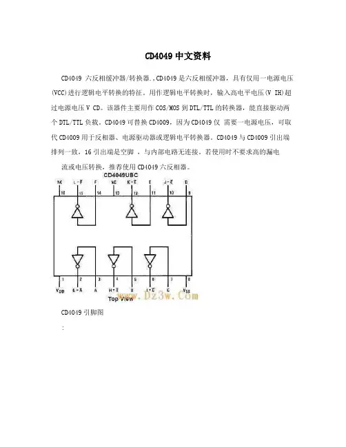
1/9March 2004sPROPAGATION DELAY TIME:t PD =40ns (TYP .)at V DD =10V C L =50pF s HIGH TO LOW LEVEL LOGIC CONVERSION sHIGH "SINK"AND "SOURCE"CURRENT CAPABILITYsQUIESCENT CURRENT SPECIFIED UP TO 20Vs 5V,10V AND 15V PARAMETRIC RATINGS sINPUT LEAKAGE CURRENTI I =100nA (MAX)AT V DD =18V T A =25°C s100%TESTED FOR QUIESCENT CURRENTDESCRIPTIONThe HCF4049UB is a monolithic integrated circuit fabricated in Metal Oxide Semiconductor technology available in DIP and SOP packages.It is an inverting Hex Buffer/Converter and feature logic level conversions using only one supply voltage (V DD ).The input high level signal (V IH )can exceed the V DD supply voltage when these devices are usedfor logic level conversions.This device is intended for use as CMOS to DTL/TTL converters and can drive directly two DTL/TTL loads (V DD =5V,V OL ≤0.4V and I OL ≤ 3.2mA.HCF4049UBHEX BUFFER/CONVERTER(INVERTING)PIN CONNECTIONORDER CODESPACKAGE TUBE T &RDIP HCF4049UBEY SOPHCF4049UBM1HCF4049UM013TRHCF4049UB2/9INPUT EQUIVALENT CIRCUITPIN DESCRIPTIONTRUTH TABLEABSOLUTE MAXIMUM RATINGSAbsolute Maximum Ratings are those values beyond which damage to the device may occur.Functional operation under these conditions is not implied.All voltage values are referred to V SS pin voltage.RECOMMENDED OPERATING CONDITIONSPIN N°SYMBOLNAME AND FUNCTION 3,5,7,9,11,14A,B,C,D,E,FData Inputs 2,4,6,10,12,15G,H,I,J,K,L Data Outputs 13,16NCNot Connected8V SS Negative Supply Voltage 1V DDPositive Supply VoltageINPUTS OUTPUTS A,B,C,D,E,FG,H,I,J,K,LL H HLSymbol ParameterValue Unit V DD Supply Voltage -0.5to +22V V I DC Input Voltage -0.5to +18V I I DC Input Current±10mA P D Power Dissipation per Package200mW Power Dissipation per Output Transistor 100mW T op Operating Temperature -55to +125°C T stgStorage Temperature-65to +150°CSymbol ParameterValue Unit V DD Supply Voltage 3to 20V V I Input Voltage-0.5to 15V V T opOperating Temperature-55to 125°CHCF4049UB3/9DC SPECIFICATIONSThe Noise Margin for both "1"and "0"level is:1V min.with V DD =5V,2V min.with V DD =10V,2.5V min.with V DD =15VSymbolParameterTest ConditionValue UnitV I (V)V O (V)|I O |(µA)V DD (V)T A =25°C -40to 85°C -55to 125°C Min.Typ.Max.Min.Max.Min.Max.I LQuiescent Current0/550.0213030µA0/10100.02260600/15150.024*******/20200.0420600600V OHHigh Level Output Voltage0/5<15 4.95 4.95 4.95V0/10<1109.959.959.950/15<11514.9514.9514.95V OLLow Level Output Voltage 5/0<150.050.050.05V10/0<1100.050.050.0515/0<1150.050.050.05V IHHigh Level Input Voltage 0.5/4.5<15444V1/9<1108881.5/13.5<115121212V ILLow Level Input Voltage 4.5/0.5<15111V9/1<11022213.5/1.5<115333I OHOutput Drive Current0/5 2.5<15-1.25-6.4-0.42-0.42mA0/5 4.6<15-0.51-1.6-0.38-0.380/109.5<110-1.25-3.6-1-10/1513.5<115-3.75-12-3-3I OLOutput Sink Current0/50.4<15 3.2 6.4 2.6 2.6mA 0/100.5<110816 6.6 6.60/15 1.5<11524481919I I Input Leakage Current0/18Any Input 18±10-5±0.1±1±1µA C IInput CapacitanceAny Input57.5pFHCF4049UB4/9DYNAMIC ELECTRICAL CHARACTERISTICS (T amb =25°C,C L =50pF,R L =200K Ω,t r =t f =20ns)(*)Typical temperature coefficient for all V DD value is 0.3%/°C.TEST CIRCUITL R L =200K ΩR T =Z OUT of pulse generator (typically 50Ω)Symbol ParameterTest ConditionValue (*)UnitV DD (V)V I (V)Min.Typ.Max.t TLHOutput Transition Time5580160ns 1010408015153060t THLOutput Transition Time553060ns1010204015151530t PLHPropagation Delay Time5560120ns101032655104590151525505154590t PHLPropagation Delay Time553265ns101020405101530151515305151020HCF4049UB5/9WAVEFORM:PROPAGATION DELAY TIMES (f=1MHz;50%dutycycle)HCF4049UB Information furnished is believed to be accurate and reliable. However, STMicroelectronics assumes no responsibility for the consequences of use of such information nor for any infringement of patents or other rights of third parties which may result from its use. No license is granted by implication or otherwise under any patent or patent rights of STMicroelectronics. Specifications mentioned in this publication are subject to change without notice. This publication supersedes and replaces all information previously supplied. STMicroelectronics products are not authorized for use as critical components in life support devices or systems without express written approval of STMicroelectronics.The ST logo is a registered trademark of STMicroelectronicsAll other names are the property of their respective owners© 2004 STMicroelectronics - All Rights ReservedSTMicroelectronics GROUP OF COMPANIESAustralia - Belgium - Brazil - Canada - China - Czech Republic - Finland - France - Germany - Hong Kong - India - Israel - Italy - Japan - Malaysia - Malta - Morocco - Singapore - Spain - Sweden - Switzerland - United Kingdom - United States.9/9。