数据采集板卡指标
- 格式:pdf
- 大小:575.94 KB
- 文档页数:12


⏹ 系统需求系统由测试台和测试柜两部分组成。
测试柜:主要由电路控制箱盒工控机构成。
工控机包含PCI-1710HG ,PCI-1760,PCL-839等三块卡。
PCI-1760为8路继电器输出卡,用来控制测试电路的档位切换,电源的切换,以及步进电机驱动器的启动。
PCI-1710HG 为高增益AD 采集卡用来采集控制回路的反馈电压,获取力矩器在不同角度下的力矩。
PCL-839用来控制步进电机驱动器,使力矩器力矩器定子转动到合适的角度。
测试台包括以静压空气轴承为支撑的测试主轴和梁体组件(6)组成活动部分:以角位移传感器(3),音圈力矩器(4),电子转换放大器组成的力矩反馈电气部分;由带动被测电机定子座(7)旋转、定位用的步进电机与涡轮蜗杆和步进电机等组成的传动机构部分⏹ 系统描述力矩测试原理当梁体组件受到被测电机的转矩Ma 作用时,它立刻偏离原来平衡位置。
其偏移角α的讯号经位移传感器、电子放大器、在音圈力矩器回路中产生一个反馈电流If ,并且产生一个反馈转矩Mf ,此转矩与被测电机转矩Ma 相比较,实现模拟量加矩再平衡。
通过PCI-1710GH 取出与反馈电流If成正比的采样标准电阻端电压Ur ,就是与被测电机转矩成正比的数值。
案例名称:基于研华ATE 设备的高精度力矩测试仪系统行业分类:ATE (工厂自动化)地点:软件实施软件部分使用DELPHI6.0开发应用程序。
整个软件包括数据采集、数据动态显示、步进电机驱动、数据后期分析处理,数据库操作、测试报表输出等几部分。
1、测试流程控制模块。
主要通过操作PCI-1760,PCL-839来完成。
根据测试大纲的步骤依次操作继电器的切换。
通过控制步进电机使力矩器转动到规定的测试点。
这部分软件操作通过使用研华提供的动态链接库很方便的实现,避免了直接对板卡端口的操作,大大简化了编程开发。
测试流程如下2、模拟量采集存储、数据实时显示模块是自动测试系统比较重要的环节。
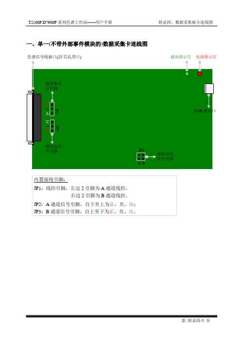
T2100P/D7900P 系列色谱工作站——用户手册 附录四、数据采集板卡连线图
--- 第 附录四-1 页 ---
一、单一
(不带外部事件模块的)数据采集卡连线图
附录四、数据采集板卡连线图T2100P/D7900P系列色谱工作站——用户手册二、集成(带外部事件模块的)数据采集卡连线图
【注意】
1)依据输出电压的不同,共有直流和交流两种制式的外部事件模块;直流制式
又通常分为5V、12V和24V。
2)输入电源必须与该模块的输出制式及电压值相匹配,严禁混淆。
3)有源输出可直接驱动制式和电压与之匹配的电磁阀,且带限流功能。
4)必须认准输入电源极性,确保正接正,负接负,切忌接反。
5)若带电情况下接入色谱信号,务必先地接地,再正接正、负接负。
6)建议将色谱信号直接连入内置引脚(注意极性匹配),取代25芯外置式连接。
---第附录四-2 页---。


模拟量差分输入方式的应用指南适用范围本应用手册中的内容适用于PCM系列数据采集板卡中PCM-8208BT、PCM-8208BS隔离模拟量输入板卡。
对于非隔离的板卡PCM-8308BS也可以参考其接线方式应用于现场。
1.PCM-8208BT、PCM-8208BS数据采集板卡主要参数PCM系列数据采集板卡为支持PC/104总线接口的数据采集板卡。
PCM-8208BT数据采集板卡的主要参数如下:●隔离模拟量输入●16路单端或者8路差分隔离输入(可配置)●输入端口隔离电压:1000VDC●输入电压范围:±0.625V、±1.25V、±2.5V、±5V、±10V●ADC分辨率:12bit●最大48K转换速率●板载的I/O保护和过滤PCM-8208BS数据采集板卡的主要参数如下:●隔离模拟量输入●16路单端或者8路差分隔离输入(可配置)●输入端口隔离电压:1000VDC●输入电压范围:±0.625V、±1.25V、±2.5V、±5V、±10V●ADC分辨率:16bit●最大48K转换速率●板载的I/O保护和过滤2. 接线端子板ZUDB-3100APCM系列数据采集板卡可以配合接线端子板ZUDB-3100A使用,方便用户的现场接线和安装,数据采集板卡与ZUDB-3100A端子板组合能够快速、方便的组建工业数据采集系统。
对于模拟量输入板卡,ZUDB-3100A提供前端功能电路,通过选焊部分电阻电容,可以实现模拟单端/差分信号滤波,分压,4~20mA电流环转换成电压等功能。
本应用手册中介绍的接线方法配合接线端子板ZUDB-3100A使用会更加便利。
模拟量输入接线方式介绍PCM系列数据采集板卡提供两种类型的模拟量输入的接线方式:单端连接方式和差分连接方式。
1. 单端连接方式单端连接方式对每个通道来说只有一根信号线,以及一根共同的地线构成回路。
采集卡的选择和主要参数图像采集卡是将视频信号经过AD转换后,将视频转换成电脑可使用的数字格式,经过PCI总线实时传到内存和显存。
在采集过程中,由于采集卡传送数据采用PCI Master Burst方式,图像传送速度高达40MB/S,可实现摄像机图像到计算机内存的可靠实时传送,并且几乎不占用CPU时间,留给CPU更多的时间去做图像的运算与处理。
一、采集卡基本原理采集卡有多种种类、规格。
但尽管其设计和特性不同,大多数采集卡的基本原理相同。
近年来,数字视频产品取得了显著发展。
数字视频产品通常需要对动态图像进行实时采集和处理,因此产品性能受图像采集卡的性能影响很大。
由于早期图像采集卡以帧存为核心,处理图像时需读写帧存,对于动态画面还需“冻结”图像,同时由于数据传输速率的限制,因此图像处理速度缓慢。
90年代初,INTEL公司提出了PCI(Peripheral Component Interconnect)局部总线规范。
PCI总线数据传宽度为32/64位,允许系统设备直接或间接连接其上,设备间可通过局部总线完成数据的快速传送,从而较好地解决了数据传输的瓶颈问题。
由于PCI总线的高速度,使A/D转换以后的数字视频信号只需经过一个简单的缓存器即可直接存到计算机内存,供计算机进行图像处理也可将采集到内存的图像信号传送到计算机显示卡显示;甚至可将A/D输出的数字视频信号经PCI总线直接送到显示卡,在计算机终端上实时显示活动图像。
数据锁存器代替了帧存储器,这个缓存是一片容量小、控制简单的先进先出(FIFO)存储器,起到图像卡向PCI总线传送视频数据时的速度匹配作用。
将图像卡插在计算机的PCI插槽中,与计算机内存、CPU、显示卡等之间形成调整数据传送。
由于PCI总线的上述优点,许多图像板卡公司陆续推出了基于PCI总线的图像采集卡,另外还有PC104 plus、Compact PCI等总线形式。
二、与图像采集卡相关技术名词1、DMADMA( Direct Memory Access)是一种总线控制方式,它可取代CPU对总线的控制,在数据传输时根据数据源和目的的逻辑地址和物理地址映射关系,完成对数据的存取,这样可以大大减轻数据传输时CPU的负担。
具体来说,这种设计分两部分:数据采集部分和数据处理部分。
数据采集就是利用LabVIEW的驱动程序对数据采集卡进行设置并使其按设置工作,进行数据的采集;数据处理则是将采集到的数据送至计算机进行运算处理等等。
对于初学者,可先从第二部分开始。
将实际的数据采集先用LabVIEW自带的数组或者波形函数来代替,着重设计数据处理的软件部分。
这部分可以包括:滤波、数据存储、数据读取、波形显示、波形分析处理(如傅立叶变换、谱密度计算等等)。
这些在LabVIEW中都有集成的函数模块,也就是VI,只要对每个VI的输入输出设置正确就好。
当软件部分设计完成后,再设计数据采集部分。
这是软硬件结合的部分。
既要对所用的数据采集卡的参数和工作方式有充分的正确的认识,又要对如果利用LabVIEW驱动采集卡掌握。
一般来说采集卡都带有LabVIEW的驱动,只要参看数据采集卡的使用说明(PDF),就可以掌握了。
选择好数据采集卡后,将该采集卡的驱动光盘放入计算机并按其指示进行安装,则其驱动模块将装入原LabVIEW软件中,然后和第一步的软件编程一样,对驱动所要用的VI的输入输出参数设置正确,编写程序即可。
当两部都做完后,将整个采集系统运行一下,对于设计中存在的疏漏再进行修改。
推荐使用《LadVIEW8.20程序设计从入门到精通(附光盘)》作者:陈锡鸿这本书不错,深入浅出,初学必备~~数据采集(DAQ)基础知识现今,在实验室研究、测试和测量以及工业自动化领域中,绝大多数科研人员和工程师使用配有PCI、PXI/CompactPCI、PCMCIA、USB、IEEE1394、ISA、并行或串行接口的基于PC的数据采集系统。
许多应用使用插入式设备采集数据并把数据直接传送到计算机内存中,而在一些其它应用中数据采集硬件与PC分离,通过并行或串行接口和PC相连。
从基于PC的数据采集系统中获取适当的结果取决于图示一中的各项组成部分:•PC•传感器•信号调理•数据采集硬件•软件本文详细介绍了数据采集系统的各个组成部分,并解释各个部分最重要的准则。
MPS-140801 8通道24位USB信号采集卡MPS-140801是一款高性能的24位采集卡。
MPS-140801具有八路同步采样的电压输入通道,量程为±10V(或按要求提供±5V、±2.5V的版本),输入阻抗1M欧姆(或按要求定制,最高可达100G欧姆)。
每个通道每秒可采集52K样点(从1.5K到52K六档可编程设置)。
采样噪声极低,最佳情况下噪声峰峰值只有0.00004V(满量程的五十万分之一),有效分辨率达21.8bit,信噪比121dB。
MPS-140801支持多卡并联,最多同时连接10块板卡,从而扩展到80个输入通道。
MPS-140801随卡提供外部电源、BNC接头信号线、同步信号传输线和外部启动触发器等配件。
并配有高性能的应用软件,可以在计算机上观察到采集的波形,并把数据实时写入硬盘,在需要的时候对数据进行回放或导出为TXT文本文件。
MPS-140801目前在同类产品中处于领先地位,但价格保持了莫非电子一贯的风格,保持在同性念产品价格的1/3以下。
让客户用最少的投入,获得最好的产品。
在多通道高精度的高端项目中,MPS-140801毫无疑问是最佳的选择。
一、产品简介MPS-140801是一款基于USB总线的高性能信号采集卡。
MPS-140801具有八路大量程、高采样率、低噪声的高性能同步信号采集通道。
每个通道的量程为±10V,采样率高达52.734Ksps,并能保证实时传输到计算机进行显示与分析。
通过高性能ADC和先进的DSP信号处理技术,MPS-140801同时还具有极低的采样噪声,在1.643Ksps采样率下采样噪声峰峰值仅为0.00004V,满量程信号的信噪比高达50万。
多通道、高采样率和低噪声和同步采样使MPS-140801能够满足科研与生产中绝大部分信号采集工程的需要。
MPS-140801采用USB2.0高速总线接口,支持即插即用和热插拔,是便携式系统用户的最佳选择。
NI632x SpecificationsSpecifications listed below are typical at 25°C unless otherwise noted. Refer to the X Series User Manual for more information about NI PCIe-6320/6321/6323 devices.Analog InputNumber of channelsNI 6320/6321..............................8 differential or16single ended NI 6323.......................................16 differential or32single endedADC resolution...............................16 bits DNL................................................No missing codesguaranteed INL..................................................Refer to the AI AbsoluteAccuracy TableSampling rateMaximum...................................250 kS/s single channel,250 kS/s multi-channel(aggregate)Minimum....................................No minimumTiming accuracy.........................50 ppm of sample rate Timing resolution.......................10 nsInput coupling.................................DCInput range......................................±10V, ±5V,±1V,±0.2V Maximum working voltage for analog inputs(signal + common mode)................±11 V of AI GND CMRR (DC to 60 Hz).....................100 dBInput impedanceDevice onAI+ to AI GND......................>10 GΩ in parallelwith100 pFAI– to AI GND......................>10 GΩ in parallelwith100 pFDevice offAI+ to AI GND......................1200 ΩAI– to AI GND.......................1200 ΩInput bias current.............................±100 pACrosstalk (at 100 kHz)Adjacent channels.......................–75 dBNon-adjacent channels................–90 dBSmall signal bandwidth (–3 dB)......700 kHzInput FIFO size................................4,095 samplesScan list memory.............................4,095 entriesData transfers...................................DMA (scatter-gather),programmed I/OOvervoltage protection (AI <0..31>, AI SENSE, AI SENSE2) Device on....................................±25 V for up totwo AI pinsDevice off...................................±15 V for up totwo AI pinsInput current duringovervoltage condition......................±20 mA max/AI pinSettling Time for Multichannel Measurements Accuracy, full scale step, all ranges±90 ppm of step (±6 LSB)..........4 μs convert interval±30 ppm of step (±2 LSB)..........5 μs convert interval±15 ppm of step (±1 LSB)..........7 μs convert intervalAnalog triggers................................NoneTypical Performance GraphsAnalog OutputNumber of channelsNI 6320 0NI 6321 (2)NI 6323 (4)DAC resolution................................16 bits DNL.................................................±1 LSB Monotonicity...................................16 bit guaranteedMaximum update rate1 channel.....................................900 kS/s2 channels...................................840 kS/s per channel3 channels...................................775 kS/s per channel4 channels...................................719 kS/s per channel Timing accuracy..............................50 ppm of sample rate Timing resolution............................10 nsOutput range....................................±10 VOutput coupling...............................DCOutput impedance............................0.2 ΩOutput current drive........................±5 mAOverdrive protection........................±15 VOverdrive current............................15 mAPower-on state.................................±20 mVPower-on/off glitch..........................2 V for 500 ms Output FIFO size.............................8,191 samples sharedamong channels used Data transfers...................................DMA (scatter-gather),programmed I/O AO waveform modes:•Non-periodic waveform•Periodic waveform regeneration mode from onboard FIFO •Periodic waveform regeneration from host buffer including dynamic updateSettling time, full scale step15 ppm (1 LSB)..............................6 μsSlew rate.........................................15 V/μsGlitch energyMagnitude...................................100 mVDuration......................................2.6 μsCalibration (AI and AO)Recommended warm-up time.........15 minutesCalibration interval.........................1 yearNI 632x © National Instruments Corporation 5NI 632x SpecificationsDigital I/O/PFIStatic CharacteristicsNumber of channelsNI 6320/6321..............................24 total,8(P0.<0..7>)16(PFI <0..7>/P1, PFI <8..15>/P2)NI 6323.......................................48 total,32 (P0.<0..31>) 16(PFI <0..7>/P1, PFI <8..15>/P2)Ground reference............................D GND Direction control.............................Each terminalindividually programmable as input or output Pull-down resistor...........................50 k Ω typical,20k Ωminimum Input voltage protection 1.................±20 V on up to two pinsWaveform Characteristics (Port 0Only)Terminals usedNI 6320/6321..............................Port 0 (P0.<0..7>)NI 6323.......................................Port 0 (P0.<0..31>)Port/sample sizeNI 6320/6321..............................Up to 8 bits NI 6323.......................................Up to 32 bits Waveform generation (DO) FIFO....2,047 samples Waveform acquisition (DI) FIFO...255 samplesDO or DI Sample Clockfrequency ........................................0 to 1 MHz, system andbus activity dependent Data transfers..................................DMA (scatter-gather),programmed I/O Digital line filter settings................160 ns, 10.24 μs, 5.12 ms,disablePFI/Port 1/Port 2 FunctionalityFunctionality....................................Static digital input,static digital output, timing input, timing output Timing output sources.....................Many AI, AO, counter,DI, DO timing signals Debounce filter settings...................90ns, 5.12μs, 2.56ms,custom interval, disable; programmable high and low transitions; selectable per inputRecommended Operation ConditionsElectrical Characteristics1 Stresses beyond those listed under Input voltage protection may cause permanent damage to the device.LevelMin Max Input high voltage (V IH ) 2.2 V 5.25 V Input low voltage (V IL )0 V 0.8 V Output high current (I OH )P0.<0..31>PFI <0..15>/P1/P2——–24 mA –16 mA Output low current (I OL )P0.<0..31>PFI <0..15>/P1/P2——24 mA 16 mALevelMin Max Positive-going threshold (VT+)— 2.2 V Negative-going threshold (VT–)0.8 V —Delta VT hysteresis (VT+–VT–)0.2 V —I IL input low current (V in =0V)I IH input high current (V in =5V)——–10 μA 250 μADigital I/O CharacteristicsNI 632x General-Purpose Counter/TimersNumber of counter/timers (4)Resolution.......................................32 bitsCounter measurements....................Edge counting, pulse,pulse width, semi-period,period, two-edgeseparationPosition measurements...................X1, X2, X4 quadratureencoding withChannel Z reloading;two-pulse encoding Output applications.........................Pulse, pulse train withdynamic updates,frequency division,equivalent time sampling Internal base clocks.........................100 MHz, 20 MHz,100kHzExternal base clock frequency........0 MHz to 25 MHzBase clock accuracy........................50 ppm Inputs..............................................Gate, Source, HW_Arm,Aux, A,B, Z, Up_Down,Sample ClockRouting options for inputs..............Any PFI, RTSI,many internal signals FIFO................................................127 samples per counter Data transfers..................................Dedicated scatter-gatherDMA controller foreach counter/timer,programmed I/OFrequency GeneratorNumber of channels (1)Base clocks.....................................20 MHz, 10 MHz,100kHzDivisors...........................................1 to 16Base clock accuracy........................50 ppmOutput can be available on any PFI or RTSI terminal.Phase-Locked Loop (PLL)Number of PLLs (1)Reference clock locking frequenciesOutput of PLL.................................100 MHz Timebase;other signals derivedfrom 100MHz Timebaseincluding 20 MHz and100kHz TimebasesExternal Digital Triggers Source..............................................Any PFI, RTSIPolarity............................................Software-selectablefor most signalsAnalog input function......................Start Trigger,Reference Trigger,Pause Trigger,Sample Clock,Convert Clock,Sample Clock TimebaseAnalog output function....................Start Trigger,Pause Trigger,Sample Clock,Sample Clock TimebaseCounter/timer functions...................Gate, Source, HW_Arm,Aux, A,B, Z, Up_Down,Sample ClockDigital waveform generation(DO) function..................................Start Trigger,Pause Trigger,Sample Clock,Sample Clock TimebaseDigital waveform acquisition(DI) function....................................Start Trigger,Reference Trigger,Pause Trigger,Sample Clock,Sample Clock Timebase Reference SignalLocking Input Frequency(MHz)RTSI <0..7>10, 20PFI <0..15>10, 20© National Instruments Corporation7NI 632x SpecificationsNI 632x Specifications Device-To-Device Trigger BusInput source.....................................RTSI <0..7>Output destination...........................RTSI <0..7>Output selections.............................10 MHz Clock, frequencygenerator output, many internal signals Debounce filter settings...................90ns, 5.12μs, 2.56ms,custom interval, disable; programmable high and low transitions; selectable per inputBus InterfaceForm factor......................................x1 PCI Express,specification v1.1 compliant Slot compatibility............................x1, x4, x8, and x16PCI Express slots 1DMA channels.................................8, analog input,analog output, digital input, digital output, counter/timer 0, counter/timer 1, counter/timer 2, counter/timer 3Power RequirementsWithout disk drive power connector installed +3.3 V.........................................1.4 W +12 V..........................................8.6 W With disk drive power connector installed +3.3 V.........................................1.4 W +12 V..........................................3 W +5 V............................................15 WCurrent LimitsCaution Exceeding the current limits may cause unpredictable behavior by the device and/or PC.Without disk drive power connector installed P0/PFI/P1/P2 and +5Vterminals combined....................1 A max With disk drive power connector installed +5 V terminal (connector 0).......1 A max 2+5 V terminal (connector 1).......1 A max 2P0/PFI/P1/P2 combined.............1 A maxPhysical RequirementsPrinted circuit board dimensions....9.9 × 16.8 cm(3.9×6.6in.) (half-length)WeightNI PCIe-6320/6321....................104 g (3.6 oz)NI PCIe-6323.............................114 g (4.0 oz)I/O connectorNI 6320/6321..............................1 68-pin VHDCI NI 6323.......................................2 68-pin VHDCI Mating connectors:•68-Pos Right Angle Single Stack PCB-Mount VHDCI (Receptacle), MOLEX 71430-0011 •68-Pos Right Angle Dual Stack PCB-Mount VHDCI (Receptacle), MOLEX 74337-0016•68-Pos Offset IDC Cable Connector (Plug) (SHC68-*), MOLEX 71425-3001Disk drive power connector(NI PCIe-6341/6343)......................Standard ATXperipheral connector (not serial ATA)1 Some motherboards reserve the x16 slot for graphics use. For PCI Express guidelines, refer to /pciexpre ss .2Has a self-resetting fuse that opens when current exceeds this specification.© National Instruments Corporation 9NI 632x SpecificationsMaximum Working Voltage 1Channel to earth..............................11 V,Measurement Category ICaution Do not use for measurements within Categories II, III, or IV .EnvironmentalOperating temperature....................0 to 50 °C Storage temperature........................–40 to 70 °C Humidity.........................................10 to 90% RH,noncondensing Maximum altitude...........................2,000 m Pollution Degree(indoor use only) (2)SafetyThis product meets the requirements of the followingstandards of safety for electrical equipment for measurement, control, and laboratory use:•IEC 61010-1, EN 61010-1•UL 61010-1, CSA 61010-1Note For UL and other safety certifications, refer to the product label or the Online Product Certification section.Electromagnetic CompatibilityThis product meets the requirements of the following EMC standards for electrical equipment for measurement, control, and laboratory use:•EN 61326-1 (IEC 61326-1): Class A emissions; Basic immunity•EN 55011 (CISPR 11): Group 1, Class A emissions •AS/NZS CISPR 11: Group 1, Class A emissions •FCC 47 CFR Part 15B: Class A emissions •ICES-001: Class A emissionsCaution When operating this product, use shielded cables and accessoriesNote For EMC declarations and certifications, refer to the Online Product Certification section.CE ComplianceThis product meets the essential requirements of applicable European Directives as follows:•2006/95/EC; Low-V oltage Directive (safety)•2004/108/EC; Electromagnetic Compatibility Directive (EMC)Online Product CertificationTo obtain product certifications and the Declaration of Conformity (DoC) for this product, visit /certification , search by model number or product line, and click the appropriate link in the Certification column.Environmental ManagementNI is committed to designing and manufacturing products in an environmentally responsible manner. NI recognizes that eliminating certain hazardous substances from our products is beneficial to the environment and to NI customers.For additional environmental information, refer to the NI and the Environment Web page at /environment . This page contains the environmental regulations and directives with which NI complies, as well as other environmental information not included in this document.Waste Electrical and Electronic Equipment (WEEE)EU Customers At the end of the product life cycle, all products must be sent to a WEEE recycling center. For more information about WEEE recycling centers, National Instruments WEEE initiatives, and compliance with WEEE Directive 2002/96/EC on Waste and Electronic Equipment, visit /environment/weee .1 Maximum working voltagerefers to the signal voltage plus the common-mode voltage.⬉ ѻ ∵ ㅵ⧚ ⊩˄Ё RoHS ˅ЁNational Instruments ヺ Ё ⬉ѻ Ё䰤 Փ⫼ ѯ ⠽䋼 Ҹ (RoHS)DŽ ѢNational Instruments Ё RoHS 㾘 ˈ䇋ⱏ /environmen t /rohs_china DŽ(For information about China RoHS compliance, go to /environmen t /rohs_china .)Figure 1. NI PCIe-6320 PinoutNI 632x Figure 2. NI PCIe-6321 Pinout© National Instruments Corporation11NI 632x SpecificationsFigure 3. NI PCIe-6323 PinoutLabVIEW, National Instruments, NI, , the National Instruments corporate logo, and the Eaglelogo are trademarks of National Instruments Corporation. Refer to the Trademark Information at/trademark s for other National Instruments trademarks. Other product and companynames mentioned herein are trademarks or trade names of their respective companies. For patentscovering National Instruments products/technology, refer to the appropriate location: Help»Patents inyour software, the patent s.txt file on your media, or the National Instruments Patent Notice at/patent s.© 2009–2010 National Instruments Corporation. All rights reserved.370785C-01Aug10。