
二极管及应用PPT课件
- 格式:pptx
- 大小:4.71 MB
- 文档页数:37

二极管的应用
1、整流二极管
利用二极管单向导电性,可以把方向交替变化的交流电变换成单一方向的脉冲直流电。 2、开关元件 二极管在正向电压作用下电阻很小,处于导通状态,相当于一只接通的开关;在反向电压作用下,电阻很大,处于截止状态,如同一只断开的开关。利用二极管的开关特性,可以组成各种逻辑电路。 3、限幅元件 二极管正向导通后,它的正向压降基本保持不变(硅管为0.7V,锗管为0.3V)。利用这一特性,在电路中作为限幅元件,可以把信号幅度限制在一定范围内。 4、继流二极管 在开关电源的电感中和继电器等感性负载中起继流作用。 5、检波二极管
在收音机中起检波作用。 6、变容二极管 使用于电视机的高频头中。 7、显示元件
用于VCD、DVD、计算器等显示器上。 8、稳压二极管 反向击穿电压恒定,且击穿后可恢复,利用这一特性可以实现稳压电路。
二极管的工作原理
晶体二极管为一个由p型半导体和n型半导体形成的p-n结,在其界面处两侧形成空间电荷层,并建有自建电场。当不存在外加电压时,由于p-n 结两边载流子浓度差引起的扩散电流和自建电场引起的漂移电流相等而处于电平衡状态。当外界有正向电压偏置时,外界电场和自建电场的互相抑消作用使载流子的扩散电流增加引起了正向电流。当外界有反向电压偏置时,外界电场和自建电场进一步加强,形成在一定反向电压范围内与反向偏置电压值无关的反向饱和电流I0。当外加的反向电压高到一定程度时,p-n结空间电荷层中的电场强度达到临界值产生载流子的倍增过程,产生大量电子空穴对,产生了数值很大的反向击穿电流,称为二极管的击穿现象。p-n结的反向击穿有齐纳击穿和雪崩击穿之分。
二极管的类型
二极管种类有很多,按照所用的半导体材料,可分为锗二极管(Ge管)和硅二极管(Si管)。根据其不同用途,可分为检波二极管、整流二极管、稳压二极管、开关二极管、隔离二极管、肖特基二极管、发光二极管、硅功率开关二极管、旋转二极管等。按照管芯结构,又可分为点接触型二极管、面接触型二极管及平面型二极管。
二极管
一、二极管的种类
二极管有多种类型:按材料分,有锗二极管、硅二极管、砷化镓二极管等;按制作工艺可分为面接触二极管和点接触二极管;按用途不同又可分为整流二极管、检波二极管、稳压二极管、变容二极管、光电二极管、发光二极管、开关二极管、快速恢复二极管等;接构类型来分,又可分为半导体结型二极管,金属半导体接触二极管等;按照封装形式则可分为常规封装二极管、特殊封装二极管等。下面以用途为例,介绍不同种类二极管的特性。
1.整流二极管
整流二极管的作用是将交流电源整流成脉动直流电,它是利用二极管的单向导电特性工作的。
因为整流二极管正向工作电流较大,工艺上多采用面接触结构。南于这种结构的二极管结电容较大, 因此整流二极管工作频率一般小于3kHz。
整流二极管主要有全密封金属结构封装和塑料封装两种封装形式。通常情况下额定正向T作电流LF在l A以上的整流二极管采用金属壳封装,以利于散热;额定正向工作电流在lA以下的采用全塑料封装。另外,由于T艺技术的不断提高,也有不少较大功率的整流二极管采用塑料封装,在使用中应予以区别。
由于整流电路通常为桥式整流电路(如图1所示),故一些生产厂家将4个整流二极管封
装在一起,这种冗件通常称为整流桥或者整流全桥(简称全桥)。常见整流二极管的外形如图2所示。
选用整流二极管时,主要应考虑其最大整流电流、最大反向丁作电流、截止频率及反向恢复时间等参数。
普通串联稳压电源电路中使用的整流二极管,对截止频率的反向恢复时间要求不高,只要根据电路的要求选择最大整流电流和最大反向工作电流符合要求的整流二极管(例如l N系列、2CZ系列、RLR系列等)即可。
开关稳压电源的整流电路及脉冲整流电路中使用的整流二极管,应选用工作频率较高、 反向恢复时间较短的整流二极管或快恢复二极管。
2.检波二极管
检波二极管是把叠加在高频载波中的低频信号检出来的器件,它具有较高的检波效率和良好的频率特性。
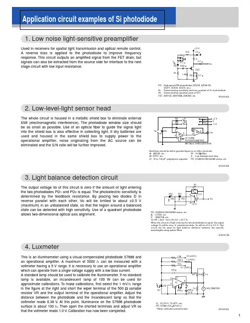
Application circuit examples of Si photodiode1. Low noise light-sensitive preamplifierUsed in receivers for spatial light transmission and optical remote control. A reverse bias is applied to the photodiode to improve frequency response. This circuit outputs an amplified signal from the FET drain, but signals can also be extracted from the source side for interface to the next stage circuit with low input resistance.KPDC0014ED2. Low-level-light sensor headThe whole circuit is housed in a metallic shield box to eliminate external EMI (electromagnetic interference). The photodiode window size should be as small as possible. Use of an optical fiber to guide the signal light into the shield box is also effective in collecting light. If dry batteries are used and housed in the same shield box to supply power to the operational amplifier, noise originating from the AC source can be eliminated and the S/N ratio will be further improved.KPDC0016ED3. Light balance detection circuitThe output voltage Vo of this circuit is zero if the amount of light entering the two photodiodes PD1 and PD2 is equal. The photoelectric sensitivity is determined by the feedback resistance. By placing two diodes D in reverse parallel with each other, Vo will be limited to about ±0.5 V (maximum) in an unbalanced state, so that the region around a balanced state can be detected with high sensitivity. Use of a quadrant photodiode allows two-dimensional optical axis alignment.KPDC0017EB4. LuxmeterThis is an illuminometer using a visual-compensated photodiode S7686 and an operational amplifier. A maximum of 5000 lx can be measured with a voltmeter having a 5 V range. It is necessary to use an operational amplifier which can operate from a single voltage supply with a low bias current.A standard lamp should be used to calibrate the illuminometer. If no standard lamp is available, an incandescent lamp of 100 W can be used for approximate calibrations. To make calibrations, first select the 1 mV/lx range in the figure at the right and short the wiper terminal of the 500 9 variable resistor VR and the output terminal of the operational amplifier. Adjust the distance between the photodiode and the incandescent lamp so that the voltmeter reads 0.38 V. At this point, illuminance on the S7686 photodiode surface is about 100 lx. Then open the shorted terminals and adjust VR so that the voltmeter reads 1.0 V. Calibration has now been completed.KPDC0018EC-+ISC2ISC1PD2PD1RfDD23764-15 V+15 VVoA10 k10 µ+15 V1 k0.1 µFET0.1 µRS1 MRLPD0.1 µ1000 p10 µVo++PD: High-speed PIN photodiodes (S5052, S2506-02,S5971, S5972, S5973, etc.)RL: Determined by sensitivity and time constant of Ct of photodiodeRS: Determined by operation point of FETFET: 2SK152, 2SK192A, 2SK362, etc. PDVo236A1-+326+5 V-5 V0CfRf2Rf1S1S210-TURNPOTENTIOMETER10 µ10 µ++A2-+51METALIC SHIELDED BOXISCBold lines should be within guarded layout or on teflon terminals.A1:AD549, etc.Rf : 10 G9 Max. A2 :OP07, etc.S : Low-leakage reed relayCf:10 to 100 pF, polystyrene capacitorPD: S1226/S1336/S2386 series, etc.PD: S1226/S1336/S2386 series, etc.A: LF356, etc.D: ISS270A, etc. Vo=Rf × (Isc2 - Isc1) (V) (Vo < ±0.5 V)When the amount of light entering the two photodiodes is equal, the output voltage Vo will be zero. In unbalanced state, Vo will be ±0.3 to 0.5 V. This circuit can be used for light balance detection between two specific wavelengths using optical filters.IC : ICL7611, TLC271, etc.PD: S7686 (3.8 µA/100 lx)* Meter calibration potentiometer100 p1 k1 kPD10 k100 k1 M200 p006 p(9 V)VOLTMETER500VR *76843210.1 (mV/lx)1 (mV/lx)10 (mV/lx)IC+-IscV15. Light sensor using high-speed operational amplifier (1)This circuit uses a high-speed photodiode applied at a reverse voltage and a current-to-voltage conversion operational amplifier. The time response of the circuit greatly depends on the time constant of the feedback resistance Rf and its parallel stray capacitance. To minimize the effect of this time constant, two or more resistors are connected in series as the feedback resistance to disperse the parallel stray capacitance. Use of chip resistors as the feedback resistance will be effective in reducing the stray capacitance.KPDC0020EE6. Light sensor using high-speed operational amplifier (2)This light detection circuit uses a high-speed, current-feedback operational amplifier, and allows direct connection to a coaxial cable. Because this circuit performs signal amplification after current-to-voltage conversion by load resistance RL, there will be no detrimental effects which result from a phase shift in the amplifier. As with the circuit 5., two or more resistors are used as the feedback resistance to disperse parallel stray capacitance in the resistors. A ceramic capacitor of 0.1 µF is connected to the power supply pin of the IC, and should be grounded at a minimum distance. For bandwidths over 100 MHz, use of chip resistors and capacitors is recommended to reduce the entire circuit size and suppress the undesired effects of lead inductance of each component. Performance can also be improved by using a ground plane structure in which the entire copper foil surface on the PCB is used at the ground potential.KPDC0015ED7. Light-to-logarithmic-voltage conversion circuitThe output voltage of this circuit is proportional to the logarithmic change in the detected light level. A base-emitter junction of small signal transistors or a diode between the gate-source of junction FETs can be used as the log diode D1. IB is the current source that supplies the log diode with a bias current. If IB is not present, the circuit will be unstable or latched up when Isc by the incident light decreases to zero.KPDC0021EA8. High-speed light detector using PIN photodiodeThis circuit uses no active components. Since no signal amplification is performed, this circuit is mainly used for detection at relatively high light levels. The impedance matching load resistance of 50 9 can be directly connected to the 50 9 input terminal of an oscilloscope or other measurement equipment.High-speed photodiodes designed for the GHz range can be used with this circuit. A chip capacitor should be used as the bypass capacitor C. The photodiode leads and the conductors of the coaxial cable where high-frequency current flows should be made as short as possible. Since the signal current flows instantaneously to the load from the capacitor C in the figure, it is necessary to select the capacitance that supplies the corresponding electric charge.In the figure at the right, if the cable is not terminated, the center conductor is charged up at the power supply potential. If a high reverse bias is used, sufficient caution must be taken not to exceed the maximum rating of the input circuit of the measurement equipment, otherwise the equipment may be damaged.

学习笔记
业精于勤! 红外发射二极管学习
一:红外发射管基本原理及应用
1、 发光二极管LED(Light Emitting Diode):
LED是由半导体材料所制成的光电元件,元件具有两个电极端子,在端子间施加电压,通入极小的电流便可发光;即:LED的发光原理是施加电压于AlGaAs(砷化铝镓)、AlGaInP(磷化铝铟镓)及GaInN(氮化铟镓)等化合物半导体上,
借着电子与空穴复合释放出过剩的能量而发光,发光现象不是藉加热发光,属于冷发光。LED利用3-5族化合物半导
体材料及元件结构之变化,进而设计产出各种颜色之固态电源,由于材料不同所释出来的波长也不同,包括红、橙、
蓝、绿、黄等可见光,以及红外光等不可见光的LED,种类繁多。
2、 红外发光二级管Infraed LED
由红外辐射效率高的材料(常用砷化镓GaAs)制成PN结,外加正向偏压向PN结注入电流激发红外光。光谱功
率分布为中心波长830~950nm,半峰带宽约40nm左右,它是窄带分布,为普通CCD黑白摄像机可感受的范围。其
最大的优点是可以完全无红暴,(采用940~950nm波长红外管)或仅有微弱红暴(红暴为有可见红光)和寿命长。
光是一种电磁波,它的波长区间从几个纳米(1nm=10-9m)到1毫米(mm)左右。人眼可见的只是其中一部分,
我们称其为可见光,可见光的波长范围为380nm~780nm,可见光波长由长到短分为红、橙、黄、绿、青、兰、紫光,
波长比紫光短的称为紫外光,波长比红外光长的称为红外光。
3、 红外发光二极管识别
红外发光二极管,外形与普通发光二极管、光电二极管和光电三极管相似,极易造成混淆,应当注意辨别。红外发光二极管大多采用无色透明树脂封装或黑色、淡蓝色树脂封装三种形式,无色透明树脂封装的管子,可以透过树脂
材料观察,若管芯下有一个浅盘,即是红外发光二极管,光电二极管和光电三极管无此浅盘; 4、红外发光二极管的极性