一些CPU设计实例
- 格式:ppt
- 大小:82.50 KB
- 文档页数:38

计算机组成原理实验题目8位CPU得系统设计学号1115106046姓名魏忠淋班级 11电子B 班指导老师凌朝东华侨大学电子工程系8位CPU得系统设计一、实验要求与任务完成从指令系统到CPU得设计,编写测试程序,通过运行测试程序对CPU设计进行正确性评定。
具体内容包括:典型指令系统(包括运算类、转移类、访存类)设计;CPU结构设计;规则文件与调试程序设计;CPU调试及测试程序运行。
1。
1设计指标能实现加减法、左右移位、逻辑运算、数据存取、有无条件跳转、内存访问等指令;1、2设计要求画出电路原理图、仿真波形图;二、CPU得组成结构三、元器件得选择1.运算部件(ALU)ALU181得程序代码:LIBRARY IEEE;USEIEEE、STD_LOGIC_1164。
ALL;USEIEEE、STD_LOGIC_UNSIGNED.ALL;ENTITY ALU181 ISPORT(S: IN STD_LOGIC_VECTOR(3 DOWNTO0 );A:IN STD_LOGIC_VECTOR(7 DOWNTO0);B: INSTD_LOGIC_VECTOR(7DOWNTO 0);F : OUT STD_LOGIC_VECTOR(7 DOWNTO 0);ﻩCOUT:OUTSTD_LOGIC_VECTOR(3 DOWNTO0);M :INSTD_LOGIC;CN : IN STD_LOGIC;CO,FZ:OUT STD_LOGIC );END ALU181;ARCHITECTURE behav OF ALU181 ISSIGNALA9 :STD_LOGIC_VECTOR(8DOWNTO 0);SIGNAL B9 : STD_LOGIC_VECTOR(8 DOWNTO0);SIGNALF9: STD_LOGIC_VECTOR(8 DOWNTO0);BEGINA9<= '0'& A; B9 <= ’0’&B;PROCESS(M,CN,A9,B9)BEGINCASE S ISWHEN "0000" =〉IF M='0’THEN F9<=A9 + CN ; ELSE F9<=NOT A9; E NDIF;WHEN "0001" =>IF M='0’THEN F9<=(A9 orB9)+ CN ;ELSE F9〈=NOT(A9OR B9);END IF;WHEN ”0010"=> IF M=’0’THEN F9〈=(A9 or(NOT B9))+C N; ELSE F9<=(NOT A9) ANDB9; ENDIF;WHEN "0011"=> IF M='0’THEN F9<= ”000000000"—CN ;ELSEF9<="000000000”;END IF;WHEN"0100”=> IFM='0'THENF9<=A9+(A9 ANDNOT B9)+ CN; ELSE F9〈=NOT(A9 ANDB9);END IF;WHEN ”0101”=>IFM='0' THENF9<=(A9orB9)+(A9 AND NOTB9)+CN ;ELSEF9<=NOT B9; END IF;WHEN"0110" =>IFM=’0’THEN F9〈=(A9- B9) -CN ;ELSE F9〈=A9XOR B9; ENDIF;WHEN”0111"=>IF M='0' THEN F9〈=(A9 or(NOT B9)) -CN ;ELSE F9<=A9 and (NOT B9); END IF;WHEN"1000" =>IFM='0'THEN F9<=A9+ (A9AND B9)+CN ; ELSE F9〈=(NOTA9)and B9; END IF;WHEN "1001”=> IF M=’0’THEN F9〈=A9+ B9 + CN ; ELSE F9<=NOT(A9 XOR B9); ENDIF;WHEN ”1010"=>IF M=’0'THEN F9〈=(A9or(NOTB9))+(A 9AND B9)+CN ; ELSEF9<=B9;END IF;WHEN "1011”=〉IF M='0'THENF9<=(A9 AND B9)- C N; ELSE F9<=A9 ANDB9; ENDIF;WHEN ”1100”=〉IF M='0'THENF9<=(A9 +A9) + CN; ELSEF9〈="000000001"; END IF;WHEN "1101”=〉IF M='0' THEN F9〈=(A9or B9)+ A9 + CN;ELSEF9〈=A9 OR (NOTB9); END IF;WHEN "1110"=>IF M='0'THENF9<=((A9 or (NOTB9)) +A9) + CN; ELSE F9〈=A9OR B9;END IF;WHEN”1111”=〉IFM=’0'THENF9<=A9 —CN ;ELSE F9<=A9 ; END IF;WHEN OTHERS=> F9<= ”000000000" ;ENDCASE;IF(A9=B9) THENFZ<=’0';END IF;ﻩEND PROCESS;F<=F9(7DOWNTO0) ;CO<= F9(8) ;COUT<="0000"WHEN F9(8)=’0'ELSE"0001";END behav;ALU得原理图:2、微控制器实现信息传送要靠微命令得控制,因此在CPU 中设置微命令产生部件,根据控制信息产生微命令序列,对指令功能所要求得数据传送进行控制,同时在数据传送至运算部件时控制完成运算处理。
第4章简单MIPS CPU设计4.1引言在本章中,我们为MIPS指令集的两种不同实现方式建立数据通路和控制单元。
我们将要设计的实现方式包含了MIPS指令集的一个核心子集:存储器访问指令:取字(1w)和存储字(sw)。
算术逻辑指令:加法(add),减法(sub),与运算(and),或运算(0r)和小于则设置(slt)。
分支指令:相等则转移(beq)和跳转(j)。
这个子集没有包括所有的整数指令(如缺乏乘除指令),也不包括任何浮点数指令。
但是,在建立数据通道和设计控制部分时用到的关键原理都会得以体现。
其余指令的实现也是类似的。
在学习此实现方式时,我们将有机会看到指令集如何影响实现方式的多个方面。
在本章及下一章中用于实现MIPS子集的大多数概念与很多计算机的基本构造思想是一致的。
4.1.1 实现方式概述在前一章节中,我们学习了MIPS的核心指令,包括整数算术逻辑指令、存储访指令及分支指令。
这些指令的实现过程大致相同,而与具体的指令类型无关。
实现每条指令的前两步是一样的:1)程序计数器(PC)指向指令所在的存储单元,并从中取出指令。
2)通过指令字段内容,选择读取一或两个寄存器。
对于取字指令,只需读取一个寄存器,而其他大多数指令要求读取两个。
这两步之后,为完成指令而进行的步骤则取决于具体的指令类型。
幸运的是,对三种指令类型(存储访问、算术逻辑、分支)的每一种而言,其动作大致相同,与具体操作码无关。
即使是不同类型的指令,也有一定的共性。
例如,所有类型的指令在读取寄存器后,都要使用算术逻辑单元(ALU)。
存储访问指令用ALU计算地址,算术逻辑指令用来执行运算,分支指令用ALU进行比较。
可以看出,指令的简洁和规整使许多指令的执行很相似,因而简化了实现过程。
使用ALU之后,不同类型指令需要进行不同的操作。
存储访问指令需要对存储单元进行读出或写入;算术逻辑指令需要将ALU产生的数据写回寄存器中;而分支指令会根据比较的结果,决定是否需要更改下条指令的地址。


计算机组成原理CPU设计实验报告课程设计题目:16位CPU设计学院: 信息学院班级:电子A班学号:1115102015姓名:方茹1目录1 实验方法 ..................................................................... . (4)2 总体说明 ..................................................................... ................................................. 5 2.1指令系统: .................................................................... .......................... 5 2.1.1指令格式分类(按指令字长和操作数不同): ...................................................... 5 2.1.2具体指令汇总表: .................................................................... .......................... 6 2.1.3相关指令流程图: .................................................................... .......................... 6 2.1.4指令数据通路的构建: .................................................................... ................... 8 2.1.5指令的分组及节拍: .................................................................... ..................... 12 2.1.6指令执行状态图:(见下页)..................................................................... ........... 13 2.1.7具体微指令: .................................................................... ............................... 13 2.2 系统整体介绍 ..................................................................... .................. 16 2.2.1系统基本模块划分 ..................................................................... ....................... 16 2.2.2总体结构图:(见下页)..................................................................... (17)3 CPU的控制逻辑与具体数据通道设计 ..................................................................... ......18 3.1取指令逻辑的设计 ..................................................................... .. (19)3.1.1指令地址的保存 ..................................................................... (19)3.1.2指令存储器 ..................................................................... .................................. 20 3.1.3下一条指令地址的计算 ..................................................................... ................ 20 3.2指令译码逻辑的设计...................................................................... ...................... 21 3.3指令执行逻辑的设计...................................................................... ...................... 22 3.4存储器访问逻辑的设计 ..................................................................... ................... 23 3.5结果写回逻辑的设计...................................................................... ...................... 24 3.6单周期CPU的总成...................................................................... (25)4各部分说明 ..................................................................... .............................................26 4.1ALU .................................................................................................................... 26 4.2数据选择器BUS_MUX ................................................................ ........................ 28 4.3器件T1 ..................................................................... .......................................... 30 4.4标志寄存器FLAG_REG ............................................................... ........................ 31 4.5T2: .................................................................... ................................................ 33 4.6程序计数器PC ..................................................................... ............................... 33 4.7地址寄存器AR和指令寄存器IR: .................................................................... .. 34 4.8寄存器、寄存器组和寄存器的选择.......................................................................36 4.9一位控制信号/WR .................................................................... ........................... 37 4.10 节拍发生器 ..................................................................... .................................. 37 4.11控制逻辑 ..................................................................... ...................................... 39 4.12T3...................................................................... ................................................ 42 4.13REG_OUT ......................................................................................................... 43 4.14存储器 ..................................................................... .......................................... 44 4.15总线选择器 ..................................................................... .. (45)24.16REG_TEST ............................................................... .. (46)5附录: .................................................................... .. (47)附录A:组员分工: .................................................................... .. (47)附录B:组员设计总结: .................................................................... . (47)31 实验方法实验要完成的工作主要包括:指令系统的设计,FPGA-CPU的整体结构设计及其细化,逻辑设计的具体实现(VHDL语言程序的编写),软件模拟,以及硬件调试。
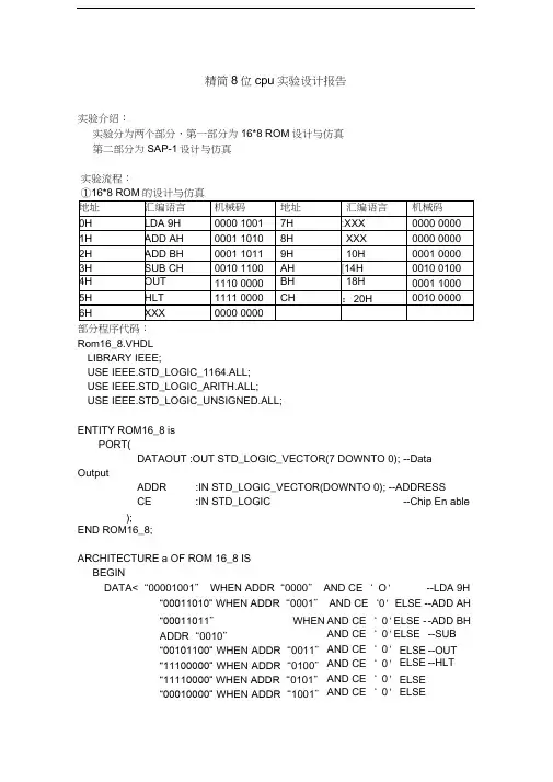
“00011011” WHEN ADDR “0010”“00101100” WHEN ADDR “0011”“11100000” WHEN ADDR “0100”“11110000” WHEN ADDR “0101” “00010000” WHEN ADDR “1001”AND CE ‘ 0'E LSE - -ADD BH AND CE ‘ 0' E LSE --SUB CH AND CE ‘ 0' ELSE --OUT AND CE ‘ 0' ELSE --HLT AND CE ‘ 0' ELSEAND CE ‘ 0' ELSE精简8位cpu 实验设计报告实验介绍:实验分为两个部分,第一部分为16*8 ROM 设计与仿真 第二部分为SAP-1设计与仿真 实验流程:①16*8 ROM 的设计与仿真部分程序代码:Rom16_8.VHDL LIBRARY IEEE;USE IEEE.STD_LOGIC_1164.ALL; USE IEEE.STD_LOGIC_ARITH.ALL;USE IEEE.STD_LOGIC_UNSIGNED.ALL;ENTITY ROM16_8 isPORT(DATAOUT :OUT STD_LOGIC_VECTOR(7 DOWNTO 0); --DataOutputADDR :IN STD_LOGIC_VECTOR(DOWNTO 0); --ADDRESS CE :IN STD_LOGIC --Chip En able );END ROM16_8;ARCHITECTURE a OF ROM 16_8 IS BEGINDATA<“00001001” WHEN ADDR “0000” AND CE ‘ O '“00011010” WHEN ADDR “0001” AND CE ‘0' ELSE --ADD AH--LDA 9H“00011000”WHEN ADDR=“1011”AND CE=‘0'ELSE“00100000”WHEN ADDR=“1100”AND CE=‘0'ELSE“00000000”;END a;程序说明:rom的使能CE只有为0时,才接受读数据的命令。
16位实验CPU设计实例开放式CPU指的是CPU在一片FPGA芯片中构成,它的指令系统和CPU内部结构可以由使用者根据需要设计,并且能够在TEC-CA上进行调试的CPU。
实验CPU是学生为掌握计算机的工作原理而设计的CPU,主要针对基本原理而不强调完备性。
这样的CPU可以复杂一些,也可以简单一些,视学生水平而定。
本章中介绍的实验CPU实例是针对第6章计算机组成原理实验而设计的,使用者可在此基础上根据自己的需要进行适当增减。
计算机组成原理实验除了进行计算机各部件的实验外,最重要的是使学生掌握计算机整机的工作原理。
我们力求通过这个实验CPU设计实例,使学生能够深入掌握计算机的整机工作原理。
2.1 指令系统设计CPU首先要设计指令系统。
由于实验CPU采用16位字长,指令系统只有15条指令,因此比8位CPU的指令系统设计容易得多。
2.1.1 指令系统ADD DR,SR指令编码:0000 DR SR 0000 0111功能:DR ← DR + SR, 影响C和Z标志。
PC ← PC + 1。
INC DR指令编码:0001 DR SR 0000 0111功能:DR ← DR + 1,影响C和Z标志。
PC ← PC + 1。
SUB DR,SR指令编码:0010 DR SR 0000 0111功能:DR ← DR – SR,影响C和Z标志。
PC ← PC + 1。
DEC DR指令编码:0011 DR SR 0000 0111功能:DR ← DR – 1,影响C和Z标志。
PC ← PC + 1。
AND DR,SR指令编码:0100 DR SR 0000 0011功能:DR ← DR and SR,影响Z标志。
PC ← PC + 1。
OR DR,SR指令编码:0101 DR SR 0000 0011功能:DR ← DR or SR,影响Z标志。
PC ← PC + 1。
NOT DR指令编码:0110 DR SR 0000 0011功能:DR ← not DR,影响Z标志。
作业:10、解:对非常简单CPU增加了一条CLEAR指令后的新的状态图如下:其RTL代码如下:FETCH1:AR PCFETCH2:DR M, PC PC+1FETCH3:IR DR[7..6], AR DR[5,0]ADD1:DR MADD2:AC AC+DRAND1:DR MAND2:AC AC^DRJMP :PC DR[5..0]R5 :DR[5] 1 或DR[5] 0INC :AC AC+1CLEAR:AC 011、解:一、确定CPU的用途以下设计的CPU是要用来执行取反运算、加法运算、逻辑或运算、减法运算这四条指令的,而且该CPU能够访问64个字的存储器,每个字为8位宽。
字长:8位D[7....0]寻址范围:64Btye ,2^6=64,A[5....0]二、确定ISA1、程序员可访问的寄存器在下表中,为了完成COM , JREL , OR 和SUB1这四条指令,显然我们只需用到一个通用寄存器AC——8位累加器就可以实现。
指令操作码操作COM 00XX XXXX AC AC' (取反)JRET 01AA AAAA PC PC+00AA AAAAOR 10AA AAAA AC AC^M[00AA AAAA]SUB1 11AA AAAA AC AC—M[00AA AAAA]—12、CPU还需要一些其他的寄存器以便完成取指令(或数据)、译码和执行指令所必须的内部操作,最基本的寄存器有:AR(地址寄存器)——6位,由A[5.....0]向存贮提供地址PC (程序计数器)——6位,指出下一条指令的地址DR(数据寄存器)——8位,通过D[7....0]从存贮器接受指令和数据IR(指令寄存器)——2位,存放从存贮器中取回的指令的操作码部分。
三、为CPU设计状态图为了确定CPU的状态图,需对每条指令作如下分析:1、从存贮器取出指令(所有指令都相同)2、指令译码3、指令执行从存贮器中取出指令:1、原理:根据冯. 诺依曼型机的原理(指令在存贮器中按顺序存放.......), 在CPU能执行指令之前,它必须将这条指令从存贮中取出,CPU通过执行如下的操作序列完成这个任务的:【1】选择存贮单元由A[5... 0]确定【2】对A[5... 0]译码、延迟、并向存贮器发一个信号(如READ或R/W'=1),使存贮器将此指令输出到它的输出引脚。
LatticeMico8 Processor Reference ManualDecember 2012CopyrightCopyright © 2012 Lattice Semiconductor Corporation.This document may not, in whole or part, be copied, photocopied, reproduced, translated, or reduced to any electronic medium or machine-readable form without prior written consent from Lattice Semiconductor Corporation.TrademarksLattice Semiconductor Corporation, L Lattice Semiconductor Corporation (logo), L (stylized), L (design), Lattice (design), LSC, CleanClock, Custom Movile Device, DiePlus, E2CMOS, Extreme Performance, FlashBAK, FlexiClock, flexiFLASH, flexiMAC, flexiPCS, FreedomChip, GAL, GDX, Generic Array Logic, HDL Explorer, iCE Dice, iCE40, iCE65, iCEblink, iCEcable, iCEchip, iCEcube, iCEcube2, iCEman, iCEprog, iCEsab, iCEsocket, IPexpress, ISP, ispATE, ispClock, ispDOWNLOAD, ispGAL, ispGDS, ispGDX, ispGDX2, ispGDXV, ispGENERATOR, ispJTAG, ispLEVER, ispLeverCORE, ispLSI, ispMACH, ispPAC, ispTRACY, ispTURBO, ispVIRTUAL MACHINE, ispVM, ispXP, ispXPGA, ispXPLD, Lattice Diamond, LatticeCORE, LatticeEC, LatticeECP, LatticeECP-DSP, LatticeECP2, LatticeECP2M, LatticeECP3, LatticeECP4, LatticeMico, LatticeMico8, LatticeMico32, LatticeSC, LatticeSCM, LatticeXP, LatticeXP2, MACH, MachXO, MachXO2, MACO, mobileFPGA, ORCA, PAC, PAC-Designer, PAL, Performance Analyst, Platform Manager, ProcessorPM, PURESPEED, Reveal, SiliconBlue, Silicon Forest, Speedlocked, Speed Locking, SuperBIG, SuperCOOL, SuperFAST, SuperWIDE, sysCLOCK, sysCONFIG, sysDSP, sysHSI, sysI/O, sysMEM, The Simple Machine for Complex Design, TraceID, TransFR, UltraMOS, and specific product designations are either registered trademarks or trademarks of Lattice Semiconductor Corporation or its subsidiaries in the United States and/or other countries. ISP, Bringing the Best Together, and More of the Best are service marks of Lattice Semiconductor Corporation.Other product names used in this publication are for identification purposes only and may be trademarks of their respective companies.DisclaimersNO WARRANTIES: THE INFORMATION PROVIDED IN THIS DOCUMENT IS “AS IS” WITHOUT ANY EXPRESS OR IMPLIED WARRANTY OF ANY KIND INCLUDING WARRANTIES OF ACCURACY, COMPLETENESS, MERCHANTABILITY, NONINFRINGEMENT OF INTELLECTUAL PROPERTY, OR FITNESS FOR ANY PARTICULAR PURPOSE. IN NO EVENT WILL LATTICE SEMICONDUCTOR CORPORATION (LSC) OR ITS SUPPLIERS BE LIABLE FOR ANY DAMAGES WHATSOEVER (WHETHER DIRECT, INDIRECT, SPECIAL, INCIDENTAL, OR CONSEQUENTIAL, INCLUDING, WITHOUT LIMITATION, DAMAGES FOR LOSS OF PROFITS, BUSINESS INTERRUPTION, OR LOSS OF INFORMATION) ARISING OUT OF THE USE OF OR INABILITY TO USE THE INFORMATION PROVIDED IN THIS DOCUMENT, EVEN IF LSC HAS BEEN ADVISED OF THE POSSIBILITY OF SUCH DAMAGES. BECAUSE SOME JURISDICTIONS PROHIBIT THE EXCLUSION OR LIMITATION OF CERTAIN LIABILITY, SOME OF THE ABOVE LIMITATIONS MAY NOT APPLY TO YOU.LSC may make changes to these materials, specifications, or information, or to the products described herein, at any time without notice. LSC makes no commitment to update this documentation. LSC reserves the right to discontinue any product or service without notice and assumes no obligation to correct any errors contained herein or to advise any user of this document of any correction if such be made. LSC recommends its customers obtain the latest version of the relevant information to establish, before ordering, that the information being relied upon is current.Type Conventions Used in This DocumentConvention Meaning or UseBold Items in the user interface that you select or click. Text that you type into the user interface.<Italic>Variables in commands, code syntax, and path names.Ctrl+L Press the two keys at the same time.Courier Code examples. Messages, reports, and prompts from the software. ...Omitted material in a line of code.Omitted lines in code and report examples....[ ]Optional items in syntax descriptions. In bus specifications, the brackets are required.( )Grouped items in syntax descriptions.{ }Repeatable items in syntax descriptions.| A choice between items in syntax descriptions.ContentsIntroduction 1Architecture 3Register Architecture3General-Purpose Registers3Control and Status Registers4 Memory Architecture5Memory Regions5Memory Modes9Interrupt Architecture10Call Stack10Configuration Options 11Instruction Set 13Instruction Formats13Instruction Set Lookup Table14 Instruction Descriptions16Programming Model 37Data Representation37Procedure Caller-Callee Convention38 Register Usage38Stack Frame39Parameter Passing40Interrupt Convention41Acessing LatticeMico8 Memory Regions42 Scratchpad42Peripheral42PROM43C ONTENTSIndex 45Chapter 1 IntroductionThe LatticeMico8™ is an 8-bit microcontroller optimized for Field Programmable Gate Arrays (FPGAs) and Programmable Logic Device architectures from Lattice Semiconductor. It combines a full 18-bit wide instruction set with 16 or 32 general-purpose registers. It is suitable for a wide variety of markets, including communications, consumer, computer, medical, industrial and automotive. The core consumes minimal device resources— fewer than 250 Look-Up Tables (LUTs) in the smallest configuration—while maintaining a broad feature set.LatticeMico8 Features◆8-Bit Data Path◆18-Bit Instructions◆Configurable Instruction Memory (PROM)◆Internal, or external through the WISHBONE Interface◆Configurable to accommodate 256, 512, 1K, 1.5K, 2K, 2.5K, 3K, 3.5Kor 4K instructions◆Scratchpad Memory◆Internal, or external through the WISHBONE Interface◆Configurable up to 4Gbytes using paged bytes (256 bytes/page)◆Input/Output Peripheral Space through the WISHBONE Interface◆Configurable up to 4Gbytes using paged ports (256 ports/page)◆Minimum Two Cycles per Instruction◆Configurable 16 or 32 General-purpose Registers◆Configurable Call Stack sizeFigure1 on page2 shows the LatticeMico8 Microcontroller block diagram.I NTRODUCTION:Figure 1: LatticeMico8 Microcontroller CoreChapter 2ArchitectureThis chapter describes the LatticeMico8 register and memory architectureand explains the interrupt architecture and call stack.Register ArchitectureThis section describes the general-purpose and control and status registers ofthe LatticeMico8 architecture.General-Purpose RegistersThe LatticeMico8 microcontroller can be configured to have either 16 or 32general-purpose registers. Each register is 8 bits wide. The registers areimplemented using a dual-port distributed memory. The LatticeMico8 opcodeset permits the microcontroller to access 32 registers. When LatticeMico8 isconfigured with 16 registers, any opcode reference to R16 to R31 maps to R0to R15 respectively.General-purpose registers R13, R14, and R15 can also be used by theLatticeMico8 microcontroller as page-pointer registers, depending on thecurrent memory mode. Page pointers (PP) are used when the scratchpad andperipheral memory spaces are larger than 256 bytes (see “Memory Modes”on page9). The memory address is formed by concatenating the values inregisters R13, R14, and R15 with an 8-bit value derived from the LatticeMico8memory instruction. Table1 on page4 highlights the three LatticeMico8memory modes and corresponding designation of registers R13, R14, andR15.In the large memory mode, registers R13, R14, and R15 indicate which ofthe 16M pages is currently active. R13 provides the least-significant byteof page address and R15 provides most-significant byte.A RCHITECTURE :Register ArchitectureIn the medium memory mode, register R13 indicates which of the 256pages is currently active.Control and Status RegistersTable 2 shows all the names of the control and status registers (CSR), theread and write access, and the index used when the register is accessed. Allsignal levels are active high.IP – Interrupt Pending The IP CSR contains a pending bit for each of the 8external interrupts. A pending bit is set when the corresponding interruptrequest line is asserted low. Bit 0 corresponds to interrupt 0. Bits in the IPCSR can be cleared by writing a 1 with the wcsr instruction. Writing a 0 has noeffect. After reset, the value of the IP CSR is 0.IM – Interrupt Mask The IM CSR contains an enable bit for each of the 8external interrupts. Bit 0 corresponds to interrupt 0. In order for an interrupt tobe raised, both an enable bit in this register and the IE flag in the IE CSR mustbe set to 1. After reset, the value of the IM CSR is 0.IE – Global Interrupt Enable The IE CSR contains a single-bit (bit position0) flag, IE, which determines whether interrupts are enabled. This flag haspriority over the IM CSR. After reset, the value of the IE CSR is 0.Table 1: Designation of LatticeMico8 Registers Based on LatticeMico8 Memory ModeRegister NumberLatticeMico8 Memory ModeSmall Medium Large 0 through 12general-purpose general-purpose general-purpose 13general-purpose PP PP (LSB)14general-purpose general-purpose PP 15general-purpose general-purpose PP (MSB)16 through 31general-purpose general-purpose general-purposeTable 2: Control and Status RegistersNameAccess Index Description IPR/W 0Interrupt Pending IMR/W 1Interrupt Mask IE R/W 2Global Interrupt Enable/DisableA RCHITECTURE:Memory ArchitectureMemory ArchitectureThis section describes the memory architecture of the LatticeMico8microcontroller.Memory RegionsThe LatticeMico8 microcontroller recognizes three independent memoryregions. Each memory region has its own independent input/output interfaceand its own instruction set support. These three memory regions are calledthe PROM, the Scratchpad, and the Peripheral memory regions respectively.The size and location of each of these memory regions is configurable as longas all these three memory regions are located entirely within the 4GB addressspace. These memory regions can also be configured to overlap withinLatticeMico System Builder. Figure2 shows the three memory regions andthe address space to which they are confined by LatticeMico System Builder.See “Acessing LatticeMico8 Memory Regions” on page42 for details on howto access each of the three memory regions from a software programmer'sperspective.Figure 2: Memory OrganizationA RCHITECTURE:Memory ArchitecturePROM SpaceThe PROM memory region contains the program code that will be executedby the LatticeMico8 microcontroller core and is accessible via its instructionfetch engine. The size of the PROM memory region can be configured toaccommodate 256, 512, 1024, 2048, or 4096 instruction opcodes. By defaultthe memory region is located within the LatticeMico8 microcontroller. Thememory regions can also be configured to be external to the LatticeMico8microcontroller.When the PROM memory region is internal to the microcontroller, it isconnected to the LatticeMico8 instruction fetch engine via a dedicated high-speed bus that fetches one instruction opcode per clock cycle. There is noinstruction set support to write to internal PROM. When the PROM memoryregion is external to the microcontroller, it is accessed by the masterWISHBONE interface within the LatticeMico8 instruction fetch engine. ThisWISHBONE interface has a 8-bit data bus and it takes three 8-bit WISHBONEaccesses to fetch one LatticeMico8 instruction opcode. The instruction fetchlatency is now dictated by the system WISHBONE latency and the latency ofthe PROM memory. The minimum instruction fetch latency is 12 clock cycles.Table3 shows the WISHBONE interface signals. For more information aboutthe WISHBONE System-On-Chip (SoC) Interconnection Architecture forPortable IP Cores, as it is formally known, refer to the Web site at /projects.cgi/web/wishbone.Table 3: PROM WISHBONE Interface SignalsName Width Direction DescriptionI_CYC_O1Output A new LatticeMico8 instruction fetch request is initiated by asserting thissignal. This signal remains asserted until I_ACK_I is asserted, whichindicates the completion of the request.I_STB_O1Output A new LatticeMico8 instruction fetch request is initiated by asserting thissignal. This signal may be valid only for the first cycle.I_CTI_O2Output Always has a value 2’b00I_BTE_O3Output Always has a value 3’b000I_ADR_O32Output The address output array I_ADR_O( ) is used to pass a binary address.I_WE_O1Output Always has a value 1’b0I_SEL_O4Output Always has a value 4’b1111I_DAT_O8Output UnusedI_LOCK_O1Output Unused (signal exists, but it is not implemented)I_ACK_I1Input When asserted, the signal indicates the normal termination of a bus cycleand that an instruction is available on I_DAT_I bus.I_ERR_I1Input Unused (signal exists, but it is not implemented)I_RTY_I1Input Unused (signal exists, but it is not implemented)I_DAT_I8Input One byte of the LatticeMico8 18-bit instruction opcode is available on thisbus when I_ACK_I is asserted. It takes three WISHBONE transactions tocomplete one LatticeMico8 instruction fetch.A RCHITECTURE :Memory ArchitectureThe advantage of configuring the PROM memory region as external to the LatticeMico8 microcontroller is that the PROM memory region can now be configured to overlap with other LatticeMico8 memory regions within Lattice Mico System Builder and, therefore, be directly written to by LatticeMico8 opcodes. This configuration also offers the ability to store and executeLatticeMico8 instructions from non-volatile memory such as Flash. As shown in Figure 2 on page 5, the external PROM memory region can be placed at any location within a 4GB address range. When the LatticeMico8microcontroller is instantiated using Lattice Mico System Builder, it will restrict the placement of external PROM between 0x00000000 and 0x80000000.Scratchpad SpaceLatticeMico8 provides an independent memory space that is designed to be used for program read/write and read-only data as well as other user-defined data. The size of this scratchpad memory can be configured from 32 bytes to 4G bytes, in power-of-two increments. Figure 3 shows the structure of this scratchpad space and how data is located within this space. The scratchpad memory space can be placed at any location within a 4GB address range. The first 4 bytes are reserved for LatticeMico8 interrupt handling. Program data is situated above this reserved space. The designer can configure the size of scratchpad memory that is used for program data. User-defined data is optional and is always located after program data.The scratchpad memory can be configured to be entirely internal to theLatticeMico8 microcontroller, entirely external to LatticeMico8 microcontroller, or a combination of both.◆The internal scratchpad is implemented using single-port EBRs and is hooked up to the LatticeMico8 core through a dedicated bus. Reads or writes to the internal scratchpad take a single clock cycle.◆The external scratchpad is accessed through the Peripheral WISHONE interface of the LatticeMico8 microcontroller (see “Interrupt Architecture” on page 10). Each read or write will take a minimum of 2 clock cycles.Figure 3: Scratchpad Space StructureA RCHITECTURE:Memory ArchitecturePeripheral (Input/Output) SpaceLatticeMico8 provides an independent memory space that is designed to beused for peripherals and other memory-mapped hardware. The size of thisperipheral memory space can be configured from 0 bytes to 4G bytes inpower-of-two increments. While the peripheral memory space can be placedat any location within a 4GB address range, Lattice Mico System Builderrestricts the peripheral memory space to the addresses between 0x80000000and 0xFFFFFFFF.This memory space is always external to the LatticeMico8 microcontroller andis primarily used to enable LatticeMico8 to communicate with memory-mapped hardware and peripherals. The LatticeMico8 microcontroller cancommunicate with any hardware or peripheral within the peripheral memoryspace, through the peripheral WISHBONE interface within LatticeMico8 core,using LatticeMico8 instruction opcodes. This WISHBONE interface has 8-bitinput and output data busses and a 32-bit address bus. Table4 shows thePeripheral WISHBONE interface signals.Table 4: Peripheral WISHBONE Interface SignalsName Width Direction DescriptionD_CYC_O1Output A new LatticeMico8 data request is initiated by asserting this signal.This signal remains asserted until D_ACK_I is asserted, whichindicates completion of the request.D_STB_O1Output A new LatticeMico8 data request is initiated by asserting this signal.This signal may be valid only for first cycle.D_CTI_O2Output This bus will always have a value 2'b00D_BTE_O3Output This bus will always have a value 3'b000D_ADR_O32Output The address output array D_ADR_O( ) is used to pass a binaryaddress. D_ADR_O( ) actually has a full 32 bits.D_WE_O1Output This signal indicates whether a new data request is a read (0) or awrite (1). This signal must hold its value as long as D_CYC_O isasserted.D_SEL_O1Output Always has a value 1'b1D_DAT_O8Output Has valid data when D_WE_O is 1'b1.D_LOCK_O1Output Unused (signal exists, but it is not implemented)D_ACK_I1Input When asserted, the signal indicates the normal termination of a buscycle.D_ERR_I1Input Unused (signal exists, but it is not implemented)D_RTY_I1Input Unused (signal exists, but it is not implemented)D_DAT_I8Input Data is available on this bus when D_ACK_I and D_WEO areasserted.A RCHITECTURE:Memory ArchitectureMemory ModesThe LatticeMico8 microcontroller can be configured for different sizes for thescratchpad and peripheral memory regions. The size of scratchpad andperipheral memory regions can be as small as 32 bytes and as large as 4Gbytes. A 32-byte memory region requires only 5 address bits, while a 4GBmemory region requires 32 address bits.The LatticeMico8 instruction set can directly access only 256 memorylocations, since all general-purpose registers are 8 bits wide. (See “InstructionSet” on page13.) To access memory regions that are larger than 256 bytes,LatticeMico8 relies on a concept called “paging,” in which the memory islogically divided into 256-byte pages. The memory address is composed oftwo parts, as shown in Figure4: the page index and the page pointer. Thepage index is 8 bits wide and addresses a byte in the currently active page,while the page pointer provides the address of the currently active page. Figure 4: Memory ModesThe page pointers are essentially general-purpose registers that have beenretargeted to provide a memory address. (See “Memory Regions” on page5.)Table5 shows the memory modes of the LatticeMico8 microcontroller, thesize of addressable memory space in each mode, and the general-purposeregisters used as page pointers.Table 5: LatticeMico8 Memory ModesMemory Mode Maximum Memory Size Address Bits Page Pointer RegistersSmall256 bytes8N/AMedium16K bytes16R13Large4G bytes32R13, R14, R15A RCHITECTURE:Interrupt ArchitectureInterrupt ArchitectureThe LatticeMico8 microcontroller supports up to 8 maskable, active-low, level-sensitive interrupts. Each interrupt line has a corresponding mask bit in the IMCSR. The mask enable is active high. A global interrupt-enable flag isimplemented in the IE CSR. The software can query the status of theinterrupts and acknowledge them through the IP CSR. If more interruptsources or more sophisticated interrupt detection methods are required,external interrupt controllers can be cascaded onto the microcontroller’sinterrupt pins to provide the needed functionality.When an interrupt is received, the address of the next instruction is pushedinto the call stack (see “Call Stack” on page10), and the microcontrollercontinues execution from the interrupt vector (address 0). The flags (carry andzero) are pushed onto the call stack along with the return address. An iretinstruction will pop the call stack and transfer control to the address on top ofthe stack. The flags (carry and zero) are also popped from the call stack.See “Interrupt Convention” on page41 for details on the programming modelfor interrupts.NoteThe LatticeMico8 microcontroller does not support nested interrupts. Locations 0through 3 in the scratchpad are reserved for interrupt handling and should not used forany other purpose.Call StackThe LatticeMico8 microcontroller implements a hardware call stack to handleprocedure calls (call instruction) and procedure/interrupt return (ret and iretinstructions). The depth of this call stack determines the number of nestedprocedure calls that can be handled by the LatticeMico8 microcontroller, anddesigners can choose the depth to be 8, 16, or 32. When a call instruction isexecuted, the address of the next instruction is pushed on to the call stack. Aret or iret instruction will pop the stack and continue execution from thelocation at the top of the stack.NoteThere is no mechanism in hardware to detect whether the number of nested procedurecalls has exceeded the depth of the call stack. It is up to the software developer toensure that the call stack does not overflow.Chapter 3Configuration OptionsThe LatticeMico8 microcontroller is reconfigurable. Table6 outlines thevarious configuration options that are available to a designer.Table 6: LatticeMico8 Configuration OptionsParameter Name DescriptionLATTICE_FAMILY The target Lattice FPGA family.CFG_PROM_INIT_FILE Provides the file that contains the initialization data (program code) for aninternal PROM.CFG_PROM_INIT_FILE_FORMAT Indicates whether CFG_PROM_INIT_FILE is in hex (default) or binary. CFG_PROM_SIZE Indicates the number of instructions that can be accommodated in thePROM.CFG_SP_INIT_FILE Provides the file that contains the initialization data (program data) for aninternal scratchpad.CFG_SP_INIT_FILE_FORMAT Indicates whether CFG_SP_INIT_FILE_FORMAT is hex (default) or binary. SP_PORT_ENABLE Indicates whether the scratchpad is internal (value 1) or external (value 0).The default is 1.SP_SIZE Indicates the number of bytes in the scratchpad.SP_BASE_ADDRESS Provides the base address of the scratchpad, regardless of whether it isinternal or external.CFG_IO_BASE_ADDRESS Provides the base address of the peripheral memory region.CFG_EXT_SIZE_[8|16|32]Indicates the size of address bus for the scratchpad and peripheral memoryregions and, therefore, identifies the LatticeMico8 memory mode. Thedefault is 16 (medium memory mode).CFG_REGISTER_[16|32]Indicates the number of general-purpose registers in LatticeMico8. Thedefault is 8.C ONFIGURATION O PTIONS:Table 6: LatticeMico8 Configuration Options (Continued)Parameter Name DescriptionCFG_CALL_STACK_[8|16|32]Indicates the depth of the call stack. The default is 16.CFG_ROM_EN Indicates whether the PROM and Scratchpad memories need to beinitialized from non-volatile storage such as flash at power-up. The defaultis 0, i.e., no copying is required.CFG_ROM_BASE_ADDRESS Provides the base address of the memory which contains the PROM andScratchpad images. The PROM image starts at this base address. TheScratchpad image starts at location (CFG_PROM_SIZE*3).CFG_XIP Indicates whether the PROM memory is the same as the non-volatilestorage that contains the PROM image. The default is 0, i.e., bothmemories are different. 1 indicates that both memories are the same (i.e.,no copying needs to be done) and the PROM is external to LatticeMico8. INTERRUPTS Indicates the number of external interrupts. The default is 8.Chapter 4Instruction SetThis chapter includes descriptions of all the instruction opcodes of theLatticeMico8 microcontroller.Instruction FormatsAll LatticeMico8 instructions are 18 bits wide. They are in three basic formats,as shown in Figure5, Figure6, and Figure7.Figure 5: Register-Register FormatFigure 6: Register-Immediate FormatFigure 7: Immediate FormatI NSTRUCTION S ET:Instruction Set Lookup TableInstruction Set Lookup TableTable 7: Instruction Set Reference CardOperation Action Flags ADD Rd, Rb Rd = Rd + Rb Carry, Zero ADDC Rd, Rb Rd = Rd + Rb + Carry Carry, Zero ADDI Rd, C Rd = Rd + C Carry, Zero ADDIC Rd, C Rd = Rd + C + Carry Carry, Zero AND Rd, Rb Rd = Rd & Rb Zero ANDI Rd, C Rd = Rd & C ZeroB Label PC = PC + LabelBC Label If Carry = 1, PC = PC + LabelBNC Label If Carry = 0, PC = PC + LabelBNZ Label If Zero = 0, PC = PC + LabelBZ Label If Zero = 1, PC = PC + LabelCALL Label Stack = PC + 1, PC = PC + LabelCALLC Label If Carry = 1, Stack = PC + 1, PC = PC + LabelCALLNC Label If Carry = 0, Stack = PC + 1, PC = PC + LabelCALLNZ Label If Zero = 0, Stack = PC + 1, PC = PC + LabelCALLZ Label If Zero = 1, Stack = PC + 1, PC = PC + LabelCLRC Carry = 0Carry CLRI IE = 0CLRZ Zero = 0ZeroCMP Rd, Rb Rd – Rb Carry, Zero CMPI Rd, C Rd – C Carry, Zero EXPORT Rd, Port#Peripheral (Port #) = RdEXPORTI Rd, Rb Peripheral (Page Pointer, Rb) = RdIMPORT Rd, Port#Rd = Peripheral (Port #)IMPORTI Rd, Rb Rd = Peripheral (Page Pointer, Rb)IRET PC, Carry, Zero = Stack Carry, Zero LSP RD, SS Rd = Scratchpad (SS)LSPI Rd, Rb Rd = Scratchpad (Page Pointer, Rb)MOV Rd, Rb Rd = RbMOVI Rd, C Rd = ConstI NSTRUCTION S ET:Instruction Set Lookup TableTable 7: Instruction Set Reference Card (Continued)Operation Action FlagsNOP PC = PC + 1OR Rd, Rb Rd = Rd | Rb ZeroORI Rd, C Rd = Rd | C ZeroRCSR Rd, CRb Rd = CSR (Rb)RET PC = StackROL Rd, Rb Rd = {(Rb<<1), Rb[0]}ZeroROLC Rd, Rb Rd = {(Rb<<1), Carry}, Carry = Rb[7]Carry, ZeroROR Rd, Rb Rd = {Rb[0], (Rb>>1)}ZeroRORC Rd, Rb Rd = {Carry, (Rb>>1)}, Carry = Rb[0]Carry, ZeroSETC Carry = 1CarrySETI IE = 0SETZ Zero = 1ZeroSSP Rd, SS Scratchpad (SS) = RdSSPI Rd, Rb Scratchpad (Page Pointer, Rb) = RdSUB Rd, Rb Rd = Rd – Rb Carry, ZeroSUBC Rd, Rb Rd = Rd – Rb – Carry Carry, ZeroSUBI Rd, C Rd = Rd – C Carry, ZeroSUBIC Rd, C Rd = Rd – C – Carry Carry, ZeroTEST Rd, Rb Rd & Rb ZeroTESTI Rd, C Rd & C ZeroXOR Rd, Rb Rd = Rd ^ Rb ZeroXORI Rd, C Rd = Rd ^ C ZeroWCSR CRd, Rb CSR (Rd) = Rb ZeroI NSTRUCTION S ET:Instruction DescriptionsInstruction DescriptionsThis section describes the operations of the instruction set.ADD Rd, Rb17161514131211109876543210 00100Rd Rd Rd Rd Rd Rb Rb Rb Rb Rb000CY Flag Updated Zero Flag UpdatedYes YesRd = Rd + Rb (add registers)The carry flag is updated with the carry out from the addition. The zero flag isset to 1 if all the bits of the result are 0.ADDC Rd, Rb17161514131211109876543210 00110Rd Rd Rd Rd Rd Rb Rb Rb Rb Rb000CY Flag Updated Zero Flag UpdatedYes YesRd = Rd + Rb + Carry Flag (add registers and carry flag)The carry flag is updated with the carry out from the addition. The zero flag isset to 1 if all the bits of the result are 0.I NSTRUCTION S ET:Instruction DescriptionsADDI Rd, C17161514131211109876543210 00101Rd Rd Rd Rd Rd C C C C C C C CCY Flag Updated Zero Flag UpdatedYes YesRd = Rd + CCCCCCCC (add constant to register)The carry flag is updated with the carry out from the addition. The zero flag isset to 1 if all the bits of the result are 0.ADDIC Rd, C17161514131211109876543210 00111Rd Rd Rd Rd Rd C C C C C C C CCY Flag Updated Zero Flag UpdatedYes YesRd = Rd + CCCCCCCC + Carry Flag (add register, constant and carry flag)The carry flag is updated with the carry out from the addition. The zero flag isset to 1 if all the bits of the result are 0.AND Rd, Rb17161514131211109876543210 01010Rd Rd Rd Rd Rd Rb Rb Rb Rb Rb000CY Flag Updated Zero Flag UpdatedNo YesRd = Rd and Rb (bitwise AND registers)The zero flag is set to 1 if all the bits of the result are 0.。
ASIC设计实验报告学院:电子工程学院学号:2014*******姓名:***指导老师:***2014年11月13日一、实验目的:通过对ASIC实验课的学习,应当学会以下几点:1.熟悉Linux操作系统的应用环境,基本命令行的应用,以及对vi编辑器熟练应用。
2.熟练掌握Verilog编程语言,包括基本组合逻辑电路的实现方法,基本时序逻辑电路的实现方法,怎样使用预定义的库文件,利用always块实现组合逻辑电路的方法已经着重了解assign与always 两种组合逻辑电路实现方法之间的区别,深入了解阻塞赋值与非阻塞赋值的概念以及应用的差别,有限状态机(FSM)实现复杂时序逻辑的方法,以及学会在Linux 系统环境当中应用Synopsys工具VCS进行仿真。
3.熟悉电路设计当中的层次化、结构化的设计方法。
4.熟悉CPU当中有哪些模块组成,模块之间的关系,以及其基本的工作原理。
5.学会利用汇编语言设计程序,注意代码规范性要求。
二、实验要求:按照实验指导书上的要求即:CPU各个模块的Verilog语言代码的编写、编译及仿真正确,并在规定的时间内完成。
要求对CPU进行语言级系统仿真结果正确之后,利用该实验当中采用的八个汇编关键字,编写一个能够实现某种功能的小程序。
然后对其中的控制器电路进行综合,并检查Timing 和Power,进行门级仿真。
三、实验内容:设计一个8位RISC_CPU 系统。
(RISC: Reduced Instruction Set Computer),它是一种八十年代才出现的CPU,与一般的CPU相比,不仅只是简化了指令系统,而且通过简化指令系统使计算机的结构更加简单合理,从而提高了运算速度。
从实现的方法上,它的时序控制信号部件使用了硬布线逻辑,而不是采用微程序控制方式,故产生控制序列的速度要快的多,因为省去了读取微指令的时间。
此CPU所具有的功能有:(1)取指令:当程序已在存储器中时,首先根据程序入口地址取出一条程序,为此要发出指令地址及控制信号。
简易CPU 模型设计1设计一个简易CPU 莫型,该模型具备5条指令:将内存中某一单元的内容送到累加器的指令 将累加器的内容和内存中某一单元相加,结果送回累加器的指令 将累加器的内容和内存中某一单元相减,结果送回累加器的指令 将累加器的内容输出至“输出寄存器”的指令结束CPU 运行的指令2 使用 ModelSim 对设计的程序进行仿真。
//定义指令助记符'defi ne MEM_to_A 4'b0001'defi ne A_add_MEM 4'b0010'define A_sub_MEM 4'b0100'define A_to_OUTREG 4'b1000'define HLT 4'b0000//定义状态机状态'define s0 6'b00_0001'define s1 6'b00_0010'define s2 6'b00_0100'define s3 6'b00_1000'define s4 6'b01_0000'define s5 6'b10_0000module CPU(clk,rst,out_reg);inpu t clk;//系统时钟信号 inpu t rst; //系统复位信output [7:0] out_reg; // 寄存器输出reg [7:0] alu_out; //ALU 输出reg [7:0] ir; //指令寄存器reg [3:0] pc; //PCreg [3:0] data_addr; //内存数据地址wire [3:0] pc_or_data; //读取 ROM 的指针reg reg [7:0] out_reg; [7:0] rom_out; //ROM 输出reg p_d_en; //p_d_en=0,pc_bus;p_d_en=1,data_bus;PC 和 data地址的选择输出reg pc_en; //一些使能信号(全是高电平有效)reg ir_en;reg alu_en;reg data_en;reg out_en;reg load_a; //加载累加器的使能信号reg [7:0] a; //累加器reg [5:0] state; //状态机状态寄存器//判断是PC 地址有效还是数据地址有效(用于选择ROM 中的程序和数据)assign pc_or_data = (rst) ? ( p_d_en ? data_addr : pc) : 4'b0;//取数据地址,用于ALU 计算always @ (posedge clk or begin if(rst == 1'b0)data_addr <= 4'b0;else if(data_en == 1'b1) data_addr <= ir[3:0]; end//PC 加一,用于取下一条指令always @ (posedge clk or begin if(rst == 1'b0)pc <= 3'b0;else if(pc_en == 1'b1)pc <= pc + 3'b001;end//取指令always @ (posedge clk or begin if(rst == 1'b0)ir <= 8'b0;else if(ir_en == 1'b1) ir <= rom_out; end//寄存器输出always @ (posedge clk or beginif(rst == 1'b0) out_reg <=8'b0;else if(out_en == 1'b1)out_reg <= alu_out; end//ALU 数据处理结果输出到累加器always @ (posedge clk or negedge rst) negedge rst) negedge rst) negedge rst) negedge rst)beginif(rst ==1'b0)a <= 8'b0;else if(load_a == 1'b1) a<= alu_out;end//ALU 根据指令进行运算always @ (*)beginif(rst == 1'b0)alu_out = 8'b0;else if(alu_en == 1'b1) begincase(ir[7:4])'MEM_to_A: alu_out rom_out;'A_add_MEM: alu_ o ut = a +rom_out;'A_sub_MEM: alu_ out = a -rom_out;'A_to_OUTREG: alu_out a;'HLT: alu_ o ut = alu_out;default: alu_out 8'bO;endcase end end//状态机,用于控制整个程序的控制,是核心控制模块always @ (posedge clk or negedge rst)beginif(rst == 1'bO) //复位时全停beginpc_en <= 1'bO;ir_en <= 1'bO;alu_en <= 1'bO;data_en <= 1'bO;p_d_en <= 1'bO; //p_d_en=O,pc_bus;p_d_en=1,data_bus;out_en <= 1'b0;load_a <= 1'b0;state <= 'sO;endelsebegincase(state)//取指令'sO:beginpc_en <= 1'bO; ir_en <= 1'b1;alu_en <= 1'bO; data_en <= 1'b0; p_d_en <= 1'b0;out_en <= 1'b0; load_a <= 1'b0;state <= 'si;end//PC 加一's1:beginpc_en <= 1'b1;ir_en <= 1'b0;alu_en <= 1'b0;data_en <= 1'b0;p_d_en <= 1'b0; out_en <= 1'b0; load_a <= 1'b0;state <= 's2;end //取内存中的数据,同时判断是不是停止CPU 的工作's2:begin pc_en <= 1'b0; ir_en <= 1'b0; alu_en <= 1'b0;data_en <= 1'b1; p_d_en <= 1'b1;out_en <= 1'b0; load_a <= 1'b0; if(ir[7:4] =='HLT) beginstate <= 's5; end else beginstate <= 's3; end end//ALU 处理数据's3:begin pc_en <= 1'b0; ir_en <= 1'b0; alu_en <= 1'b1;data_en <= 1'b0; p_d_en <= 1'b1; out_en <= 1'b0;load_a <= 1'b0;state <= 's4;end //ALU 的结果输出到累加器,//并且如果'A_to_OUTREG 有效,则同时把累加器输出到寄存器's4:begin pc_en <= 1'b0; ir_en <= 1'b0; alu_en <= 1'b0;data_en <= 1'b0; p_d_en <= 1'b1;load_a <= 1'b1; state <= 's0;if(ir[7:4] == 'A_to_OUTREG) begin out_en <= 1'b1;end else begin out_en <= 1'b0;endend//通过状态锁存和使能信号清零来实现停止CPU 工作's5:begin pc_en <= 1'b0; ir_en <= 1'b0; alu_en <= 1'b0;data_en <= 1'b0; p_d_en <= 1'b0;out_en <= 1'b0; load_a <= 1'b0;state <= 's5;endendcase endend//ROM, 存储数据和指令,输入地址可以直接得到相应的内存输出always @ (*)begincase(pc_or_data)// 指令(共 8 位:高四位为指令,低四位为数据地址) // 内存 to 累加器4'b0000:rom_out = 8'b0001_1100;//加4'b0001: rom_out = 8'b0010_1101;//累加器输出到寄存器4'b0010:rom_out = 8'b1000_1101; // 内存 to 累加器 4'b0011:rom_out = 8'b0001_1110; //减4'b0100: rom_out = 8'b0100_1111;//累加器输出到寄存器4'b0101:rom_out = 8'b1000_1111; // 停止 CPU 工作4'b0110: rom_out = 8'b0000_1100; // 无用指令, 不会执行4'b0111:rom_out = 8'b0000_1100; 4'b1000:rom_out = 8'b0000_1100; 4'b1001:rom_out = 8'b0000_1100; 4'b1010:rom_out = 8'b0000_1100; 4'b1011:rom_out = 8'b0000_1100; //数据4'b1100:rom_out = 8'b0111_1010; 4'b1101:rom_out = 8'b1000_0101; 4'b1110:rom_out = 8'b0111_1111; 4'b1111:rom_out = 8'b0000_1111; end endmodule default: endcase rom_out = 8'b0001_1100;。