DAC310中文操作手册
- 格式:pdf
- 大小:253.18 KB
- 文档页数:12
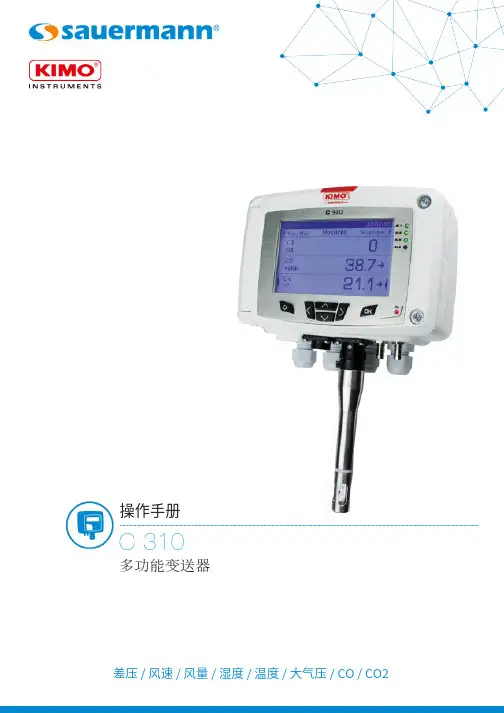
差压 / 风速 / 风量 / 湿度 / 温度 /大气压 / CO / CO2操作手册C 310多功能变送器0 / 4 ~ 20 m A - 电流输出信号接线端口 (a)电源供应 (c)电缆接入电源种类(a)模拟输出 (1)0 ~ 5 / 10 V - 电压G N D - 接地差压自动校准元件压力连接端口智能型探头连接端口差压或大气压模块差压手动零点校准以太网通讯模块总线通讯RS 485 (d)继电器 (b)N OC O MN C(b)继电器 (1)N OC O MN C继电器 (4)N OC O MN C继电器 (3)N OC O MN C继电器 (2)0 / 4 ~ 20 m A - 电流模拟输出 (4)0 ~ 5 / 10 V - 电压G N D - 接地0 / 4 ~ 20 m A- 电流模拟输出 (3)0 ~ 5 / 10 V- 电压G N D - 接地0 / 4 ~ 20 m A - 电流模拟输出 (2)0 ~ 5 / 10 V - 电压G N D - 接地(c)用于电源供应相位 中性 (c)用于电源供应相位 中性 (d)Modbus RS-485ABC 310 接线图电气接线 - 符合 NFC15-100 标准接线应由合格技术人员操作。
当接线时, 变送器必须停止供应电源。
➢电流输出信号 0 / 4 ~ 20 mA 接线方式:➢电源供应 24 Vdc 接线方式:➢电源供应 24 Vac 接线方式:➢电源供应 230 Vdc 接线方式:电源供应 24 Vac Class II显示仪 或 PLC / BMS主动种类+-24 Vdc电源供应+-N LLN Pe 230 VacLN Pe 230 Vac或LN LN LN 24 VacLN 230 Vac电源供应GND-+显示仪 或 PLC / BMS主动种类-+GNDL N 24 Vac电源供应 24 Vac Class II➢电压输出信号 0 ~ 5 / 10 V 接线方式:内容目录1. 产品介绍 (5)1.1 变送器介绍 (5)1.2 按键介绍 (5)1.3 温湿度传感器保护盖 (6)2. Modbus 通讯 (7)2.1 设置参数 (7)2.2 功能 (7)2.3 寄存器读取码 (7)3. 设置变送器 (12)3.1 输入安全码 (12)3.2 设置变送器的参数 (12)3.2.1 设置显示屏 (13)3.2.2 设置曲线图时段 (13)3.2.3 设置语言 (13)3.2.4 设置日期和时间 (13)3.2.5 开启/关闭按键音 (13)3.2.6 锁定或开启按键 (13)3.2.7 修改安全码 (14)3.2.8 恢复出厂设置 (14)3.2.9 设置Modbus通讯 (适用于已订购此功能) (14)3.2.10 设置以太网通讯 (适用于已订购此功能) (14)3.2.11 访问变送器信息 (15)3.3 设置测量通道 (15)3.4 设置模拟信号输出 (15)3.4.1 选择模拟信号输出类型 (15)3.4.2 设置模拟信号输出对应量程 (16)3.4.3 输出信号自诊断 (16)3.5 设置报警 (17)3.5.1 选择报警模式 (17)3.5.2 设置上升或下降报警模式 (18)3.5.3 设置监测报警模式 (18)3.5.4 设置变送器状态报警模式 (19)3.5.5 设置继电器 (适用于已订购此功能) (19)3.6 设置探头, 模块和标准参数 (20)3.6.1 设置风速和风量探头 (20)3.6.2 设置二氧化碳或温湿度探头 (21)3.6.3 设置模块 (21)3.7 开启其他选购功能 (24)4. 功能描述和 Modbus 通讯连接 (26)4.1 变送器 (26)4.2 测量通道 (27)4.3 输出信号 (27)4.4 报警和继电器 (28)4.4.1 报警 (28)4.4.2 继电器 (29)4.5 测量参数 (29)4.6 差压模块和探头 1 和 2 参数 (30)4.6.1 差压模块参数 (30)4.6.2 探头 1 参数 (31)4.6.3 探头 2 参数 (31)4.6.4 标准参数 (32)1. 产品介绍1.1变送器介绍C310 变送器含显示屏型号可通过按键进行设置。

目录第一章 综述 (1)1.1安全注意事项 (1)1.2使用前 (1)1.3技术规范 (3)第二章 安装 (5)第三章 键盘布局及操作说明 (11)第四章 参数表 (13)4.1参数图标说明 (13)4.2参数一览表 (13)4.3F00组:环境应用 (14)4.4F01组:基本设定 (15)4.5F02组:电机1参数 (18)4.6F03组:矢量控制 (21)4.7F04组:V/F控制 (24)4.8F05组:输入端子 (26)4.9F06组:输出端子 (30)4.10F07组:运行控制 (34)4.11F08组:辅助控制 (36)4.12F09组:辅助控制2 (37)4.13F10组:保护参数 (37)4.14F11组:键盘参数 (41)4.15F12组:通信参数 (43)4.16F13组:过程PID控制 (46)4.17F14组:多段速及简易PLC (48)4.18F15组:保留 (51)4.19F16组:张力控制 (51)4.20F25组:AI及AO校正 (55)4.21C0X组:监控参数 (55)4.22端子输入输出功能选择 (57)4.23故障及警告代码表 (58)第五章 检查、维护与保证 (60)5.1检查 (60)5.2维护 (61)5.3产品保证 (61)附录一: MODBUS通信协议 (62)附录二: 端子接线方式 (64)附录三: 外引键盘尺寸及型号 (65)第一章综述1.1 安全注意事项为保证安全、合理的使用本产品,请在完全理解本手册所述的安全注意事项后再使用该产品。
警示标志及其含义本手册中使用了下列标记,表示该处是有关安全的重要内容。
如果不遵守这些注意事项,可能会导致人身伤亡、本产品及关联系统损坏。
危险:如果操作错误,可能会造成死亡或重大安全事故。
注意:如果操作错误,可能会造成轻伤。
操作资质本产品必须由经过培训的专业人员进行操作。
并且,作业人员必须经过专业的技能培训,熟悉设备的安装、接线、运行和维护保养,并正确应对使用中出现的各种紧急情况。

Table of ContentsPrefaceAbout this User's Guide (4)What you will learn from this user's guide (4)Conventions in this user's guide (4)Where to find more information (4)Chapter 1Introducing the OM-USB-3103 (5)Functional block diagram (5)Chapter 2Installing the OM-USB-3103 (6)What comes with your shipment? (6)Hardware (6)Software (6)Documentation (6)Unpacking (6)Installing the software (6)Installing the hardware (6)Calibrating the OM-USB-3103 (7)Chapter 3Functional Details (8)External components (8)USB connector (8)LED indicators (8)Screw terminals (8)Signal connections (9)Analog voltage outputs (9)Digital I/O (9)Digital I/O control terminal (DIO CTL) for pull-up/down configuration (9)Synchronous DAC load terminal (SYNCLD) (10)Counter input (10)Power output (10)Ground (10)Chapter 4Specifications (11)Analog voltage output (11)Analog output calibration (12)Digital input/output (12)Synchronous DAC Load (13)Counter (13)Memory (14)Microcontroller (14)Power (14)USB specifications (14)Environmental (14)Mechanical (14)Main connector and pinout (15)About this User's GuideWhat you will learn from this user's guideThis user's guide describes the Omega Engineering OM-USB-3103 data acquisition device and lists device specifications.Conventions in this user's guideCaution!Shaded caution statements present information to help you avoid injuring yourself and others, damaging your hardware, or losing your data.bold text Bold text is used for the names of objects on a screen, such as buttons, text boxes, and check boxes.italic text Italic text is used for the names of manuals and help topic titles, and to emphasize a word or phrase.Where to find more informationAdditional information about OM-USB-3103 hardware is available on our website at . You can also contact Omega Engineering by phone, fax, or email with specific questions.▪Phone: (203) 359-1660▪Fax: (203) 359-7700▪Email: *************Introducing the OM-USB-3103The OM-USB-3103 is a USB 2.0 full-speed device that is supported under popular Microsoft® Windows®operating systems. The OM-USB-3103 is fully compatible with both USB 1.1 and USB 2.0 ports.The OM-USB-3103 provides eight channels of analog voltage output, eight digital I/O connections, and one 32-bit event counter.The OM-USB-3103 has two quad (4-channel) 16-bit digital-to-analog converters (DAC). You set the voltage output range of each DAC channel independently with software for either bipolar or unipolar. The bipolar range is ±10 V, and the unipolar range is 0 to 10 V. The analog outputs may be updated individually orsimultaneously. A bidirectional synchronization connection allows you to simultaneously update the DAC outputs on multiple devices.The OM-USB-3103 features eight bidirectional digital I/O connections. You can configure the DIO lines as input or output in one 8-bit port. All digital pins are floating by default. A screw terminal connection isprovided for pull-up (+5 V) or pull-down (0 volts) configuration.The 32-bit counter can count TTL pulses.The OM-USB-3103 is powered by the +5 volt USB supply from your computer. No external power is required.All I/O connections are made to screw terminals.Functional block diagramOM-USB-3103 functions are illustrated in the block diagram shown here.Figure 1. OM-USB-3103 block diagramInstalling the OM-USB-3103What comes with your shipment?The following items are shipped with the OM-USB-3103:Hardware▪OM-USB-3103▪USB cableSoftware▪Software for OMB-DAQ-2400, OM-USB, OM-WEB, and OM-WLS Series Data Acquisition Modules CD DocumentationIn addition to this hardware user's guide, you should also receive the OMB-DAQ-2400, OM-USB, OM-WEB, and OM-WLS Series Data Acquisition Software User's Guide. This booklet provides an overview of thesoftware you received with the device, and includes information about installing the software.UnpackingAs with any electronic device, take care while handling to avoid damage from static electricity. Beforeremoving the device from its packaging, ground yourself using a wrist strap or by simply touching the computer chassis or other grounded object to eliminate any stored static charge.If any components are missing or damaged, notify Omega Engineering immediately by phone, fax, or e-mail.▪Phone: (203) 359-1660▪Fax: (203) 359-7700▪Email: *************Installing the softwareRefer to the Software User's Guide for instructions on installing the software. This booklet ships with the hardware, and is available in PDF at /manuals/manualpdf/M4803.pdf..Installing the hardwareTo connect the OM-USB-3103 to your system, connect the USB cable to an available USB port on thecomputer or to an external USB hub connected to the computer. Connect the other end of the USB cable to the USB connector on the device. No external power is required.When connected for the first time, a Found New Hardware dialog opens when the operating system detects the device. When the dialog closes, the installation is complete. The LED on the OM-USB-3103 turns on after the device is successfully installed.OM-USB-3103 User's Guide Installing the OM-USB-3103Calibrating the OM-USB-3103The OM-USB-3103 is shipped fully calibrated. Calibration coefficients are stored in the device FLASHmemory. Return the device to Omega Engineering when calibration is required. The normal calibration interval is once per year.Chapter 3 Functional DetailsExternal componentsThe OM-USB-3103 has the following external components, as shown in Figure 2.▪Screw terminals▪LED indicators▪USB connector1 Screw terminal pins 1 to 28 4 Power LED2 Screw terminal pins 29 to 56 5 USB connector3 Status LEDFigure 2. OM-USB-3103 external componentsUSB connectorThe USB connector provides power and communication. The voltage supplied through the USB connector is system-dependent, and may be less than 5 V. No external power supply is required.LED indicatorsThe OM-USB-3103 has two LED indicators –Status and Power.▪The Status LED indicates the communication status of the OM-USB-3103. It blinks when data is being transferred, and is off when the OM-USB-3103 is not communicating. This LED uses up to 10 mA ofcurrent and cannot be disabled.▪The Power LED turns on when the device is connected to a USB port on a computer or an external USB hub connected to a computer.Screw terminalsThe screw terminals on the bottom edge of the OM-USB-3103 provide the following connections:▪Eight analog voltage outputs (VOUT0 through VOUT7)▪Eight digital I/O (DIO0 to DIO7)▪One digital I/O pull-down resistor connection (DIO CTL)▪One SYNC I/O terminal for external clocking and multi-unit synchronization (SYNCLD)▪One counter input (CTR)▪One power output (+5 V)▪Analog ground (AGND) and digital ground (DGND) connectionsFigure 3. OM-USB-3103 signal pinoutUse 16 AWG to 30 AWG wire gauge when making screw terminal connections.Signal connectionsAnalog voltage outputsThe screw terminal pins labeled VOUT0 to VOUT7 are voltage output terminals. The voltage output range for each channel is software-programmable for either bipolar or unipolar. The bipolar range is ±10 V, and the unipolar range is 0 to 10 V. The channel outputs may be updated individually or simultaneously.Digital I/OYou can connect up to eight digital I/O lines to DIO0 through DIO7. Each digital channel is individuallyconfigurable for input or output. The digital I/O terminals can detect the state of any TTL-level input. Refer to the schematic shown in Figure 4.Figure 4. Schematic showing switch detection by digital channel DIO0 If you set the switch to the +5 V input, DIO0 reads TRUE (1). If you move the switch to DGND, DIO0 reads FALSE (0).Digital I/O control terminal (DIO CTL) for pull-up/down configurationAll digital pins are floating by default. When inputs are floating, the state of unwired inputs are undefined (they may read high or low). You can configure the inputs to read a high or low value when they aren’t wired. Use the DIO CTL pin to configure the digital pins for pull-up (inputs read high when unwired) or pull-down (inputs read low when not wired).▪To pull up the digital pins to +5V, wire the DIO CTL terminal pin to the +5V pin.▪To pull down the digital pins to ground (0 volts), wire the DIO CTL terminal pin to a DGND pin. Synchronous DAC load terminal (SYNCLD)The synchronous DAC load connection is a bidirectional I/O signal that allows you to simultaneously update the DAC outputs on multiple devices. You can use this pin for two purposes:▪Configure as an input (slave mode) to receive the D/A LOAD signal from an external source.When the SYNCLD pin receives the trigger signal, the analog outputs are updated simultaneously.▪Configure as an output (master mode) to send the internal D/A LOAD signal to the SYNCLD pin.You can use the SYNCLD pin to synchronize with a second OM-USB-3103 and simultaneously update the DAC outputs on each device. Refer to Synchronizing multiple units section below.Use InstaCal to configure the SYNCLD mode as master or slave. On power up and reset the SYNCLD pin is set to slave mode (input). Refer to the "USB-3100 Series" section in the Universal Library User's Guide for information on how to configure the OM-USB-3103 with the Universal Library.Synchronizing multiple unitsYou can connect the SYNCLD terminal pin (pin 49) of two OM-USB-3103 units together in a master/slave configuration and simultaneously update the DAC outputs of both devices. Perform the following procedure:1.Connect SYNCLD on the master OM-USB-3103 to the SYNCLD pin on the slave OM-USB-3103.2.Configure SYNCLD on the slave device for input to receive the D/A LOAD signal from the master device.Use InstaCal to set the direction of the SYNCLD pin.3.Configure SYNCLD on the master device for output to generate an output pulse on the SYNCLD pin.Set the Universal Library SIMULTANEOUS option for each device. Refer to the Universal Library User's Guide for information on how to configure the OM-USB-3103 with the Universal Library. When the SYNCLD pin on the slave device receives the signal, the analog output channels on each device are updated simultaneously. Counter inputThe CTR terminal is a 32-bit event counter that can accept frequency inputs up to 1 MHz. The internal counter increments when the TTL levels transition from low to high.Power outputThe +5V terminal can output up to 10 mA maximum. You can use this terminal to supply power to external devices or circuitry.Caution!The +5V terminal is an output. Do not connect to an external power supply or you may damage the device and possibly the computer.GroundThe analog ground (AGND) terminals provide a common ground for all analog voltage output channels.The digital ground (GND) terminals provide a common ground for the digital, counter, and sync terminal and the power terminal.Chapter 4 SpecificationsTypical for 25 °C unless otherwise specified.Specifications in italic text are guaranteed by design.Analog voltage outputTable 1. Analog voltage output specificationsNote 1: The OM-USB-3103 output voltage level defaults to 0 V whenever the output voltage range is reconfigured.The OM-USB-3103 output voltage level will also default to 0 V:1) Whenever the host PC is reset, shut down or suspended.2) If a reset command is issued to the device.Note 2: The duration of this particular output transient is highly dependent on the enumeration process of the host PC. Typically the output of the USB-3103 is stable after 2 seconds.Note 3: The maximum differential non-linearity specification applies to the entire 0 to 70 °C temperature range of the OM-USB-3103. This specification also accounts for the maximum errors due to thesoftware calibration algorithm (in Calibrated mode only) and the DAC8554 digital to analogconverter non-linearities.Table 2. Absolute accuracy specifications – calibrated outputTable 3. Absolute accuracy components specifications – calibrated outputTable 4. Relative accuracy specificationsAnalog output calibrationTable 5. Analog output calibration specificationsDigital input/outputTable 6. Digital I/O specificationsNote 4: Pull up and pull down configuration area available using the DIO CTL terminal block pin 54.The pull down configuration requires the DIO CTL pin (pin 54) to be connected to a DGND pin(pin 50, 53 or 55). For a pull up configuration, the DIO CTL pin should be connected to the +5 Vterminal pin (pin 56).Synchronous DAC LoadTable 7. SYNCLD I/O specificationsNote 5: SYNCLD is a Schmitt trigger input and is over-current protected with a 200 Ohm series resistor.Note 6: When SYNCLD is in input mode, the analog outputs may either be updated immediately or whena positive edge is seen on the SYNCLD pin (this is under software control.) However, the pinmust be at a low logic level in order for the DAC outputs to be updated immediately. If anexternal source is pulling the pin high, no update will occur.CounterTable 8. CTR I/O specificationsMemoryTable 9. Memory specificationsMicrocontrollerTable 10. Microcontroller specificationsPowerTable 11. Power specificationsNote 7: This is the total quiescent current requirement for the OM-USB-3103 which includes up to10 mA for the status LED. This does not include any potential loading of the digital I/O bits,+5 V user terminal, or the VOUTx outputs.Note 8: Output voltage range assumes USB power supply is within specified limits.Note 9: This refers to the total amount of current that can be sourced from the +5 V user terminal (pin 56) for general use. This specification also includes any additional contribution due to DIO loading. USB specificationsTable 12. USB specificationsEnvironmentalTable 13. Environmental specificationsMechanicalTable 14. Mechanical specificationsMain connector and pinoutTable 15. Main connector specifications。
D A C数字模拟转换器参考手册中文版11 DAC 简介Naim DAC 数字到模拟转换器是一款高度通用的产品,我们强烈建议您阅读本手册。
此外,您还应该阅读随产品一同提供的法定和通用信息手册,因为其包含重要的关于主电源的安全警告。
DAC 可以具有多个电力供应升级选项。
请联系当地零售商或分销商获得关于电源升级选择的意见。
本手册中关于Naim 前置扩音器的说明也涵盖了Naim 集成扩音器的前置扩音器部件。
1.2 DAC 基本知识Naim DAC 是能够处理8位至32位分辨率、32kHz 至768kHz 采样率的立体声音频数据的输入数字到模拟转换器。
其立体声模拟输出可通过DIN 或RCA 唱机插座获得。
8个DAC 数字输入可通过后面板上的光纤或同轴S/PDIF 输入插座进行访问,按前面板的输入选择按钮之一可以选中该些输入插座。
另外两个数字输入可以通过USB 接口进行访问;一个输入在前面板上,另一个输入在后面板上。
USB 接口可用于连接载有音频文件的USB 记忆棒或苹果iPod 或iPhone 机型。
USB 设备连接后,USB 接口会自动被选中。
USB 设备连接后,其所载音频文件可以通过DAC 进行播放。
DAC 前面板的插入对接按钮指示灯将变亮,输入选择按钮可作为“上一曲目”、“下一曲目”、“停止”和“播放”按钮进行操作。
断开USB 设备连接或按插入对接按钮,DAC 将返回至S/PDIF 输入操作。
然后,最后使用过的S/PDIF 输入将被选中。
DAC 可以从其前面板按钮或使用在前置扩音器模式下的Naim 遥控器进行控制。
也可以用苹果遥控器来控制播放和音量。
22.2 S/PDIF 输入带有连接格式和插座选项的8个后面板S/PDIF 输入。
该些输入在下表列出:输入 光纤插座 同轴插座 S/PDIF 1 TOSLINK BNC (75Ω) S/PDIF 2 TOSLINK BNC (75Ω) S/PDIF 3 TOSLINK RCA 唱机 S/PDIF 4TOSLINKRCA 唱机每个输入端一次仅可使用一种连接格式(光纤或同轴)。
以下是FCA3103使用手册的概述:
1. 概述
FCA3103是一款高性能的数字信号分析仪,能够提供多种测量功能,包括频谱分析、谐波测量、相位测量等。
FCA3103具有低功耗、高精度和易于使用等特点,适合于各种应用场景。
2. 安装和配置
要使用FCA3103,需要按照以下步骤进行安装和配置:
-连接FCA3103到计算机上,并安装驱动程序和软件。
-配置FCA3103的参数,包括测量范围、采样率、触发模式等。
-根据实际需要配置FCA3103的输入和输出接口,包括ADC、DAC和GPIO等。
3. 使用说明
使用FCA3103时,需要注意以下几点:
-打开FCA3103的软件界面,选择需要使用的功能和参数。
-根据实际需要进行数据采集和分析,可以使用FCA3103的内置分析工具或自定义算法。
-根据实际需要进行数据存储和导出,可以使用FCA3103的内置存储功能或外部存储设备。
-进行数据备份和恢复等操作,以确保数据的安全性和完整性。
4. 常见问题和解决方案
在使用FCA3103时,可能会遇到一些常见问题,例如无法启动、测量不准确、数据丢失等。
为了解决这些问题,需要查阅FCA3103的官方文档或在线社区,或者联系FCA3103的技术支持团队。
以上是FCA3103使用手册的概述,如果需要更详细的操作指南,请查阅FCA3103的官方手册或在线教程。
中楼310,405,404新配备了蓝鸽语音设备,教研室大部分老师参加了操作培训,以下是章老师所做笔记,我打出来发给大家,希望能对大家有所帮助.感谢章老师!如果其他老师还有补充,也请发至本邮箱.蓝鸽语音设备操作说明Great Wall:罗师傅Tele:6128081打开总电源,电脑电源后点击数字网络语音室系统直接进入课堂教学(教师选入)点确定+PC界面…但是自主学习(是默认的)‟:(如果用教学光碟,缩小原窗口,再装碟,先点击光碟安装,然后再点击最下方的四方框)①广播(全通话)、对讲(红色开、黑色关)②广播+对讲=示范点击一个学生③(取消广播)对讲=单独师生对话④多人对讲:广播+小组+对讲点击位置⑤(小组下)固定分组,数字相同一个组⑥随机抓人为一组,要先自己告诉对方是谁本地库:(教材正用自己带磁带、光盘、用本地库直接上课。
)外设:(可以把磁带放进,在界面上操作。
)分班:(可以播不同的听力资料,用鼠标框选,按照几个组放不同的资料听,取消,点击分班即可。
)检测:点击,看每个位置下是否有红线,没有就会发现是否主机出现问题,再找如:音量的大小,耳机没插,显示器亮度关了。
只要是绿色灯,就是亮度和对比度关了,黄灯就是出了故障。
PC界面:出现桌面,如平时操作。
不带病毒,建议把教学资料拷贝到D盘“某老师的文件”教案录制:(是否要保存整堂课的录音,可以按是)如是随堂课可删除。
学生录音:点击随堂口语录音,可以收听。
可以进行随堂测试,马上录音,马上看结果,可在本地库查到每个人录音。
右边是操纵左边是监视放磁带:外设放磁带时,要打开广播放影碟:开仓,打开公放,音量的加减在操作屏中间放视频:播音+PC界面放视频开总开关从大到小――开电脑上的power――进入数字网络语言――课堂教学――确定――PC 界面――开学生开关。
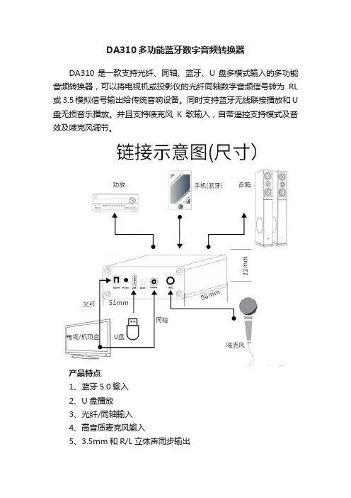
DA310多功能蓝牙数字音频转换器DA310是一款支持光纤、同轴、蓝牙、U盘多模式输入的多功能音频转换器,可以将电视机或投影仪的光纤同轴数字音频信号转为RL 或3.5模拟信号输出给传统音响设备。
同时支持蓝牙无线联接播放和U 盘无损音乐播放。
并且支持唛克风K歌输入,自带遥控支持模式及音效及唛克风调节。
产品特点1、蓝牙5.0输入2、U盘播放3、光纤/同轴输入4、高音质麦克风输入5、3.5mm和R/L立体声同步输出6、遥控器控制选择U盘:绿灯常亮;光纤:红灯常亮;同轴:绿白常亮蓝牙:蓝色闪烁(配对状态),蓝色常亮(已联接)蓝牙连接1、装上标配天线,接通电源,拨动开关,按遥控器选择蓝牙模式,接收器会进入配对状态,指示灯蓝灯快闪。
2 、打开手机/平板等设备的蓝牙功能-点击搜索。
3、选择蓝牙名:DA310,选择配对连接,连接上蓝牙后蓝灯常亮;。
4、转换器会在下次开机自动回联最后配对设备。
同轴/光纤连接:将电视机&投影仪的同轴或光纤输出口与DA310设备对应输入接口联接,将电视等设备音源修改同轴或光纤输出,格式调整为PCM。
当音源输入后,用DA310标配遥控可选择任一对应功能。
U盘播放:1 、选择32G以下U盘,将U盘格式化为FTA32,并拷入相应音乐(MP3、WAV、WMA、APE、FLAC等格式)2、接入U盘,用遥控器选择U盘模式即可以播放。
U盘播放绿灯常亮;唛克风输入:DA310支持唛克风输入,直接将有线或无线电容唛克风插入MIC 接口,即可以将唛克风声音与任何音频输入信号叠加,在家即可以K 歌。
产品接口介绍1:光纤输入口2:指示灯3:USB输入 4:同轴输入 5:麦克风输入(6.5MM)6:3.5MM输出口 7:RCA输出口 8:开关 9:电源接口 10:蓝牙天线READ为摇控器接收窗口产品参数:产品型号……………DA310电源输入……………5V 1000mA蓝牙版本……………蓝牙5.0蓝牙协议……………A2DP, AVRCP,PBAPU盘输入……………FAT32 up 32G音乐格式……………MP3、WAV、WMA、APE、FLAC 信噪比………………≥90dBDAC SNR……………96dB频率响应……………20HZ- 20khz采样率………………8,11.025,12,16,22.05,32,44.1 and48KHz产品净重……………114g音效模式顺序………流行、摇滚、爵士、古典、乡村常见问题与解决方案不能开机·选择合格的适配器通电,推荐选择输出电压为5V 1A适配器(务必不要使用可变电压的快充充电)。

Product InformationTriplett Corporation'sModel 310-CThe Model 310 Series is the favorite hand-held Analog VOM in theMaintenance and Telecommunications field.18 Ranges5 DC Voltage Ranges5 AC Voltage Ranges4 DC Current Ranges4 Resistance RangesPolarity Reversing SwitchDrop Resistant High-Impact CaseDiode Overload Protection with fused Resistance RangesSingle Enclosed Range SwitchSpecificationsDC VOLTAGE:RANGES: 0-3, 12, 60, 300, 600, (20,000 Ohms perVolt)ACCURACY: ± 3% of Full ScaleAC VOLTAGE:RANGES: 0-3, 12, 60, 300, 600 (15,000 Ohms perVolt)ACCURACY: ± 4% of Full ScaleRESISTANCE:RANGES: 0-20K Ohms, 200K Ohms, 2M Ohms, 20MOhms (200 Ohms center scale on lowest range)ACCURACY: ± 3% of Scale LengthDC CURRENT:RANGES: 600uA, 6mA, 60mA, 600mAMAX. VOLTAGE DROP: 330mV ACCURACY: ± 3%of Full ScaleDIMENSIONS: 2 3/4" x 1 5/16" x 4 1/4" (70mm x 33.5mm x 108mm)BATTERIES:(1) 15V NEDA #220, (1) 1.5V NEDA #910F and 12V #23ASHIPPING WEIGHT: 2 lbs. (1kg.)ACCESSORIES INCLUDE:42" safety test leads, screw-on insulated alligator clips, batteries and instruction manual.AccessoriesCatalog No.Description10-125869 Carrying Case - Trouser Belt Pouch for 310 Series10-1456379 Carrying Case - Designed to hold the Model 100 Series10-1608369-T Carrying Case with Neck Strap for hand-free use 10-1791369-S Carrying Case - Flap folds back to form stand 10-2959369V Carrying Case - padded black vinyl pouch10-2969Carrying Case with Belt Loop37-21 1.5 Volt Battery37-2215 Volt Battery (310 Series Type 5 & earlier)37-6012 Volt Battery (310 Series Type 6 & 7)60-211Model 10 Clamp-On (310, 310-TEL & 100)60-218Model 101 Line Separator60-335Model 10-C Clamp-On (310-C & 100-C)60-535Model 10-E Clamp-On (Export-50Hz)79-15342" Test Leads for 310 Series79-206Test Leads with alligator clips (no probes)79-414Replacement Bar Lead for Model 1079-41642" Separating Leads (310 Series to Model 10 Series) 79-695Test Lead with pin cushion clip79-722Test Lead with spike clip3207-371/16 A Fuse (310 Series Type 6 & earlier)3207-1121/16 A Fuse (310 Series Type 7 only)。
D A C310系统在剪板机系统中是一种经济实用的数控系统,在广大客户中使用的口碑也非常不错,具体的功能和作用也不用多说,下来主要说一下系统调试和故障解决。
一、系统调试步骤在对剪板机进行调试之前,必须仔细阅读D A C310安装手册及接线图,了解各I/O口的功能、设计电路。
了解各机械结构的性能及动作要求。
基本检查和调试步骤可参考如下:1、 根据电路原理图,仔细检查电柜内的接线及外部接线,确认接线正确、牢固、接地线可靠。
2、 关闭总电源开关、断路器开关,并折下与D A C310连接的所有接头,同时,折下后挡料电机与机架的机械联接。
3、 接上总电源、测量三相输入电压是否平衡。
电压稳态值为0.9~1.1倍额定电压。
若自备发电机组必须加稳压滤波器。
4、 闭合各级电源开关,检查各电源是否正常。
5、 在确认电源都正常后,断开总电源,重新联接好与系统联接的插头。
6、 接通系统电源,根据系统安装手册对数控系统的机床参数进行设置。
7、 接通伺服电源(为了安全,此时伺服电机必须未与机架联接),设置有效的参数后对后挡料伺服进行编程参数设定,使其满足基本动作要求。
8、 将数控系统调到手动状态,用手动方式,使电机正反向运转,确定前后限位开关是否有效,编码器计数方向是否正确,R S D开关是否有效等。
9、 在确认系统计数方向前后限位都正常后,将后挡料的机械联接机构装上。
10、示教模式下(13I n d e x i n g设为0),直接输入当前后挡料的实际位置,编辑一定距离的后挡料位移量,用卡尺测量后挡料实际移动的距离与编程的值是否一致,如果不一致修改系统参数或驱动参数直到一致;11、寻参模式下(13I n d e x i n g设为1),将参考点的值输入,编辑1个小于参考点的位置后并运行, 测量X编程值与实际值的差,修正X轴参考点值,直到X编程与实际值一致为止。
12、后挡料定位调试完成后,调试机床单次、连续动作是否正常,剪切延时是否正常等;13、编辑一个多步程序运行后检查系统的换步信号,计数信号是否正常。
DAC-310第一部分系统I/O输入输出信号第二部分系统诊断功能第三部分系统参数理解第四部分系统调试与常见故障分析系统输入/输出定义DAC-310 控制器拥有输入/输出可编程的特性,可以通过软件设定将系统信号映射到输入/输出端子上。
进入输入/输出定义界面的方法:1:将贯标移动到参数M 上;2:输入密码963,然后按回车。
系统显示如下图所示:每一个选项都显示系统的内部逻辑信号和可用端子组成的矩阵,数字输入子项的显示如下图所示:在屏幕的顶部显示可用的端子,在屏幕的左侧显示系统内部的逻辑信号,信号和端子仪如下方式联系在一起:1:使用上、下箭头键和±键将光标移动到需要的交叉点上;2:按Enter 键确认。
D1—D4 指DAC 310控制器的4 个数字输入;0 是逻辑常量FALSE,1 是逻辑常量TRUE。
如果一个内部信号与FALSE 联系在一起,系统将会认为该信号始终为低(不起作用);反之,系统认为该信号始终为高(有效)。
数字输出的设定方法与之相似。
系统输出时,多个逻辑信号可以输出在同一个端子上,这些逻辑信号进行“与”操作:即一个或多个信号有效后,该端子就输出高电平。
输入/输出列表数字输出信号:代码名称描述:R 退让输入退让输入信号ST 换步输入外部启动信号,用于使能轴的移动和换步。
RSD 参考点输入:如果寻参过程中使用了参考点开关,该端子就是后挡料参考点开关的输入KEY 编程锁该信号用于使能/禁止控制器的编程操作RFC 参考校正位置校正输入数字输入信号:输出信号代码名称描述:RDY 准备好系统准备就绪,即控制器结束定位操作。
如用于剪板机,后挡料到位且刀口间隙到位后,该信号输出高电平。
EOC 循环结束程序或工步执行完成。
EOS 剪程结束剪程结束,剪切位置到或延时时间到F1 功能输出1 通用可编程输出F2 功能输出2 通用可编程输出G+ 间隙增大增大刀口间隙G- 间隙减小减小刀口间隙+ Opening AC电机正向命令- Closing AC电机反向命令++ Fast Opening AC电机快速正向命令-- Fast Closing AC电机快速反向命令BRK 抱闸信号为配备抱闸系统的AC电机提供抱闸信号,该信号是“低电平有效”:即定位过程中该信号保持为高;应用抱闸系统时该信号为低。
User's GuideSBOU096A–November2010–Revised January2011DAC31x2EVM This document is a user's guide for the DAC31x2EVM,an evaluation fixture for the DAC3152and DAC3162(DAC31x2)series of dual-channel,10-/12-bit,500-MSPS digital-to-analog converters(DACs).The DAC31x2EVM includes the TRF3703-33quadrature modulator to facilitate measuring the output signals at a desired RF frequency.The EVM also includes the CDCP1803clock buffer that distributes the clocks to the DAC,as well as a pattern generator.This EVM is ideally suited for mating with the TSW3100 pattern generation card for evaluating QAM,WCDMA,LTE,or other high-performance modulation schemes.For more information about the DAC31x2family,see the product data sheet(available for download at ).Throughout this document,the acronym EVM and the phrases evaluation module and evaluation fixture are synonymous with the DAC31x2EVM.Contents1Introduction (2)2Testing and Configuration (3)List of Figures1DAC31x2EVM Block Diagram (2)2DAC31x2EVM Test Setup (3)3TSW3100CommsSignalPattern(WCDMA)Programming GUI (4)4DAC3162EVM and TRF3703-33WCDMA Output (5)5DAC3162EVM Transformer-Coupled Output at30MHz IF (6)All trademarks are the property of their respective owners.1 SBOU096A–November2010–Revised January2011DAC31x2EVM Submit Documentation FeedbackRFLO (Introduction 1Introduction 1.1Block DiagramFigure 1shows the DAC31x2EVM block diagram.Figure 1.DAC31x2EVM Block Diagram1.2Software ControlNo software is required to use the DAC31x2EVM.2DAC31x2EVM SBOU096A–November 2010–Revised January 2011Submit Documentation Feedback Testing and Configuration 2Testing and ConfigurationThis section outlines the basic procedure for testing the DAC31x2EVM.2.1Test Set-UpFigure 2illustrates the test configuration for general testing of the DAC31x2with the TSW3100patterngeneration card.Figure 2.DAC31x2EVM Test Setup2.2Test Set-Up ConnectionsFollow these procedures to properly connect the DAC31x2EVM and the TSW3100pattern generator.TSW3100Pattern Generator:•Connect a 5-V power supply to J9,the 5V_IN jack of the TSW3100EVM.•Connect the PC Ethernet port to J13,the Ethernet port of the TSW3100.The cable should be astandard crossover Cat5e Ethernet cable.DAC31x2EVM:•Connect the J5connector of DAC31x2EVM to connector J74of the TSW3100EVM.•Connect 5V and Ground to connectors J12and J13respectively.•Provide a 0.5-V RMS ,500-MHz (max)clock at J9,the CLOCK IN SMA port of the DAC31x2EVM.•Provide a 7-dBm,350-MHz to 4-GHz local oscillator (LO)source at port J10of the DAC31x2EVM.Thisinput provides the LO source to the TRF3703-33modulators.•Connect the RF output port of (J11)to the spectrum analyzer.DAC31x2EVM Jumpers:Power distribution to the DAC31x2and CDCP1803devices on the EVM can be achieved throughlow-dropout regulators (LDOs)or dc-dc converters.Jumpers JP24,JP25,JP26,and JP27allow theuser to choose one of the power schemes from these two available options.The default setting ofthese jumpers is shown;these settings use power management for the ICs through dc-dc switchers.•JP24on pin {1,2}•JP25on pin {1,2}•JP26on pin {1,2}•JP27on pin {1,2}Jumper JP4supplies power to the TRF3703-33modulator.This jumper must be installed in order to usethe modulator.3SBOU096A–November 2010–Revised January 2011DAC31x2EVM Submit Documentation FeedbackTesting and Configuration 2.3TSW3100Quick-Start OperationRefer to the TSW3100User’s Guide for a more detailed discussion of how to set up and operate theTSW3100.This user guide presumes that the TSW3100software is installed and functioning properly.CommsSignalPattern Setup from Default Configuration(WCDMA):Step1.Change the interpolation value to DAC Clock Rate/3.84(that is,491.52/3.84=128).Step2.Enter the desired offset frequency(for example,30MHz)for each desired carrier.Step3.Select the LVDS Output button.Step4.Select the Offset Binary option.Step5.Check the LOAD and Run box.Step6.Press the green Create button.Figure3shows a screenshot of the properly configured TSW3100software interface.Figure3.TSW3100CommsSignalPattern(WCDMA)Programming GUI4DAC31x2EVM SBOU096A–November2010–Revised January2011Submit Documentation Feedback Testing and Configuration 2.4DAC31x2EVM Configuration for Modulator OutputFollow these steps to set up the DAC31x2EVM and perform a spectrum analysis.at the J9SMA connector of the DAC31x2EVM.Step1.Set the clock input to491.52MHz at0.5VRMSStep2.Supply the LO source of900MHz(7dBm)at the J10SMA connector of the DAC31x2EVM.Step3.Turn on power to the board at J12/J13.Step4.Verify the spectrum using the Spectrum Analyzer at the RF output of the DAC31x2EVM (J11).A typical WCDMA output from a wave analyzer is shown in Figure4.Figure4.DAC3162EVM and TRF3703-33WCDMA Output5 SBOU096A–November2010–Revised January2011DAC31x2EVM Submit Documentation FeedbackTesting and Configuration 2.5DAC31x2EVM Configuration for DAC OutputFollow this procedure to configure the DAC31x2EVM in order to test the EVM signal output.Step1.Four0-Ωresistors must be moved in order to configure the output of the DAC31x2as1:1 transformer-coupled.•Remove the resistors R109,R110,R111,and R112•Install the resistors R211,R207,R191,and R195Step2.Provide the clock input:491.52MHz at1.5VRMS at the J9SMA connector of theDAC31x2EVM.Step3.Turn on power to the board at J12/J13.Step4.Verify the spectrum using the Spectrum Analyzer at the two DAC outputs of theDAC31x2EVM(J3and J2).Figure5illustrates a typical transformer-coupled output using a wave analyzer.Figure5.DAC3162EVM Transformer-Coupled Output at30MHz IF6DAC31x2EVM SBOU096A–November2010–Revised January2011Submit Documentation Feedback Revision HistoryRevision HistoryChanges from Original(November,2010)to A Revision Page •Updated abstract to reflect device availability;removed DAC3172from associated devices (1)•Updated title of Figure4 (5)•Changed title of Figure5 (6)NOTE:Page numbers for previous revisions may differ from page numbers in the current version.7 SBOU096A–November2010–Revised January2011Revision History Submit Documentation FeedbackEvaluation Board/Kit Important NoticeTexas Instruments(TI)provides the enclosed product(s)under the following conditions:This evaluation board/kit is intended for use for ENGINEERING DEVELOPMENT,DEMONSTRATION,OR EVALUATION PURPOSES ONLY and is not considered by TI to be a finished end-product fit for general consumer use.Persons handling the product(s)must have electronics training and observe good engineering practice standards.As such,the goods being provided are not intended to be complete in terms of required design-,marketing-,and/or manufacturing-related protective considerations, including product safety and environmental measures typically found in end products that incorporate such semiconductor components or circuit boards.This evaluation board/kit does not fall within the scope of the European Union directives regarding electromagnetic compatibility,restricted substances(RoHS),recycling(WEEE),FCC,CE or UL,and therefore may not meet the technical requirements of these directives or other related directives.Should this evaluation board/kit not meet the specifications indicated in the User’s Guide,the board/kit may be returned within30 days from the date of delivery for a full refund.THE FOREGOING WARRANTY IS THE EXCLUSIVE WARRANTY MADE BY SELLER TO BUYER AND IS IN LIEU OF ALL OTHER WARRANTIES,EXPRESSED,IMPLIED,OR STATUTORY,INCLUDING ANY WARRANTY OF MERCHANTABILITY OR FITNESS FOR ANY PARTICULAR PURPOSE.The user assumes all responsibility and liability for proper and safe handling of the goods.Further,the user indemnifies TI from all claims arising from the handling or use of the goods.Due to the open construction of the product,it is the user’s responsibility to take any and all appropriate precautions with regard to electrostatic discharge.EXCEPT TO THE EXTENT OF THE INDEMNITY SET FORTH ABOVE,NEITHER PARTY SHALL BE LIABLE TO THE OTHER FOR ANY INDIRECT,SPECIAL,INCIDENTAL,OR CONSEQUENTIAL DAMAGES.TI currently deals with a variety of customers for products,and therefore our arrangement with the user is not exclusive.TI assumes no liability for applications assistance,customer product design,software performance,or infringement of patents or services described herein.Please read the User’s Guide and,specifically,the Warnings and Restrictions notice in the User’s Guide prior to handling the product.This notice contains important safety information about temperatures and voltages.For additional information on TI’s environmental and/or safety programs,please contact the TI application engineer or visit /esh.No license is granted under any patent right or other intellectual property right of TI covering or relating to any machine,process,or combination in which such TI products or services might be or are used.FCC WarningThis evaluation board/kit is intended for use for ENGINEERING DEVELOPMENT,DEMONSTRATION,OR EVALUATION PURPOSES ONLY and is not considered by TI to be a finished end-product fit for general consumer use.It generates,uses,and can radiate radio frequency energy and has not been tested for compliance with the limits of computing devices pursuant to part15 of FCC rules,which are designed to provide reasonable protection against radio frequency interference.Operation of this equipment in other environments may cause interference with radio communications,in which case the user at his own expense will be required to take whatever measures may be required to correct this interference.EVM Warnings and RestrictionsIt is important to operate this EVM within the input voltage range of5V to7V and the output voltage range of2.8V to3.8V. Exceeding the specified input range may cause unexpected operation and/or irreversible damage to the EVM.If there are questions concerning the input range,please contact a TI field representative prior to connecting the input power.Applying loads outside of the specified output range may result in unintended operation and/or possible permanent damage to the EVM.Please consult the EVM User's Guide prior to connecting any load to the EVM output.If there is uncertainty as to the load specification,please contact a TI field representative.During normal operation,some circuit components may have case temperatures greater than+55°C.The EVM is designed to operate properly with certain components above+55°C as long as the input and output ranges are maintained.These components include but are not limited to linear regulators,switching transistors,pass transistors,and current sense resistors.These types of devices can be identified using the EVM schematic located in the EVM User's Guide.When placing measurement probes near these devices during operation,please be aware that these devices may be very warm to the touch.Mailing Address:Texas Instruments,Post Office Box655303,Dallas,Texas75265Copyright©2011,Texas Instruments IncorporatedIMPORTANT NOTICETexas Instruments Incorporated and its subsidiaries(TI)reserve the right to make corrections,modifications,enhancements,improvements, and other changes to its products and services at any time and to discontinue any product or service without notice.Customers should obtain the latest relevant information before placing orders and should verify that such information is current and complete.All products are sold subject to TI’s terms and conditions of sale supplied at the time of order acknowledgment.TI warrants performance of its hardware products to the specifications applicable at the time of sale in accordance with TI’s standard warranty.Testing and other quality control techniques are used to the extent TI deems necessary to support this warranty.Except where mandated by government requirements,testing of all parameters of each product is not necessarily performed.TI assumes no liability for applications assistance or customer product design.Customers are responsible for their products and applications using TI components.To minimize the risks associated with customer products and applications,customers should provide adequate design and operating safeguards.TI does not warrant or represent that any license,either express or implied,is granted under any TI patent right,copyright,mask work right, or other TI intellectual property right relating to any combination,machine,or process in which TI products or services are rmation published by TI regarding third-party products or services does not constitute a license from TI to use such products or services or a warranty or endorsement e of such information may require a license from a third party under the patents or other intellectual property of the third party,or a license from TI under the patents or other intellectual property of TI.Reproduction of TI information in TI data books or data sheets is permissible only if reproduction is without alteration and is accompanied by all associated warranties,conditions,limitations,and notices.Reproduction of this information with alteration is an unfair and deceptive business practice.TI is not responsible or liable for such altered rmation of third parties may be subject to additional restrictions.Resale of TI products or services with statements different from or beyond the parameters stated by TI for that product or service voids all express and any implied warranties for the associated TI product or service and is an unfair and deceptive business practice.TI is not responsible or liable for any such statements.TI products are not authorized for use in safety-critical applications(such as life support)where a failure of the TI product would reasonably be expected to cause severe personal injury or death,unless officers of the parties have executed an agreement specifically governing such use.Buyers represent that they have all necessary expertise in the safety and regulatory ramifications of their applications,and acknowledge and agree that they are solely responsible for all legal,regulatory and safety-related requirements concerning their products and any use of TI products in such safety-critical applications,notwithstanding any applications-related information or support that may be provided by TI.Further,Buyers must fully indemnify TI and its representatives against any damages arising out of the use of TI products in such safety-critical applications.TI products are neither designed nor intended for use in military/aerospace applications or environments unless the TI products are specifically designated by TI as military-grade or"enhanced plastic."Only products designated by TI as military-grade meet military specifications.Buyers acknowledge and agree that any such use of TI products which TI has not designated as military-grade is solely at the Buyer's risk,and that they are solely responsible for compliance with all legal and regulatory requirements in connection with such use. TI products are neither designed nor intended for use in automotive applications or environments unless the specific TI products are designated by TI as compliant with ISO/TS16949requirements.Buyers acknowledge and agree that,if they use any non-designated products in automotive applications,TI will not be responsible for any failure to meet such requirements.Following are URLs where you can obtain information on other Texas Instruments products and application solutions:Products ApplicationsAudio /audio Communications and Telecom /communicationsAmplifiers Computers and Peripherals /computersData Converters Consumer Electronics /consumer-appsDLP®Products Energy and Lighting /energyDSP Industrial /industrialClocks and Timers /clocks Medical /medicalInterface Security /securityLogic Space,Avionics and Defense /space-avionics-defense Power Mgmt Transportation and /automotiveAutomotiveMicrocontrollers Video and Imaging /videoRFID Wireless /wireless-appsRF/IF and ZigBee®Solutions /lprfTI E2E Community Home Page Mailing Address:Texas Instruments,Post Office Box655303,Dallas,Texas75265Copyright©2011,Texas Instruments Incorporated。
MytekBrooklyn DAC用户手册Ver.1.2©Mytek 2016布鲁克林DAC的固件通过本公司的USB控制面板可以很容易地更新。
对于固件更新,本公司将在本公司网站“支持/下载”区发布新的固件版本部分。
固件可能改变本公司的操作细节,因此会有本手册的定期更新。
对于新闻、驱动程序更新、技术支持、提示和进一步的产品信息,请访问我们的网站:有关技术支持问题请通过我们的在线支持系统来处理。
请在本公司网站“支持/下载”区输入机器信息。
Mytek148 India St.Brooklyn, NY 11222tel. +1 (347) 384-2687目录1 简介 (5)2 包装内容 (6)3 特征 (6)4 快速入门 (7)4.1前面板 (7)4.2 后面板 (8)5 布鲁克林DAC的Windows安装和配置 (10)5.1 Windows–USB 2驱动程序的安装 (10)5.2本公司的Windows版控制面板的安装过程 (13)5.3 Windows–布鲁克林DAC播放设备的系统默认设置 (15)6 OSX版布鲁克林DAC安装 (16)6.1 OSX版USB 2驱动程序安装 (16)6.2 本公司OSX版控制面板安装 (17)7 Windows和OS X操作系统固件更新 (17)8 用户调整 (18)8.1降低输出电平 (18)9 菜单 (19)9.1菜单导航 (19)9.2菜单操作 (20)10. 遥控 (24)10.1布鲁克林DAC安装苹果遥控功能 (24)10.2布鲁克林DAC(RC5)标准的遥控设置 (25)技术指标 (25)保修 (27)重要安全信息 (27)警告 (28)废物处理的信息 (29)1简介感谢您从本公司选择布鲁克林DAC,并欢迎来到本公司的用户社区。
本公司基于掌握的20年以上转换器和其他音频设备经验,用来创建此数字到模拟转换器。
其具有尖端音频路径的设计,以提供完美,高品质,透明的声音给你的扬声器和耳机。
第一页,共一页工程名称 C H – 3 1 0 文件编号TC-T-D-23操作标准书文件名称 C H - 3 1 0 操 作 标 准版本 A310 圈 数 比 按 键 说 明□ FUNCTION MEASUTRE :测试状态。
ENTER :设定(输入)资料状态.□RATE SLOW :慢速测试.FAST :快速测试.□TRIG INT :内部自动触发测试状态.EXT/MAN :外部触发/手动触发测试状态.□NOM.V AL :标准值(参考值),按下NSN后才会显示该值.□ FREQ频率:本机有1KHz、15.7KHz、20KHz、50KHz,但要TN时按下ENTER后才可设定之,在测试时亦可变 换频率 ,再按ENTER后使用。
□ LOCK锁定键:按310LOCK锁定后重新开机不会重置(RESET)原有设定功能,开锁用同样方法即310LOCK。
□% :输入各组NS后设定%之指示灯,有1H:代表NS 1 HIGH LIMIT(高) 1L:代表NS 1 LOW LIMIT(低).□SA VE NOM :输入标准值之步骤START→SA VE→START可输入全数NS值.□ABS :绝对值,输入NOM后选定ABS可设定上限(HIGH LIMIT)值、下限(LOW LIMIT)值之实际圈数. □NSN :次级圈数组别(组数),1-9共9组(目前PCB 9组). (注:有杆子BOX可测10组).□TN :变压器规格之设定编号,从01-99共100组记忆.□VOLT :变压器一次侧供给电压,可任意选择设定从0.1-10V. (注意:310主机仅能接受10V的感应电压,故设定Vp电压以Vs不大10V为主).□TYPE :测试模式选择键NP/Ns、Vs、Ns、Sk任意选择. (Np/Ns:为初级对次级匝比,Vs:选择Vs时,以Np及Ns所 感应出之电压为显示值).□NP :在FUNCTION ENTER状态下按TYPE/NP即可设定NP之圈数值.□ENTER :输入按键.V 变更 记录 日期制 作 日 期审 核 日 期核 准 日期A 新 发 行 2000/03/01。