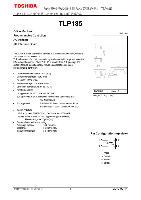
TLP152原装东芝光藕
- 格式:pdf
- 大小:184.04 KB
- 文档页数:1

东芝的高速光耦可能是全世界最齐全的一条产品线了。
300K的光耦主要是6N138和6N139。
1M的光耦主要有6N135和6N136。
不过无锡海明威电子研究发现按照现在的光耦技术水平来说,1M的光耦已经不能称之为高速光耦了。
东芝现在的高速光耦以5M的产品最为丰富,当然其中包括正相输出和反相输出。
这其中最具代表性的就是TLP105和TLP108,一正一反,速度都是5M,封装也一模一样为MFSOP6。
然而再往上,似乎都是反转逻辑(反相)输出的天下了。
TLP116A和TLP118都是20M 的速度。
TLP117的速度最高,达到50M。
不过就目前看来这个速度也是全世界最高的速度了。
上次有朋友问我100M的光耦有吗?我笑笑告诉他,恐怕还在研发中。
当然有一颗光耦TLP109我们不能忽略它,这颗光耦在变频器中的应用很广泛,速度1M。
以上的光耦以6脚封装居多,当然东芝也还有许多8脚封装的光耦,速度10M,15M都有。
不过由于8脚封装的光耦用的人不多,整个市场不是很大,东芝的成本始终降不下来。

tlp5702工作原理-回复TLP5702是一种光耦合器件,它通过光耦合传输信号电压来隔离输入与输出电路,保证电路之间的安全隔离。
本文将详细介绍TLP5702的工作原理,并逐步回答这个主题。
第一步:了解光耦合器件的基本原理光耦合器件是利用光的电磁波传递信息的一种器件。
它由发光二极管(LED)和光探测器(光电二极管或光敏晶体管)组成。
当输入电路的信号变化时,LED会发出相应的光信号,经过空气或光纤传输到输出电路,最终被光探测器转变为电信号,完成输入与输出电路之间的信息传递。
第二步:理解TLP5702的结构与特点TLP5702是日本东芝公司生产的一款光耦合器件,它采用类似于普通光耦合器的结构,但具有更高的隔离电压和更快的响应速度。
TLP5702的结构包括一个发光二极管与一个光敏晶体管,它们之间通过特定的封装材料隔离,以确保高电压隔离和良好的耦合效果。
第三步:TLP5702的工作原理TLP5702采用的是近红外光发射二极管和光敏晶体管组成的光耦合器件。
在工作时,输入信号电压被接入到TLP5702的LED引脚,通过LED引脚内的LED电路和外部电路形成一个闭合回路。
当电压变化时,LED电路中的电流也会随之变化。
这时,发光二极管的LED芯片将根据电流的变化情况,产生对应的光信号并发射出去。
第四步:光信号的传输与接收发射出的光信号经过空气或光纤传输到TLP5702的光敏引脚。
光信号进入光敏晶体管后,通过光敏引脚内的光敏电路和外部电路形成闭合回路。
光敏晶体管的光敏元件能够感知光信号的变化,并将其转化为对应的电信号输出到外部电路。
这样,输入信号的变化就通过光耦合的方式传输到了输出电路中。
第五步:优势与应用领域TLP5702具有很高的隔离电压和快速的响应速度,使其在许多应用场景中得到了广泛应用。
由于其工作原理采用光耦合传输信号,因此可以有效地隔离高压与低压电路,避免信号干扰和电流回路的传递。
因此,TLP5702常用于电力电子领域、医疗器械、通信设备、工业自动化等领域。


TLP116A,TLP118
关键词:高速光耦,20M高速光耦,推挽输出光耦
型号品牌封装包装
TLP116A TOSHIBA SOP-5 3K/REEL
TLP118 TOSHIBA SOP-5 3K/REEL
TLP116A是东芝的一款高速光耦,数据传输速率可达20Mb/s,采用5 pin SOP封装。
从下面的内部原理图可以看出,TLP116A是采用推挽式输出结构,内部两个管子的开关顺序如图所示,这样有利于提高他的传输速率。
由于采用推挽式结构,因此他具有直接对外输出电流的能力,也允许外部的电流通过输入端流向GND,由上图可以看出。
当输入端输入为L时,Tr1开启,Tr2关闭,Vo输出为H,其输出电压为电源电压减去内部压降,电流向外流出。
当输入端输入为H时,Tr1关闭,Tr2开启,此时输出端与电源被Tr1隔离,V o输出L,如果此时Vo残存有电荷,可通过Tr2快速释放掉。
因为其具有20M的高速速率,因此他可应用在一些高速通信接口中以及测量仪器中和工厂自动化设备中。
基本参数
型号TLP116A
封装5pin SOP
触发电流Ifhl 5mA
电源电压Vcc 6V (max) 输出电压V o 6V (max) 输出电流Io 10Ma(max) 隔离电压BVs 3750 Vrms。
软件介绍:
p521中文资料,p521中文PDF应用资料:
东芝TLP521-1 --,2和-- 4包括一张照片晶体管光学对一镓砷化物红外麻省理工学院二极管连接。
TLP521-2在八中提供两个隔离的通道领导TLP521-4在十六种塑料的DIP包装中提供四个隔离的通道的塑料的DIP包装
集极电压50V(min)
电流转移比率50%(min)
等级GB 100%(min)
隔离电压2500Vrms(min)
Anode 阳极
cathode 阴极
emitter; (晶体管的)发射极
collector集电极
东芝连续不断地工作改进其产品的质量和可靠性。
然而,半导体设备能故障或者因为他们的易受物理的压力的固有的灵敏性和攻击而失败。
当利用东芝产品时为了在为了整个的系统做一个保险箱设计时遵照安全的标准同时,避免在其中这样东芝产品的一次故障或者失败能造成人类生活损失的形势对财产的身体的伤害或者破坏是购买者的责任。
推荐操作条件
特性最小值典型值最大值单位提供电
压 5 24 V
转换电流16 25 mA 发射极电
流 1 10 mA
工作温度-25 85 °C
TLP521照片晶体管光耦特点描述:
东芝TLP521 - 1 , -2和4组成的照片晶体管
光耦合到砷化镓红外发光二极管。
该TLP521 - 2提供了两个孤立的渠道,在8引脚塑料DIP封装,而TLP521 - 4提供4个孤立的渠道
1 16塑料DIP封装。
TLP521照片晶体管光耦(图片)
TLP521照片晶体管光耦技术参数。
最近在使用光耦的时候遇到几个问题恳请指教?小生在使用光耦的时候遇到几个问题,恳请大侠指教:1:CTR(50%-300%)是什么意思?在电路中这个CTR是多少?与If有关吗?2:光耦的工作方式是电流控制还是电压控制。
最近在PS2561与TL431配合稳压反馈的电路中,外部参数怎么调整光耦都在正常工作,很费解。
3:希望有大侠分享光耦的使用心得。
潮光光耦网答:1、CTR(50%-300%)是电流传输比,CTR(Curremt-Trrasfer Ratio),它等于直流输出电流IC与直流输入电流IF的百分比。
简单来讲,就是个电流放大系数。
50%-600%是该系列光耦的CTR,在电路中是多少要看你选择的是哪个光耦。
? 2、光耦是电流控制的,你调节外部参数还在那个工作的范围里面,肯定可以工作啊,如果你把限流的电阻加很大就会出问题了。
? 3、CTR是电流传输比Ice/If我知道。
但是在具体电路中CTR的值是变化的还是固定的呢。
我用的光耦是NEC的PS2561,W系列。
传输比是130%-260%,看规格书是说CTR与If有关,是吗?另外我也想知道怎么来测量光耦的传输比。
在这个电路中,我通过改变R425的阻值,从100R改变为15K,光耦均能正常工作,R426两端的电压维持在1V。
当R425=100R的时候,Vk=22.9V,计算得出流过光耦的电流为1.1mA;当R425=15K的时候,Vk=3.68V,计算得出流过光耦的电流为0.13mA.这个电流变化还是很大的,但是光耦正常工作。
关于东芝光耦缺货型号,瑞萨(原NEC)光耦替代方案.关于东芝光耦缺货型号,潮光光耦网()建议各位采购和技术人员,瑞萨(原NEC)光耦替代方案另外还有很多高速光耦型号的替代详情登录光耦器件在变频器电路中的作用一、电路中为什么要使用光耦器件?电气隔离的要求。
A与B电路之间,要进行信号的传输,但两电路之间由于供电级别.一、电路中为什么要使用光耦器件?电气隔离的要求。
四通道晶体管输出光耦TLP521-4,LTV-847,PS2501-4
关键词:集体管输出光耦,4通道光耦
TLP521-4,LTV-847,PS2501-4均是4通道晶体管输出光耦,每个通道各自独立,因此相当于4颗普通的晶体管输出光耦,比如TLP521、PC817等等。
基于其多通道因此主要用在一些工控板,驱动板上以及PLC的I/O接口的隔离上。
优点:
这几款光耦的优点无疑就是其四通道集成封装,这对于一些多通道隔离方面的应用上是非常合适的,甚至可以从装配上相对单通道光耦能提升4倍的安装时间以及降低人工成本。
我们可以看到,下面是采用TLP521进行隔离的步进电机驱动板,需要用户到4颗TLP521,在设计时需要为各个光耦之间保留一定的间隙方便材料上板,并且需要安装4次,如果采用四通道光耦,就没必要预留间隙,从而减少PCB使用面积,并且只要安装一次就好,尤其对于工厂批量上生产来说是非常有利的。
这几款光耦从参数上来看是可以相互替换的,价格方面台系的会比较便宜,如果要从综合性价比上考虑,从下表我们可以看到ISOCOM的TLP521-4是性价比最高的。
型号TLP521-4(ISO) TLP521-4(东芝) LTV-847 PS2501-4
厂商ISOCOM Toshiba LITEON Renesas
价格(RMB) 1.60 (特价) 2.95 1.10 2.65。
TOSHIBA Photocoupler GaAs Ired & Photo−TransistorTLP620, TLP620−2, TLP620−4Programmable ControllersAC / DC−Input ModuleTelecommunicationThe TOSHIBA TLP620, −2 and −4 consists of a photo−transistoroptically coupled to two gallium arsenide infrared emitting diodeconnected in inverse parallel.The TLP620−2 offers two isolated channels in an eight lead plastic DIP,while the TLP620−4 provides four isolated channels in a sixteen plasticDIP.· Collector−emitter voltage: 55V (min.)· Current transfer ratio: 50% (min.)Rank GB: 100% (min.)Pin Configurations (top view)TLP6201 2431 : ANODECATHODE2 : CATHODEANODE3 : EMITTER4 : COLLECTOR1, 3 : ANODECATHODE2, 4 : CATHODEANODE5, 7 : EMITTER6, 8 : COLLECTOR234561, 3, 5, 7 : ANODE, CATHODE2, 4, 6, 8 : CATHODE, ANODE9, 11, 13, 15 :EMITTER10, 12, 14, 16 : COLLECTORTOSHIBA 11−5B2Weight: 0.26 gTOSHIBA 11−10C4Weight: 0.54 gTOSHIBA 11−20A3Weight: 1.1 gUnit in mmMade In Japan Made In Thailand UL recognized E67349 *1E 152349 *1BSI approved7426, 7427*27426, 7427*2*1 UL 1577*2 BS EN60065: 1994, BS EN60950: 1992· Isolation voltage: 5000V rms (min.)· Option (D4) typeVDE approved: DIN VDE0884 / 06.92, certificate no. 68384 Maximum operating insulation voltage: 890V PK Highest permissible over voltage: 8000V PK(Note) When a VDE0884 approved type is needed,please designate the “Option(D4)”.· Creepage distance: 6.4mm (min.)Clearance: 6.4mm (min.)Insulation thickness: 0.4mm (min.)Maximum Ratings (Ta = 25°C)RatingCharacteristic SymbolTLP620TLP620-2 TLP620-4UnitForward current I F (RMS) 60 50 mAForward current derating ∆I F / °C -0.7 (Ta ≥ 39°C)-0.5 (Ta ≥ 25°C)mA / °CPulse forward current I FP 1 (100µs pulse, 100pps) APower dissipation (1 circuit) P D 100 70 mW Power dissipation derating ∆P D / °C-1.0-0.7 mW / °CL E DJunction temperature T j125 °CCollector -emitter voltage V CEO 55 VEmitter -collector voltage V ECO 7 VCollector currentI C 50 mA Collector power dissipation (1 circuit)P C 150 100 mW Collector power dissipation derating (1 circuit) (Ta ≥ 25°C) ∆P C / °C-1.5-1.0 mW / °CD e t e c t o rJunction temperature T j 125 °CStorage temperature range T stg -55~125 °COperating temperature range T opr-55~100 °CLead soldering temperature T sold 260 (10s) °C Total package power dissipation P T 250 150 mW Total package power dissipation derating (Ta ≥ 25°C, 1 circuit) ∆P T / °C-2.5-1.5 mW / °CIsolation voltageBV S 5000 (AC, 1 min., RH ≤ 60%)V rmsRecommended Operating ConditionsCharacteristic Symbol Min.Typ.Max.UnitSupply voltage V CC ― 5 24 V Forward current I F (RMS) ― 16 20 mA Collector current IC ― 110 mAOperating temperatureT opr-25― 85 °CIndividual Electrical Characteristics (Ta = 25°C)Characteristic Symbol Test Condition Min. Typ. Max.UnitForward voltage V F I F = ±10mA 1.01.151.3 VFoward currentI FV F = ±0.7V ― 2.5 20 µA L E DCapacitance C T V = 0, f = 1MHz ― 60 ― pF Collector -emitterbreakdown voltage V (BR) CEO I C = 0.5mA55―― VEmitter -collector breakdown voltage V (BR) ECOI E = 0.1mA 7 ― ― V V CE = 24V―10100nACollector dark current I CEO V CE = 24V, Ta = 85°C ― 2 50 µA D e t e c t o rCapacitance(collector to emitter)C CEV CE = 0, f = 1MHz―10― pFCoupled Electrical Characteristics (Ta = 25°C)Characteristic Symbol Test Condition MIn. Typ. Max.Unit50 ― 600Current transfer ratioI C / I FI F = ±5mA, V CE = 5V Rank GB100― 600%― 60 ― Saturated CTRI C / I F (sat)IF = ±1mA, V CE = 0.4V Rank GB30 ――%I C = 2.4mA, I F = ±8mA―― 0.4― 0.2 ― Collector -emitter saturation voltageV CE (sat)I C = 0.2 mA, I F = ±1 mA Rank GB― ― 0.4 VOff -state collector current I C (off) V F = ± 0.7V, V CE = 24V ― 110 µACTR symmetryI C (ratio)I C (I F = -5mA) / I C (I F = +5mA)0.331 3 ―Isolation Characteristics (Ta = 25°C)Characteristic Symbol Test Condition Min. Typ. Max.UnitCapacitance input tooutputC S V S = 0, f = 1MHz ― 0.8 ― pF Isolation resistanceR SV S = 500V 1×10¹² 1014 ― Ω AC, 1 minute5000 ― ― AC, 1 second, in oil ― 10000 ― V rms Isolation voltageBV SDC, 1 minute, in oil―10000―V dcSwitching Characteristics (Ta = 25°C)Characteristic Symbol Test Condition Min. Typ. Max.UnitRise time tr ― 2 ―Fall time t f ― 3 ― Turn -on time t on ― 3 ― Turn -off time t off V CC = 10V I C = 2mA R L = 100Ω― 3 ― µsTurn -on time t ON ― 2 ― Storage time t s ―15―Turn -off timet OFFR L = 1.9k Ω (Fig.1)V CC = 5V, I F = ±16mA ― 25 ―µsFig. 1 Switching time test circuitI FV CCV CECCTLP620-2 TLP620-4 I F – TaAmbient temperature Ta (°C)A l l o w a b l e f o r w a r d c u r r e n t I F (R M S ) (m A )100-2060400 20 40 60 80 100 8020120TLP620 P C – TaAmbient temperature Ta (°C)A l l o w a b l e c o l l e c t o r p o w e r d i s s i p a t i o n P C (m W )240-20 4016060100120080200120204080TLP620-2 TLP620-4 P C – TaAmbient temperature Ta (°C)A l l o w a b l e c o l l e c t o r p o w e r d i s s i p a t i o n P C (m W )1200-20400 40 10080602020 60 80 100 120TLP620 I FP – D RDuty cycle ratio D R A l l o w a b l e p u l s e f o r w a r d c u r r e n t I F P (m A )1 310311 3 3TLP620-2 TLP620-4 I FP – D RDuty cycle ratio D RA l l o w a b l e p u l s e f o r w a r d c u r r e n t I FP (m A )111 310 310 3100103TLP620 I F – TaAmbient temperature Ta (°C) A l l o w a b l e f o r w a r d c u r r e n t I F (R M S ) (m A )0-208040200 20 40 60 8010060100120∆V F / ∆Ta – I FForward current I F (mA)F o r w a r d v o l t a g e t e m p e r a t u r e c o e f f i c i e n t ∆V F / ∆T a (m V/ °C ) 1-2.8-2.4-2.0-1.6-1.2-0.8-0.40.10.331030I D – T aAmbient temperature Ta (°C)C o l l e c t o r d a r k c u r r e n t ID (µA )4080120160101010-10-10-10-I FP – V FPPulse forward voltage V FP (V)P u l s e f o r w a r d c u r r e n t I F P (m A )1100.40.81.21.6 2.01 2.4C o l l e c t o r c u r r e n t I C (m A )I C – V CECollector-emitter voltage V CE (V)C o l l e c t o r c u r r e n t I C (m A )24610I F – V FForward voltage V F (V) F o r w a r d c u r r e n tI F (m A )110.0.40.60.81.01.21.41.6I C – V CECollector-emitter voltage V CE(V)1100.40.61.4V F – I FForward voltage V F (V)F o r w a r d v o l t a g e I F (m A )-- 20.313103010011I C / I F – I FForward current I F (mA)C u r r e n t t r a n s f e r r a t i o I C / I F (%)I C – V FForward voltage V F (V)C o l l e c t o r c u r r e n t I C (m A )110.0.0I C – I FForward current I F (mA) C o l l e c t o r c u r r e n t I C (m A )110.I C – TaAmbient temperature Ta (°C)110. C o l l e c t o r c u r r e n t I C (mA )1111R L – Switching TimeLoad resistance R L (k Ω)S w i t c h i n g t i m e (µs )V CE (sat) – TaAmbient temperature Ta (°C)C o l l e c t o r -e m i t t e r s a t u r a t i on v o l t a g e V C E (s a t ) (V )2040600.10.10· TOSHIBA is continually working to improve the quality and reliability of its products. Nevertheless, semiconductor devices in general can malfunction or fail due to their inherent electrical sensitivity and vulnerability to physical stress. It is the responsibility of the buyer, when utilizing TOSHIBA products, to comply with the standards of safety in making a safe design for the entire system, and to avoid situations in which a malfunction or failure of such TOSHIBA products could cause loss of human life, bodily injury or damage to property.In developing your designs, please ensure that TOSHIBA products are used within specified operating ranges as set forth in the most recent TOSHIBA products specifications. Also, please keep in mind the precautions and conditions set forth in the “Handling Guide for Semiconductor Devices,” or “TOSHIBA Semiconductor Reliability Handbook” etc.. · The TOSHIBA products listed in this document are intended for usage in general electronics applications (computer, personal equipment, office equipment, measuring equipment, industrial robotics, domestic appliances, etc.). These TOSHIBA products are neither intended nor warranted for usage in equipment that requires extraordinarily high quality and/or reliability or a malfunction or failure of which may cause loss of human life or bodily injury (“Unintended Usage”). Unintended Usage include atomic energy control instruments, airplane or spaceship instruments, transportation instruments, traffic signal instruments, combustion control instruments, medical instruments, all types of safety devices, etc.. Unintended Usage of TOSHIBA products listed in this document shall be made at the customer’s own risk. · Gallium arsenide (GaAs) is a substance used in the products described in this document. GaAs dust and fumes are toxic. Do not break, cut or pulverize the product, or use chemicals to dissolve them. When disposing of the products, follow the appropriate regulations. Do not dispose of the products with other industrial waste or with domestic garbage. · The products described in this document are subject to the foreign exchange and foreign trade laws.· The information contained herein is presented only as a guide for the applications of our products. No responsibility is assumed by TOSHIBA CORPORATION for any infringements of intellectual property or other rights of the third parties which may result from its use. No license is granted by implication or otherwise under any intellectual property or other rights of TOSHIBA CORPORATION or others. · The information contained herein is subject to change without notice.000707EBCRESTRICTIONS ON PRODUCT USEThis datasheet has been download from: Datasheets for electronics components.。