Quartus II时序优化策略
- 格式:pdf
- 大小:1.03 MB
- 文档页数:74


采用编译增强技术,提高高密度FPGA设计工作效率Robert Kruger, Jennifer Stephenson Altera现场可编程门阵列(FPGA)体系创新以及向90nm工艺技术的过渡显著提高了FPGA的密度和性能。
FPGA设计人员不仅需要更高的逻辑密度和更快的性能表现,还要求具有嵌入式处理器、数字信号处理(DSP)模块以及其他硬件IP结构等复杂的器件功能。
但是,由于FPGA设计规模越来越大、越来越复杂,为了能够抓住稍纵即逝的市场机会,设计人员必需尽快完成其设计。
FPGA器件供应商一直努力提高编译时间效率,改善时序逼近流程,但是却无法满足设计人员更高效工作的要求。
Altera Quartus® II软件5.0增强编译技术明显缩短设计迭代时间,在关键性能通路上进行设计优化,保持性能已达到要求的区域特性不变,该技术是前所未有的,极大的提高了设计效率。
编译增强优势现在的一个高级FPGA标准编译流程包括RTL综合、布局布线等,高密度FPGA 的每次设计编译在任何情况下都要耗费45分钟到4个多小时的时间,这显然限制了设计人员每天所能进行的迭代次数,可能会少至两次,明显减缓了设计过程。
设计人员采用标准编译设计流程来优化部分设计时序性能时也会降低设计效率。
这种优化通常不利于逻辑布局,影响设计中其他部分的性能,不得不进行额外的多次设计迭代。
对于当今的高密度、高性能FPGA设计,必需具有设计和调试阶段快速迭代的能力。
Altera Quartus II软件5.0为高密度FPGA设计提供了最先进的技术,如以前只有专用集成电路(ASIC)才具有的增强设计和编译能力等。
与相应的ASIC相比,FPGA编译效率更高,ASIC即使采用增强方法,仍需要几小时到几天的时间来完成编译,而FPGA编译只需要几分钟到几小时的时间。
设计人员采用Quartus II增强编译技术,可以逐步编译其设计分区,比进行全部设计的标准编译时间缩短近70%。
关于quartus ii时序约束(1)2012-06-17 09:46:07| 分类:默认分类|举报|字号订阅一直以来都只是简单地理解了一下关于时序约束的内容,而工具也有默认classic的约束,加上目前的设计对时序没有很高的要求,所以就一直都没真正地自己做过一次约束,但是我知道,这部分是不可以跳过的,这部分也算是搞FPGA必须掌握的内容。
今天下午对这部分进行了初次探究,收获有如下:常用的约束有三种:1.时序约束2.区域约束3.位置约束时序约束的作用有:1.提高设计的工作频率2.获得正确的时序分析报告需要复习前面博文《FPGA学习之时序分析基础(7)》记住,堵塞原则是HDL语言的精髓,也就是说触发器是有延时作用的,虽然两个触发器使用的是同一个时钟,但是当第二个触发器接收第一帧数据的时候第一个触发器在发第二帧数据,而当第二个触发器接收第二帧数据的时候第一个触发器在发第三帧数据,依此类推,也就是说每一帧数据在两个触发器之间都有一个clk的时间前进,如果前进的时间太长,也即是系统给的时钟太快,就会出现无法满足第二个触发器setup的时间。
setup time 就是第二个触发器在接收到由第一个触发器上一个时钟发送的数据之前应空闲的时间。
公式:CLK+TCLK2-Tsu > Tclk1 + Tcd + Tdata所以系统CLK是和Tsu息息相关的,所以看时序报告的时候也是从Clock Setup‘clk’看最差路径等信息。
在FPGA设计工具中包含有4种路径:从输入端口到寄存器,从寄存器到寄存器,从寄存器到输出,从输入到输出的纯组合逻辑。
通常,需要对这几种路径分别进行约束,以便使设计工具能够得到最优化的结果。
下面对这几种路径分别进行讨论。
1. 从输入端口到寄存器:这种路径的约束是为了让FPGA设计工具能够尽可能的优化从输入端口到第一级寄存器之间的路径延迟,使其能够保证系统时钟可靠的采到从外部芯片到FPGA的信号。
©2009 Altera Corporation©2009 Altera Corporation©2009 Altera Corporation©2009 Altera Corporation©2009 Altera Corporation©2009 Altera Corporation©2009 Altera Corporation©2009 Altera Corporation©2009 Altera CorporationPhysical SynthesisTypes− Targeting performance during synthesis and/or fitting Combinational logic Register retiming Asynchronous signal pipelining Register duplication Effort− Trades performance vs. compile time − Specifies location (synthesis and/or fitting) of compilation time impact − Fast, Normal, or Extra− Targeting fitting Physical synthesis for combinational logic Logic to memory mappingNew or modified nodes appear in Compilation ReportTcl: set_global_assignment –name PHYSICAL_SYNTHESIS_EFFORT <Effort Level>© 2009 Altera Corporation Altera, Stratix, Arria, Cyclone, MAX, HardCopy, Nios, Quartus, and MegaCore are trademarks of Altera Corporation 11 11Combinational LogicSwaps look-up table (LUT) ports within LEs to reduce critical path LEsa b - critical c d e f gLUTLUTa e c d b f gLUTLUT© 2009 Altera Corporation Altera, Stratix, Arria, Cyclone, MAX, HardCopy, Nios, Quartus, and MegaCore are trademarks of Altera Corporation 12 12Gate-Level Register RetimingMoves registers across combinatorial logic to balance timing Trades between critical & non-critical paths Makes changes at gate level Does not change logic functionalityD Q >10 nsD Q >5 nsD Q >D Q >7 nsD Q >8 nsD Q >© 2009 Altera Corporation Altera, Stratix, Arria, Cyclone, MAX, HardCopy, Nios, Quartus, and MegaCore are trademarks of Altera Corporation 13 13Asynchronous Control SignalsImprove recovery & removal timing Make control signal non-global− Project-wide Assignments ⇒ Settings ⇒ Fitter Settings ⇒ More Settings − Individually Set Global Signal logic option to OffEnable Automatic asynchronous signal pipelining option (physical synthesis)© 2009 Altera Corporation Altera, Stratix, Arria, Cyclone, MAX, HardCopy, Nios, Quartus, and MegaCore are trademarks of Altera Corporation 14 14Asynchronous Signal PipeliningAdds pipeline registers to asynchronous clear or load signals in very fast clock domainsAdded pipeline stageD aclr aclr aclr QaclraclrDQDQ aclr aclrGlobal clock delayDQ© 2009 Altera Corporation Altera, Stratix, Arria, Cyclone, MAX, HardCopy, Nios, Quartus, and MegaCore are trademarks of Altera Corporation 15 15DuplicationHigh fan-out registers or combinatorial logic duplicated & placed to reduce delayN© 2009 Altera Corporation Altera, Stratix, Arria, Cyclone, MAX, HardCopy, Nios, Quartus, and MegaCore are trademarks of Altera Corporation 16 16Timing OptimizationGeneral Recommendations Analyzing Timing Failures Solving Typical Timing Failures© 2009 Altera Corporation Altera, Stratix, Arria, Cyclone, MAX, HardCopy, Nios, Quartus, and MegaCore are trademarks of Altera Corporation 17Analyzing Timing FailuresTypical synchronous path−Registers can be internal or external to FPGAREG1 Input Failure Output Failure Failure within Clock Domain© 2009 Altera Corporation Altera, Stratix, Arria, Cyclone, MAX, HardCopy, Nios, Quartus, and MegaCore are trademarks of Altera Corporation 18REG2 Internal External InternalExternal Internal InternalSlack Equations Setup Slack Equation:(latch edge + Tclk2 – Tsu) – (launch edge + Tclk1 + Tco + Tdata)Data Required Data Arrival Tsu, Th, Tco are usually fixed values; Function of siliconHold Slack Equation:(launch edge + Tclk1 + Tco + Tdata) – (latch edge + Tclk2 + Th)Data Arrival Data Required© 2009 Altera Corporation Altera, Stratix, Arria, Cyclone, MAX, HardCopy, Nios, Quartus, and MegaCore are trademarks of Altera Corporation 19Slack Equations (cont.) Setup Slack Equation:(latch edge + Tclk2 – Tsu) – (launch edge + Tclk1 + Tco + Tdata)Data Required Data Arrival Timing issues show up hereHold Slack Equation:(launch edge + Tclk1 + Tco + Tdata) – (latch edge + Tclk2 + Th)Data Arrival Data Required© 2009 Altera Corporation Altera, Stratix, Arria, Cyclone, MAX, HardCopy, Nios, Quartus, and MegaCore are trademarks of Altera Corporation 20©2009 Altera Corporation©2009 Altera Corporation©2009 Altera Corporation©2009 Altera Corporation©2009 Altera Corporation©2009 Altera Corporation©2009 Altera Corporation©2009 Altera Corporation©2009 Altera Corporation©2009 Altera Corporation©2009 Altera Corporation©2009 Altera Corporation©2009 Altera Corporation©2009 Altera Corporation©2009 Altera Corporation©2009 Altera Corporation©2009 Altera Corporation©2009 Altera Corporation©2009 Altera Corporation©2009 Altera Corporation©2009 Altera Corporation©2009 Altera Corporation©2009 Altera Corporation©2009 Altera Corporation©2009 Altera Corporation©2009 Altera Corporation©2009 Altera Corporation©2009 Altera Corporation©2009 Altera Corporation©2009 Altera Corporation。
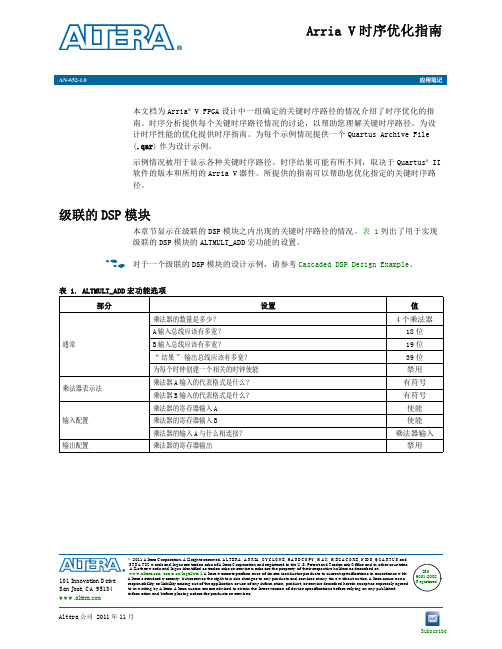
芯片设计中的时钟与时序优化策略在芯片设计的过程中,时钟与时序优化策略起着至关重要的作用。
时钟和时序是芯片设计中的两个关键概念,它们不仅决定了芯片的稳定性和性能,也对整个芯片系统的功能实现起到了至关重要的影响。
本文将介绍时钟与时序的概念,并详细探讨芯片设计中的时钟与时序优化策略。
一、时钟的作用和优化策略时钟是芯片设计中的重要组成部分,它负责驱动芯片内各个模块的工作。
时钟信号的频率和稳定性直接影响到芯片的性能和功耗。
为了优化时钟的作用,芯片设计者可以采取以下策略:1. 时钟频率优化:在芯片设计的过程中,可以通过分析芯片的工作负载和需求,合理地选择时钟频率。
高频率的时钟信号可以提高芯片的性能,但也会增加功耗和热量。
因此,需要在性能和功耗之间寻找一个平衡点,选择适当的时钟频率。
2. 时钟分配优化:对于大型芯片来说,时钟信号需要被准确地传递给各个模块。
合理的时钟分配可以减少时钟信号路径的长度,并降低时钟信号的延迟和损耗。
通过优化时钟布线和时钟网络的结构,可以提高芯片的运行稳定性和性能。
3. 时钟电源噪声优化:时钟信号与电源噪声之间存在着较大的相关性。
电源噪声会影响时钟信号的稳定性和质量,从而对芯片的性能产生不利影响。
因此,在芯片设计中,需要采取相应的措施来降低电源噪声,例如使用合适的电源滤波器和电源隔离技术。
二、时序的作用和优化策略时序是指芯片内各个时钟驱动模块工作时间的先后顺序。
时序设计的好坏对芯片的正常运行和性能有着至关重要的影响。
以下是一些时序优化策略的简要介绍:1. 时序约束优化:在芯片设计的过程中,需要对时序进行约束,以确保芯片的各个模块能够在正确的时间完成相应的操作。
通过细致的时序约束优化,可以最大程度地减少时序故障和互连延迟,提高芯片的工作效率和稳定性。
2. 时序路径优化:时序路径是指数据信号从输入端到输出端所经过的逻辑路径。
时序路径的优化可以通过合理的电路设计和时钟分配来实现。
通过减少时序路径的长度和延迟,可以降低芯片的功耗和时序故障率,提高芯片的性能和可靠性。
Quartus II Software Design Series : Optimization Optimization Techniques –Timing Optimization© 2009 Altera CorporationTiming Optimizationn General Recommendationsn Analyzing Timing Failuresn Solving Typical Timing Failures© 2009 Altera CorporationGeneral Recommendationsn Clocksn I/On Asynchronous Control Signalsn Many of these suggestions are found in Timing Optimization Advisor & Quartus II Handbook© 2009 Altera CorporationClocksn Optimize for Speed-Apply globally-Apply hierarchically-Apply to specific clock domainn Enable netlist optimizations n Enable physical synthesis© 2009 Altera CorporationGlobal Speed Optimizationn Select speed-Default is balanced-Area-optimized designs may also show speed improvements n May result in increased logic resource usage© 2009 Altera CorporationIndividual Optimizationn Optimization Technique logic option -Use Assignment Editor or Tcl to apply to hierarchical block n Speed Optimization Technique for Clock Domains logic option-Use Assignment Editor or Tcl to apply to clock domain or between clock domains© 2009 Altera CorporationSynthesis Netlist OptimizationsnFurther optimize netlists during synthesis n Types-WYSIWYG primitive resynthesis-Gate-level register retimingCreated/modified nodesnoted in Compilation Report© 2009 Altera CorporationWYSIWYG Primitive Resynthesis n Unmaps 3rd-party atomnetlist back to gates &then remaps to Alteraprimitives-Not intended for use withintegrated synthesisn Considerations-Node names may change-3rd-party synthesis attributesmay be lostl Preserve/keep-Some registers may besynthesized away© 2009 Altera CorporationGate-Level Register Retimingn Moves registers across combinatorial logic to balance timingn Trades between critical & non-critical pathsn Makes changes at gate level© 2009 Altera CorporationPhysical Synthesisn Re-synthesisbased on fitteroutput-Makesincrementalchanges thatimprove resultsfor a givenplacement-Compensates forrouting delaysfrom fitter© 2009 Altera CorporationPhysical Synthesisn Types-Targeting performance:l Combinational logicl Asynchronous signal pipeliningl Register duplicationl Register retiming-Targeting fittingl Physical synthesis for combinatorial logicl Logic to memory mappingn Effort-Trades performance vs. compile time-Normal, extra or fastn New or modified nodes appear in Compilation Report© 2009 Altera CorporationCombinational LogicnSwaps look-up table (LUT) ports within LEs to reduce critical path LEsf gab -criticalc d ef ga e c d b© 2009 Altera CorporationAsynchronous Control Signalsn Improve Recovery & Removal Timingn Make control signal non-global-Project-widel Assignments ÞSettings ÞFitter Settings ÞMore Settings -Individuallyl Set Global Signal logic option to Offn Enable “Automatic asynchronous signal pipelining” option (physical synthesis)© 2009 Altera CorporationAsynchronous Signal PipeliningnAdds pipeline registers to asynchronous clear or load signals in very fast clock domainsaclraclrD Q aclraclr D QDQD QaclraclraclrAdded pipeline stageGlobal clock delay© 2009 Altera CorporationDuplicationn High fan-out registers or combinatorial logic duplicated & placed to reduce delayN© 2009 Altera CorporationRegister Retimingn Uses fewer registers than pipelining-Trade off the delay between timing-critical and non-critical paths -Reduce switching-Does not change logic functionalityD Q10 ns D QD Q 5 nsD Q7 ns D QD Q8 ns© 2009 Altera CorporationTiming Optimizationn General Recommendationsn Analyzing Timing Failuresn Solving Typical Timing Failures© 2009 Altera CorporationAnalyzing Timing FailuresnTypical synchronous path-Registers can be internal or external to FPGAREG1REG2Input Failure External Internal Output Failure Internal External Failure within Clock DomainInternalInternal© 2009 Altera CorporationSlack Equations Setup Slack Equation:(latch edge + T clk2 –T su ) –(launch edge + T clk1+ T co + T data )Hold Slack Equation:(launch edge + T clk1+ T co + T data ) –(latch edge + T clk2 + T h )Data ArrivalData RequiredT su , T h , T co are usually fixed values; Function of siliconData ArrivalData Required© 2009 Altera CorporationSlack Equations (cont.)Setup Slack Equation:(latch edge + T clk2 –T su ) –(launch edge + T clk1+ T co + T data )Hold Slack Equation:(launch edge + T clk1+ T co + T data ) –(latch edge + T clk2 + T h )Data ArrivalData RequiredData ArrivalData RequiredTiming issues show up here© 2009 Altera CorporationTypical Timing Errors n Clock delays (T clk1 or T clk2)-Ripple/gated clocks-Non-global routingn Data path delay (T data ) -Fan-out-Too many logic levels-Poor placement-Physical limitations© 2009 Altera CorporationExploring Failures in Quartus II Softwaren Technology Map Viewer-Graphically shows number of logic levelsn Chip Planner-Graphically shows placementn TimeQuest path analysis-Highlights clock/path delays-Highlights fan-out-Highlights number of logic levels-And just about everything else© 2009 Altera CorporationTechnology Map ViewernAccessing Technology Map Viewer -Right-click in TimeQuest report and choose Locate Path or Locate Endpoints nView number of logic levels in failing paths© 2009 Altera CorporationChip PlannerChoose Chip Plannerand the Chip Plannerdisplays the placement,routing & timinginformation for that pathn Accessing Chip Planner-Right-click in TimeQuest report and choose Locate Path or Locate Endpoints n View placement of nodes in timing path as well as chosen routing© 2009 Altera CorporationTimeQuest Path AnalysisLogic Delay Path DelaysInterconnect Delay ClockDelayn Provides ALL detailed information pertaining to timing path© 2009 Altera CorporationFurther Path Analysisn Always start with worst slack path(s)-Fixing worst path(s) may give Fitter freedom to fix other failing pathsn In TimeQuest reports, list top 50-100 failing paths and look for common source, intermediate or destination nodes-Sometimes start or end nodes are bits of same bus-Sometimes paths with different source or destination nodes have common intermediate nodes© 2009 Altera CorporationTiming Optimizationn General Recommendationsn Analyzing Timing Failuresn Solving Typical Timing Failures© 2009 Altera CorporationSolving Typical Timing FailuresWe’ll look at some cases of timing failures, how to identify them and possible solutions. It is possible for you to have several at once.1)Too many logic levels2)Fan-out signals3)Conflicting physical constraints4)Conflicting timing assignments5)Tight timing requirements© 2009 Altera CorporationCase 1) Too Many Logic Levelsn Increases T data, thus increasing data arrival time n How to verify-Technology Map Viewer on failing path-TimeQuest detailed path analysis© 2009 Altera CorporationCase 1) Technology Map ViewerRight-click on failing path and select Locate Endpoints or PathThis path has 8 levels of logic© 2009 Altera CorporationCase 1) TimeQuestNote number oflevels of logic in data arrival path© 2009 Altera CorporationCase 1) Possible Solutionsn Add multi-cycle assignments if design allows n Add pipeline registers-Reduces logic levels-Adds latencyn Enable register retiming (physical synthesis) -Redistributes logic around registers reducing number of levels-Increases compile timen Recode logic to be more efficient-Reduces logic levels-May need to focus on implementation Changes Launch & Latch EdgesChanges Tdata Changes T dataChanges Tdata© 2009 Altera CorporationCase 1) Pipeline Registersn Add pipeline registers to reduce Tdata© 2009 Altera CorporationCase 1) Focus on Implementation n HDL coding decisions will greatly impact resulting synthesis-May need to code with resulting synthesis in mindn See Quartus II handbook chapter, “Recommended HDL Coding Styles”n Great material on HDL coding© 2009 Altera CorporationTip #1 -Reduce Embedded IFs n Don’t embed IF statements-Use CASE statements insteadVHDLVerilog© 2009 Altera CorporationTip #1 -Reduce Embedded IFs (cont.)nResulting hardware interpretation© 2009 Altera CorporationTip #2 -Use System Verilog Unique Casen Verilog CASE implies one-to-many relationshipn Verilog CASE statement is implemented as a priority encoderi.e. embedded IF statementsn System Verilog is a superset of Verilogn Use “unique” qualifier to prevent priority encoder© 2009 Altera CorporationUnique and Priorityn unique and priority keywords apply to case statements or if/else chainsn unique implies non-overlapping case items or conditional expressionsn priority implies just the oppositeunique case(state)S0:S1:S2:endcaseNo more parallel_case!© 2009 Altera CorporationEnabling SystemVerilog-2005 n GUIn Source-level control (for IP etc) n Per-file basis Verilog-2001remains the default// synthesis VERILOG_INPUT_VERSION SYSTEMVERILOG_2005module(input byte a, b, output logic);set_global_assignment –name VERILOG_FILE –rev SYSTEMVERILOG_2005© 2009 Altera CorporationTip #3: CASE synthesis directivesn Don’t use synthesis directives -parallel_case-full_casen Great paper discusses the perils of CASE synthesis directives-"full_case parallel_case",the Evil Twins of Verilog Synthesisl(http://www.sunburst-/papers/CummingsSNUG1999Boston_FullParallelCase.pdf)© 2009 Altera CorporationCase 2) Fan-Out Signalsn Timing failures from fan-out are more often a matter of where than of how many-High fan-out in itself can force nodes to spread out or can result in slow routingl Increases routing delay and thus T datal Proximity is key in FPGAs & newer CPLDsn Typical problem cases:-Memory control signals-Clock enables© 2009 Altera CorporationCase 2) Fan-Out Signals (cont.)n How to verify-Locate high fan-out signals as possible causesl TimeQuest path analysisl Non-Global High Fan-Out Signals table in Compilation Report (Fitterfolder ÞResource section)-Use Chip Planner to verify locations of nodes© 2009 Altera CorporationCase 2) TimequestFanout of 4108 with interconnect delay of 4.429 ns InterconnectDelay© 2009 Altera CorporationCase 2) Possible Solutionsn Add multi-cycle assignments if design allowsn Put high fan-out signals on globals -Reduces delays-Subject to resource availability-Global insertion delay may make thisoption not validn Turn on physical synthesis-Duplicates logic to reduce fan-out-Longer compilation time & higher utilization Changes Launch & Latch EdgesChanges TdataChanges Tdata© 2009 Altera CorporationCase 2) Possible Solutions (cont.) n Use max_fanout constraints -Simple to do-Trial & error process, multiplecompilesn Manual duplication of logic-Reduces fan-out-Allows user to intelligently controlhow each copy is used in design-May be a time intensive process depending on how signal is distributed Changes Tdata Changes Tdata© 2009 Altera Corporationn Examine Fitter report for global & non-global signalsn Fixed number of global signals in a given devicen Fitter algorithms may auto-promote high fan-out signals (see fitter messages)© 2009 Altera Corporationn Manually promote signals with global assignmentn Thru TCL interfaceset_instance_assignment -name GLOBAL_SIGNAL ON -to inst1nThru GUI© 2009 Altera CorporationCase 2) Physical Synthesisn Options to try-Combinational physical synthesisl Performs duplication for combinatorial nodes -Register duplicationn See Quartus II handbook chapter “Netlist Optimizations & Physical Synthesis”-Explains features in detail-Lists caveats and exceptions© 2009 Altera CorporationCase 2) MAX_FANOUT Constraintn Controls the number of destinations so the fan-out count does not exceed the value specifiedn Thru TCL interfaceset_instance_assignment -name MAX_FANOUT <integer>-to <instance>nThru GUI© 2009 Altera CorporationCase 2) Manual Duplication n Two methods:1.Manual duplication in source code 2.Manual Logic Duplication assignmentnManual Logic Duplication Assignment -Duplicates the source node, and uses the new duplicated node to fanout to the destination node。
时序约束当程序编译出现时序问题,并且影响具体功能实现时采取更强的时序约束,如下图所示:具体解决方式是进行时序约束,以调整时序。
具体操作步骤如下:1.右击TimeQuest Timing Analyzer选择open。
打开TimeQuest Timing Analyzer如下图所示。
右击Create Timing Netlist,生成网表如下图所示。
2.生成网表后进行时序约束。
在TimeQuest Timing Analyzer菜单栏下选择constraints下的Create Clock。
依次进行时钟设置,Targets需要进行选择。
设置完毕如下图,点击Run设置完毕。
在次选择TimeQuest Timing Analyzer菜单栏下选择constraints下的Create Generated Clock,对约束时钟进行设置。
设置完毕点击Run。
3.运行完毕后右击Write SDC File选择Start,如下图将文件保存为comLogic.out。
扩展名为.sdc的文件。
4.将3步骤中产生的文件加入工程,重新编译。
编译结果如下图,可以看到红色文字全部消失。
则时序约束完成。
5.但是在实际应用过程中此时有可能在Fast 1200mV 0C Model的HoldSummary仍然出现问题(本次结果没有出现问题)如下图所示:此时需要将主菜单下的Assignments的setting进行设置。
由于芯片工艺等问题需要更强的约束,如图所示需要将Fitter Setting中的Optimize multi-corner timing勾选上等操作。
这样简单的时序约束就可以完成。