(完整word版)Universal Bridge模块
- 格式:doc
- 大小:236.51 KB
- 文档页数:8

实验一-单相桥式全控整流电路实验一单相桥式全控整流电路姓名:王栋班级:15级自动化(2)班学号:1520301081一、实验目的1.加深理解单相桥式全控整流电路的工作原理2.研究单相桥式变流电路整流的全过程3.掌握单相桥式全控整流电路MATLAB的仿真方法,会设置各模块的参数。
二、预习内容要点1. 单相桥式全控整流带电阻性负载的运行情况2. 单相桥式全控整流带阻感性负载的运行情况3. 单相桥式全控整流带具有反电动势负载的运行情况三、实验仿真模型图 1.1 单相桥式阻性负载整流电路四、实验内容及步骤1.对单相桥式全控整流带电阻性负载的运行情况进行仿真并记录分析改变脉冲延迟角时的波形(至少3组)。
以延迟角30°为例(1)器件的查找以下器件均是在MATLAB R2017b环境下查找的,其他版本类似。
有些常用的器件比如示波器、脉冲信号等可以在库下的Sinks、Sources 中查找;其他一些器件可以搜索查找(2)连接说明有时查找出来的器件属性并不是我们想要的例如:变压器可以双击变压器进入属性后,取消three windings transformer就是单相变压器。
(3)参数设置1.双击交流电源把电压设置为311V,频率为50Hz;2.双击脉冲把周期设为0.02s,占空比设为10%,延迟角设为30度,由于属性里的单位为秒,故把其转换为秒即,30×0.02/360;3.双击负载把电阻设为1Ω;4.双击示波器把Number of axes设为7;5.在“Power Electronics”库中选择‘Universal Bridge’模块,选择桥臂数为2,器件为晶闸管,晶闸管参数保持默认即可(4)仿真波形及分析当α=30°时,当α=60°时,当α=90°时,2. 对单相桥式全控整流带阻感性负载的运行情况进行仿真并记录分析改变脉冲延迟角时的波形(至少3组)。
将阻性负载改为阻感负载,即参数设置,双击负载把电阻设为1Ω,电感设为0.01H仿真波形及分析当α=30°时,电感设为0.01H,此时电流处于连续状态图:阻感负载且电流连续时波形将电感值改为0.001H,可以看到电流不连续时的波形如下:图:阻感负载且电流不连续时波形当α=60°时,电感设为0.01H,此时电流处于连续状态将电感值改为0.001H,可以看到电流不连续时的波形如下:当α=90°时,电感设为0.01H,此时电流处于连续状态将电感值改为0.001H,可以看到电流不连续时的波形如下:3. 对单相桥式全控整流带具有反电动势负载的运行情况进行仿真并记录分析改变脉冲延迟角时的波形(至少3组)。
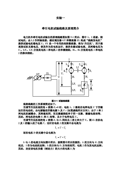
实验一牵引电机试验线路及原理简介电力机车牵引电机试验台的原理线路图如图5-1所示:图中1、2是被、陪试电机,由LJ 作同轴连接。
感应调压器GT 和整流器ZL 构成“线路发电机”提供试验电机端电压U ;SY 是一个专用的相控整流器,称为“升压机”,用于提高陪试机支路电压,使其作为发电机运行,提供负载试验电流,其两端电压为U s 。
LF 1、LF 2分别是电机1和电机2的串激绕组;H 1、H 2分别是电机1和电机2的换向绕组。
图5-1 试验线路图 现将线路的工作原理简述如下:当调节升压机相控角α使得E s =0时,电机1、2都是在电网电压U 下空载运行的电动机,由电源输送空载电源I 0及I '0(如图虚线所示方向),由于1和2两电机机械耦合,其转速相同,而且激磁绕组串于同一支路,激磁电流相等,因此,两电机的电势E 1和E 2相等,且小于电网电压U 。
当调节升压机相控角α使得E s 与E 2同向且二者之和大于U ,则Es 在机电2及1的输入送了电流I',这时在电机2的支路中总电流为2I I I '-'= 而在电机D 的支路中总电流为1I I I '+'= I 1与I 2的电流方向如图中所示,按照图中所示的极性,I 1的方向与E 1方向相反,1作为电动机运转;I 2的方向与E 2方向相相同,电机2作为发电机运转。
因此,决定该电机负载(制动力)的大小的电流I 2为()222R UE E I S -+=式中,R 2为电机2的电枢、换向极及补偿绕组的电阻。
如上所述,此线路的升压机SY 的作用可归结为:如没有升压机,则作为负载电机(陪试机)的电机2就不可能作为发电机运转。
当升压机E S 过低时,可能使E S +E 2≤U ,这时电机1与2就是处于空载状态下的串激电动机,它们将处于飞速状态,因此,在试验过程中,过分调大升压机的相控角α是不允许的。
试验起动过程是:先调高线路机输出电压(不超过试验电机的30%),使机组成并联电动机运行,然后调节升压机增加负载电流,再调节线路机电压、再调节升压机调整负载电流,直到需要的试验值为止。

附件1:学号:27基础强化训练单相交直交变频电路性能研题目究学院自动化学院专业班级姓名指导教师2012年7月10日1 总体原理图 (4)1.1方框图 (4)1.2电路原理图 (4)1.2.1 主回路电路原理图 (4)1.2.2 整流电路 (5)1.2.3 滤波电路 (6)1.2.4 逆变电路 (6)2 电路组成 (9)2.1控制电路 (9)2.2驱动电路 (10)2.3主电路 (11)3 仿真结果 (12)3.1仿真环境 (12)3.2仿真模型使用模块提取的路径与其单数设置 (12)3.3具体仿真结果 (16)3.3.1仿真电路图 (16)3.3.2整流滤波输出电压计算与仿真 (17)3.3.3逆变输出电压计算与仿真 (18)4 小结心得 (20)5 参考文献 (21)基础强化训练任务书学生姓名:专业班级:指导教师:工作单位:题目: 单相交直交变频电路性能研究初始条件:输入为单相交流电源,有效值220V。
要求完成的主要任务:(1)掌握单相交直交变频电路的原理;(2)设计出系统结构图,并采用matlab对单相交流调压电路进行仿真;(3)采用protel设计出单相交直交变频电路主电路、驱动电路、控制电路时间安排:2012年7月9日至2012年7月13日,历时一周,具体进度安排见下表参考文献:[1]王兆安,刘进军.《电力电子技术》第5版.北京:机械工业出版社,2011指导教师签名: 年 月 日 系主任(或责任教师)签名: 年 月 日 1 总体原理图1.1 方框图图1 总体方框图1.2 电路原理图1.2.1 主回路电路原理图图2 主回路原理图如图所示,交直流变换电路为不可控整流电路,输入的交流电通过变压器和桥式整流电路转化为直流电,滤波电路用电感和电容滤波,逆变部分采用四只IGBT管组成单项桥式逆变电路,采用双极性调制方式,输出经LC低通滤波器滤波,滤除高次谐波,得到频率可调的交流电输出。
1.2.2 整流电路整流电路的功能是把交流电源转换成直流电源。

matlab中universal bridge模块的用法-回复Matlab是一种常用的科学计算软件和编程环境,提供了许多丰富的模块和工具包来支持各种计算任务。
其中,Universal Bridge(通用桥接)模块是一个非常有用的工具,可以帮助用户在Matlab中连接不同的编程语言和软件包,以实现各种复杂的计算任务。
本文将介绍Universal Bridge模块的详细用法,帮助读者理解如何使用该模块。
第一步:安装Universal Bridge模块在开始使用Universal Bridge模块之前,我们首先需要安装该模块。
通常,Matlab会自带一些常用的模块和工具包,但对于一些特定的模块,可能需要手动安装。
要安装Universal Bridge模块,我们可以按照以下步骤进行操作:1. 在Matlab界面的菜单栏中选择"Home"。
2. 在打开的菜单中,选择"Add-Ons"。
3. 在Add-Ons界面,可以看到所有可用的模块和工具包。
在搜索框中输入"Universal Bridge",找到对应的模块。
4. 单击"Install"按钮,开始安装Universal Bridge模块。
第二步:连接不同的编程语言和软件包安装完Universal Bridge模块后,我们可以开始连接不同的编程语言和软件包。
Universal Bridge模块支持许多常见的编程语言和软件包,例如C/C++、Python、Java、R等。
假设我们要连接Python和Matlab,以实现一些Python中已有的函数或算法在Matlab中的调用。
以下是连接Python的示例代码:matlab首先,加载Universal Bridge模块universallib('load', 'python');接下来,创建一个Python桥接对象,并指定Python解释器的路径py = universallib('python');universallib('set', py, 'Interpreter', 'path_to_python_interpreter');然后,我们可以使用Python桥接对象来调用Python中的函数或算法result = universallib('call', py, 'python_function_name', arg1,arg2, ...);最后,关闭Python桥接对象universallib('destroy', py);在上述代码中,我们首先加载Universal Bridge模块,并创建一个Python桥接对象。

simulink中universal bridge模块使用方法Simulink中的Universal Bridge模块是一个非常有用的模块,它允许您模拟不同类型的桥梁结构,例如悬索桥、拱桥、梁桥等。
下面是Universal Bridge模块的一些使用方法:1. 打开Simulink模型:在MATLAB命令窗口中输入“simulink”,然后按Enter 键打开Simulink库浏览器。
2. 创建新模型:在Simulink库浏览器中,单击“File”菜单,然后选择“New”>“Model”。
3. 添加Universal Bridge模块:在Simulink库浏览器中,展开“Simulink”>“Sinks”>“Universal Bridge”文件夹,然后单击“Universal Bridge”模块并将其拖放到模型中。
4. 配置Universal Bridge模块:双击Universal Bridge模块,将出现一个配置对话框。
您可以在其中设置以下参数:* “Bridge Type”:选择桥梁类型,例如悬索桥、拱桥、梁桥等。
* “Number of Girders”:设置桥面数量。
* “Girders Spaced By”:设置桥面之间的距离。
* “Girders Parallel”:设置桥面是否平行。
* “Top Girders Fixed”:设置顶部桥面是否固定。
* “Bottom Girders Fixed”:设置底部桥面是否固定。
* “Bridge Material”:设置桥梁材料,例如钢、混凝土等。
* “Bridge Cross-Sectional Area”:设置桥梁横截面积。
* “Bridge Weight”:设置桥梁重量。
5. 连接其他模块:使用信号线将其他模块连接到Universal Bridge模块上,以便模拟桥梁的加载和响应。
6. 运行仿真:单击Simulink工具栏中的“Run”按钮,开始仿真模拟。

Clover 设置新手教程1.Clover的Config。
plist是基于XML编写的,可以看成一个文本文档,Windows下使用Notepad ++ 或者使用写字板编辑;Mac 下使用PlistEdit Pr o2。
Config。
plist必须放置于 /EFI/Clover 文件夹下3。
一些基本的设定规则:(1)如果你不知道这个参数是干什么的,或者他的值应该是多少,那么直接从config里删除掉这个参数。
(2)不要设定你不知道的参数以及参数所对应的值。
(3)任何参数都需要一个值,宁可删掉这个参数,也不要留空不填(不填写这个参数的值)。
4。
在Clover引导界面,进入Option设置,可以方便地临时修改各个参数的设定在引导系统安装时,config.plist的参数尽可能从简Boot 模块一些杂项设置Arguments 选项〈key>Arguments〈/key〉<string〉ARGUMENTS〈/string〉在这部分,你可以添加”Boot Flags" 启动项参数和 "Kernel Flags" 内核项参数,来由系统调用使用。
这些参数源自chameleon(变色龙),主要起到解决系统不正常引导和启动及一些功能上修复作用。
具体参数详解如下:”Boot Flags”启动项参数<key〉Arguments〈/key><string>—v –s –x〈/string>-v 啰嗦模式启动:不能正常进入系统时采用,故障调试,显示所有调试日志(含错误信息)-s 启动 OS X 进入单用户模式:不能正常进入系统时采用,脱离图形界面,以命令行方式进入,不适合新手适用。
-x 启动 OS X 进入 SafeBoot(安全模式):不能正常进入系统时采用.其他启动项参数调用详见>>专贴"Kernel Flags"内核项参数arch参数〈key〉Arguments</key〉<string>arch=i386 arch=x86_64</string〉参数说明:arch=i386/x86_64两个参数不能同时启用。
用MATLAB 仿真一个单相全桥逆变器,采用单极性SPWM 调制、双极性SPWM 调制或者单极倍频SPWM 调制的任意一种即可,请注明仿真参数,并给出相应的调制波波形,载波波形,驱动信号波形、输出电压(滤波前)波形。
本文选用双极性SPWM 调制。
1双极性单相SPWM 原理SPWM 采用的调制波的频率为s f 的正弦波t U U s sm S ωsin =,s s f πω2=;载波c u 就是幅值为cm U ,频率为c f 的三角波。
载波信号的频率与调制波信号的频率之比称为载波比,正弦调制信号与三角波调制信号的幅值之比称为深度m 。
通常采用调制信号与载波信号相比较的方法生成SPWM 信号、当Us>Uc 时,输出电压Uo 等于Ud,当Us<Uc 时,输出信号Uo 等于-Ud 、随着开关以载波频率fc 轮番导通,逆变器输出电压不断在正负Ud 之间来回切换。
2 建立仿真模型2、1主电路模型第一步设置电压源:在Electrical Sources 库中选用DC Voltage Source,设置Ud =300V 。
第二步搭建全桥电路:使用Universal Bridge 模块,选择桥臂数为2,开关器件选带反并联二极管的IGBT/Diodes,构成单项全桥电路。
第三步使用Series RLC Branch 设置阻感负载为1Ω,2mH,并在Measurement 选项中选择Branch Voltage and current,利用multimeter 模块观察逆变器的输出电压与电流。
电路如图2、1所示。
图2、1 单相全桥逆变逆变器电路图2、2双极性SPWM信号发生器在Simulink的Source库中选择Clock模块,提供仿真时间t,乘以fπ2后通过一个sin模块即tωsin,乘以调整深度m可获得所需的正弦调整信号。
选择Source库中的Repeating Sequence模块产生三角载波,设置Time Values 为[0 1/fc/4 3/fc/4 1/fc],设置Output Values 为[0 -1 1 0],生成频率为fc的三角载波。
三相桥式全控整流电路的M a t l a b仿真及其故障分析三相桥式全控整流电路的MATLAB仿真及其故障分析摘要:设计一种以三相桥式全控整流电路的MATLAB仿真及其故障分析。
以三相桥式全控整流电路为分析对象,利用Matlab/Simulink环境下的SimPowerSystems仿真采集功率器件在开路时的各种波形,根据输出波形分析整流器件发生故障的种类,判断故障发生类型,确定发生故障的晶闸管,实现进一步故障诊断。
运用matlab中的电气系统库可以快速完成对三相整流电路故障仿真,通过分析可以对故障类型给予初步判断,对电力电子设备的开发、运用以及维修有极大的现实意义。
关键词:Matlab;三相整流桥;电力电子故障Matlab Simulation and Trouble Analysis of the Three-Phase Full-Bridge Controlled RectifierZhang lu-xiaCollege of Physics& Electronic Information Electrical Engineering &Automation No: 060544076Tutor: Wu yanAbstract: the article introduces a design of Matlab Simulation and Trouble Analysis of the Three-Phase Full-Bridge Controlled Rectifier. using the three-phase full-bridge controlled rectifier circuit for analysis, the output waveform in each kind of fault can be simulated through the circuit with the SimPower Systems under the Matlab/Simulink surroundings, for sure the SCR of having troubles in order to fulfill further trouble diagnoses. it can finish Matlab Simulation ahout electrical system1quickly and fulfill further trouble diagnoses. it will play an important role in the field of electric power & electron on equipment exploration and maintenance..key words: Matlab; three-phase rectifier bridge; power electronics trouble目录1 引言 (3)2 三相全控整流电路 (4)2.1 整流器件 (4)2.2 整流原理 (4)2.2.1 触发脉冲 (5)2.2.2 带电阻负载时的工作情况 (6)2.2.3 带阻感负载时的工作情况 (8)3 三相桥式全控整流电路仿真建模 (10)3.1 仿真模块 (10)3.1.1 交流电压源模块 (10)3.1.2 选择开关 (10)3.1.3 晶闸管的仿真模型 (11)3.1.4 同步6脉冲触发器的仿真模型 (12)3.1.5 常数模块参数的设置 (13)3.1.6 通用桥设置 (13)3.1.7 显示模块 (14)3.2 三相全控整流电路的matlab仿真 (14)3.2.1 带电阻负载的仿真 (14)3.2.2 阻感负载的仿真 (16)4 故障分析 (17)5 结束语 (18)1 引言在电力、冶金、交通运输、矿业等行业,电力电子器件通常被用于电机变频调速、大功率设备驱动的关键流程之中,由于电力电子器件故障往往是致命性的、不可恢复的,常导致设备的损毁、生产的中断,造成重大经济损失。
带电容滤波的三相不控整流桥M A T L A B仿真标准化管理部编码-[99968T-6889628-J68568-1689N]计算机仿真技术作业二题目:带电容滤波的三相不控整流桥仿真利用simpowersystems建立三相不控整流桥的仿真模型。
输入三相电压源,线电压380V,50Hz,内阻0.001Ω。
三相二极管整流桥可用“Universal Bridge”模块,二极管采用默认参数。
直流滤波电容3300μF,负载为电阻。
仿真时间0.3s。
注:前三项只考虑稳态情况,第四项注重启动过程。
建立系统仿真模型如下图:仿真算法选择ode23tb,最大步长为1μs,仿真时间0.3s理论计算:当二极管用理想开关代替,直流侧空载时,输出直流电压与输入交流线电压的关系如下:交流侧电流有效值:交流侧基波电流有效值:1、直流电压与负载电阻的关系:分别仿真整流电路空载及负载电阻为10、1和0.1欧姆时的情况。
记录直流电压波形,根据仿真结果求出直流电压,并比较分析其与负载的关系。
理论计算(1)空载时直流电压Ud =537.4V ,纹波电压ΔUd=0(2)负载电阻为50Ω时直流电压Ud =533.2V ,纹波电压ΔUd=8.75V(3)负载电阻为10Ω时直流电压Ud =523.3V ,纹波电压ΔUd=32.5000V(4)负载电阻为1Ω时直流电压 Ud =511.1V 纹波电压ΔUd= 70.9100 V(5)负载电阻为0.1Ω时直流电压Ud =493.5V 纹波电压ΔUd= 64.9500 V结论:由以上仿真结果可得到如下结论: 输出直流电压的值随着负载电阻的减小而减小2、电流波形与负载的关系:分别仿真负载电阻为10、1.67和0.5时的情况。
记录直流电流和a相交流电流,并分析规律。
(1)负载电阻为50Ω时,a相交流电流和直流电流波形如下图:(1)负载电阻为10Ω时,a相交流电流和直流电流波形如下图:(2)负载电阻为1.67Ω时,a相交流电流和直流电流波形如下图(3)负载电阻为0.5Ω时,a相交流电流和直流电流波形如下图结论: 由以上仿真结果可得到以下结论,随着负载电阻的减小,直流侧电流Id ,交流侧电流Ia逐渐增大,直流侧电流有效值和交流侧电流有效值具有如下的近似关系:当负载电阻为1.67Ω时,输出电压为Vd=512v,与理论计算接近。
《功率电子学课程设计》设计报告设计时间:2012.06.05班级:10应用电子及技术(1)班姓名:报告页数:15广东工业大学课程设计报告设计题目晶闸管直流调速系统参数和环节特性的测定实验学院信息工程专业应用电子技术班(1)学号姓名成绩评定_______教师签名_______晶闸管直流调速系统参数和环节特性的测定实验1、实验目的(1)熟悉晶闸管直流调速系统的组成及其基本结构。
(2)掌握晶闸管直流调速系统参数及反馈环节测定方法。
2、实验原理晶闸管直流调速系统由整流变压器、晶闸管整流调速装置、平波电抗器、电动机—发电机住等组成。
在本实验中,整流装置的主电路为三相桥式电路,控制电路可直接由给定电压U g作为触发器的移相控制电压U ct,改变Ug的大小即可改变控制角α,从而获得可调的直流电压,以满足实验要求。
实验系统的组成原理如图1所示。
图1 晶闸管直流调速实验系统原理图3、实验内容(1)测定晶闸管直流调速系统主电路总电阻值R。
(2)测定晶闸管直流调速系统住电感值L。
(3)测定直流电机—直流发电机—测速发电机组的飞轮惯量GD2。
(4)测定晶闸管直流调速系统主电路电磁时间常数T d。
(5)测定直流电动机电势常数C e和转矩常数C M。
(6)测定晶闸管直流调速系统机电时间常数T M。
(7)测定晶闸管出发及整流装置特性U d=ƒ(U ct)。
(8)测定测速发电机特性U TG=ƒ(n)。
4、实验仿真晶闸管直流调速实验系统的原理图如图1所示。
该系统由给定信号、同步脉冲触发器、晶闸管整流桥、平波电抗器、直流电动机等部分组成。
图2是采用面向电气原理图方法构成的晶闸管直流调速系统的仿真模型。
下面介绍各部分建模与常数设置过程。
图2 晶闸管开环直流调速系统的仿真模型4.1系统的建模和模型参数设置系统的建模包括主电路的建模和控制电路的建模两部分。
(1)主电路的建模和参数设置由图2可见,开环直流调速系统的主电路由三相对称交流电压源、晶闸管整流桥、平波电抗器、直流电动机等部分组成。
Universal Bridge -Implement universal power converter with selectable topologies and power electronic devicesLibraryPower ElectronicsDescriptionThe Universal Bridge block implements a universal three-phase power converter that consists of up to six power switches connected in a bridge configuration. The type of power switch and converter configuration are selectable from the dialog box.The Universal Bridge block allows simulation of converters using both naturally commutated (or line-commutated) power electronic devices (diodes or thyristors) and forced-commutated devices (GTO, IGBT, MOSFET).The Universal Bridge block is the basic block for building two-level voltage-sourced converters (VSC).The device numbering is different if the power electronic devices are naturally commutated or forced-commutated. For a naturally commutated three-phase converter (diode and thyristor), numbering follows the natural order of commutation:For the case of a two-phase diode or thyristor bridge, and for any other bridge configuration, the order of commutation is the following:GTO-Diode bridge:IGBT-Diode bridge:MOSFET-Diode and Ideal Switch bridges:Dialog Box and ParametersNumber of bridge armsSet to 1 or 2 to get a single-phase converter (two or four switching devices). Set to 3 to get a three-phase converter connected in Graetz bridge configuration (six switching devices).Snubber resistance RsThe snubber resistance, in ohms (Ω). Set the Snubber resistance R s parameter to inf to eliminate the snubbers from the model.Snubber capacitance CsThe snubber capacitance, in farads (F). Set the Snubber capacitance Cs parameter to 0 to eliminate the snubbers, or to inf to get a resistive snubber.In order to avoid numerical oscillations when your system is discretized, you need to specify Rs and Cs snubber values for diode and thyristor bridges. Forforced-commutated devices (GTO, IGBT, or MOSFET), the bridge operates satisfactorily with purely resistive snubbers as long as firing pulses are sent to switching devices.If firing pulses to forced-commutated devices are blocked, only antiparallel diodes operate, and the bridge operates as a diode rectifier. In this condition appropriate values of Rs and Cs must also be used.When the system is discretized, use the following formulas to compute approximate values of Rs and Cs:wherePn = nominal power of single or three phase converter (V A)Vn = nominal line-to-line AC voltage (Vrms)f = fundamental frequency (Hz)Ts = sample time (s)These Rs and Cs values are derived from the following two criteria:The snubber leakage current at fundamental frequency is less than 0.1% of nominal current when power electronic devices are not conducting.The RC time constant of snubbers is higher than two times the sample time Ts. These Rs and Cs values that guarantee numerical stability of the discretized bridge can be different from actual values used in a physical circuit.Power electronic deviceSelect the type of power electronic device to use in the bridge.When you select Switching-function based VSC, a switching-function voltage source converter type equivalent model is used, where switches are replaced by two voltage sources on the AC side and a current source on the DC side. This model uses the same firing pulses as for other power electronic devices and it correctly represents harmonics normally generated by the bridge.When you select Average-model based VSC, an average-model type of voltage source converter is used to represent the power-electronic switches. Unlike the other power electronic devices, this model uses the reference signals (uref) representing the average voltages generated at the ABC terminals of the bridge. This model does not represent harmonics. It can be used with larger sample times while preserving the average voltage dynamics.See the power_sfavg demo for an example comparing these two models to an Universal Bridge block using IGBT/Diode device.RonInternal resistance of the selected device, in ohms (Ω).LonInternal inductance, in henries (H), for the diode or the thyristor device. When the bridge is discretized, the Lon parameter must be set to zero.Forward voltage VfThis parameter is available only when the selected Power electronic device is Diodes or Thyristors.Forward voltage, in volts (V), across the device when it is conducting.Forward voltages [Device Vf, Diode Vfd]This parameter is available when the selected Power electronic device is GTO/Diodes or IGBT/Diodes.Forward voltages, in volts (V), of the forced-commutated devices (GTO, MOSFET, or IGBT) and of the antiparallel diodes.[Tf (s) Tt (s)]Fall time Tf and tail time Tt, in seconds (s), for the GTO or the IGBT devices. MeasurementsSelect Device voltages to measure the voltages across the six power electronic device terminals.Select Device currents to measure the currents flowing through the six power electronic devices. If antiparallel diodes are used, the measured current is the total current in the forced-commutated device (GTO, MOSFET, or IGBT) and in the antiparallel diode. A positive current therefore indicates a current flowing in the forced-commutated device and a negative current indicates a current flowing in the diode. If snubber devices are defined, the measured currents are the ones flowing through the power electronic devices only.Select UAB UBC UCA UDC voltages to measure the terminal voltages (AC and DC) of the Universal Bridge block.Select All voltages and currents to measure all voltages and currents defined for the Universal Bridge block.Place a Multimeter block in your model to display the selected measurements during the simulation. In the Available Measurements menu of the Multimeter block, theThe gate input for the controlled switch devices. The pulse ordering in the vector of the gate signals corresponds to the switch number indicated in the six circuits shown in the Description section. For the diode and thyristor bridges, the pulse ordering corresponds to the natural order of commutation. For all other forced-commutatedThe power_bridges demo illustrates the use of two Universal Bridge blocks in an ac/dc/ac converter consisting of a rectifier feeding an IGBT inverter through a DC link. The inverter is pulse-width modulated (PWM) to produce a three-phase 50 Hz sinusoidal voltage to the load. In this example the inverter chopping frequency is 2000 Hz.The IGBT inverter is controlled with a PI regulator in order to maintain a 1 pu voltage (380 Vrms, 50 Hz) at the load terminals.A Multimeter block is used to observe commutation of currents between diodes 1 and3 in the diode bridge and between IGBT/Diodes switches 1 and 2 in the IGBT bridge.Start simulation. After a transient period of approximately 40 ms, the system reaches a steady state. Observe voltage waveforms at DC bus, inverter output, and load on Scope1. The harmonics generated by the inverter around multiples of 2 kHz are filtered by the LC filter. As expected the peak value of the load voltage is 537 V (380 V RMS).In steady state the mean value of the modulation index is m = 0.8, and the mean value of the DC voltage is 778 V. The fundamental component of 50 Hz voltage buried in the chopped inverter voltage is thereforeVab = 778 V * 0.612 * 0.80 = 381 V RMSObserve diode currents on trace 1 of Scope2, showing commutation from diode 1 to diode 3. Also observe on trace 2 currents in switches 1 and 2 of the IGBT/Diodebridge (upper and lower switches connected to phase A). These two currents are complementary. A positive current indicates a current flowing in the IGBT, whereas a negative current indicates a current flowing in the antiparallel diode.。