1
+-1.0 Center CFG16
3
PCI Routing
IDSEL 7412 22 21 23
CFG17 page 16 CFG18
ICH7M Functional Strap Definitions
Signal ACZ_SDOUT Usage/When Sampled XOR Chain Entrance/ PCIE Port Config bit1, Rising Edge of PWROK PCIE bit0, Rising Edge of PWROK. Reserved Reserved Reserved Top-Block Swap Override. Rising Edge of PWROK. Comment
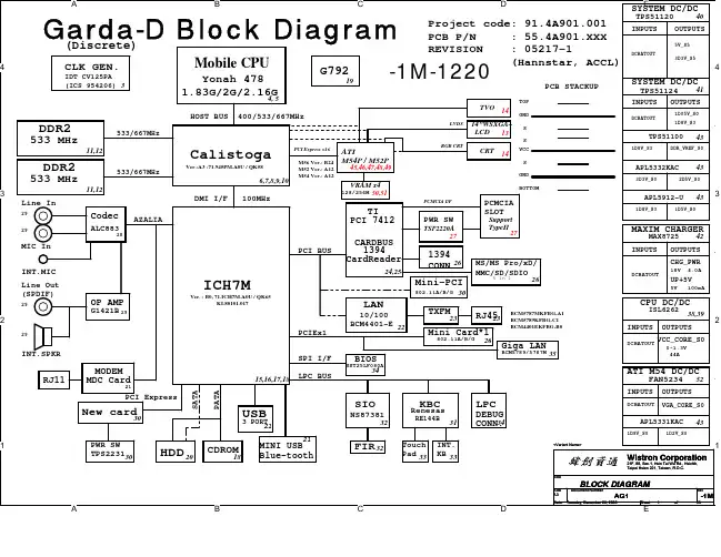
Garda-D Block Diagram (Discrete)
4
A
B
C
D
SYSTEM DC/DC
TPS51120
INPUTS 40 OUTPUTS
5V_S5 DCBATOUT 3D3V_S5
E
CLK GEN.
IDT CV125PA (ICS 954206) 3
Mobile CPU
Yonah 478 1.83G/2G/2.16G 4, 5
EE_DIN, EE_DOUT, GNT[3:0], GPIO[25], GNT[4]#/GPIO48, GNT[5]#/GPO17, PME#,
954305D 27Mhz/LCDCLK Spread and Frequency Selection Table
SS3 Byte9 bit 7 0 0 0 0 0 SS2 bit6 0 0 0 0 1 1 1 1 0 0 0 0 1 1 1 1 SS1 bit5 0 0 1 1 0 0 1 1 0 0 1 1 0 0 1 1 SS0 bit4 0 1 0 1 0 1 0 1 0 1 0 1 0 1 0 1 Spread Amount% -0.50 Down -1.00 Down -1.50 Down -2.00 Down -0.75 Down -1.25 Down -1.75 Down page 3