理想的电压反馈型(VFB)运算放大器
- 格式:pdf
- 大小:226.86 KB
- 文档页数:6
理想的电压反馈型(VFB)运算放大器
简介
运算放大器是线性设计的基本构建模块之一。
在经典模式下,运算放大器由
两个输入引脚和一个输出引脚构成,其中一个输入引脚使信号反相,另一个输
入引脚则保持信号的相位。
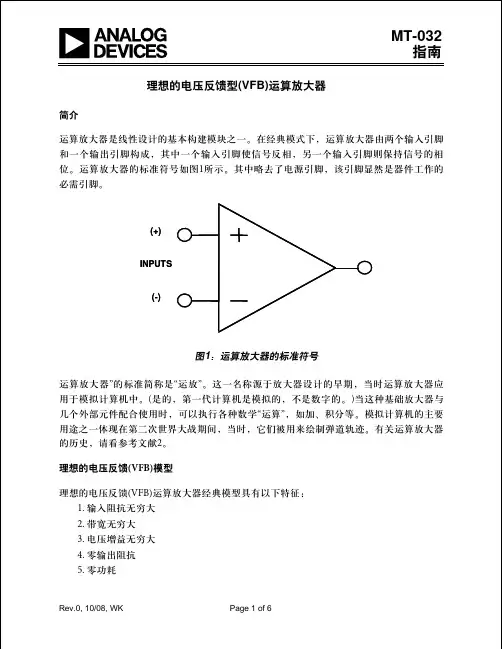
运算放大器的标准符号如图1 所示。
其中略去了电
源引脚,该引脚显然是器件工作的必需引脚。
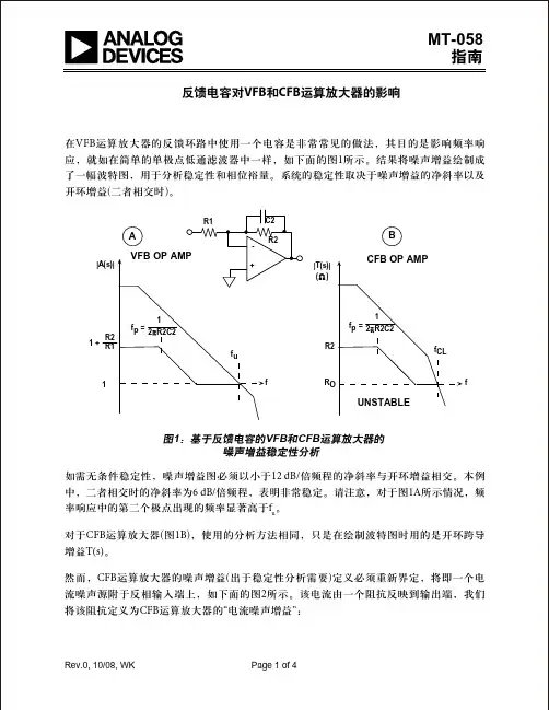
图1:运算放大器的标准符号
运算放大器”的标准简称是”运放”.这一名称源于放大器设计的早期,当时运
算放大器应用于模拟计算机中。
(是的,第一代计算机是模拟的,不是数字的。
)当这种基础放大器与几个外部元件配合使用时,可以执行各种数学”运算”,如加、
积分等。
模拟计算机的主要用途之一体现在第二次世界大战期间,当时,它们
被用来绘制弹道轨迹。
有关运算放大器的历史,请看参考文献2.
理想的电压反馈(VFB)模型
理想的电压反馈(VFB)运算放大器经典模型具有以下特征:
1. 输入阻抗无穷大
2. 带宽无穷大
3. 电压增益无穷大
4. 零输出阻抗
5. 零功耗
虽然这些并不现实,但这些理想标准决定着运算放大器的质量。
这就是所谓的电压反馈(VFB)模型。
这类运算放大器包括带宽在10 MHz 以下的几乎所有运算放大器,以及带宽更高的运算放大器的90%.电流反馈(CFB)是。
理想运算放大器特点
集成运算放大器,简称运放。
三端元件(双端输入、单端输出的电路结构),抱负三极管,高增益直流放大器。
抱负运算放大器(有时简称运放)的特点如下:
(1)极大的输入电阻
高输入阻抗,输入端流入电流近于0,几乎不取用信号源电流,近于电压掌握特性,从而导出“虚断”概念;
(2)微小的输出电阻
具有(在负载力量以内)不挑负载,适应任意负载的特性。
后级负载电路的阻抗大小不会影响到输出电压。
(3)无穷大的电压放大倍数(可达百万或千万倍)。
这就打算了:在肯定供电电压条件下,放大器仅能工作闭环(负反馈)模式下,且实际的放大倍数是有限的;开环模式即为比较器状态,输出为高、低电平二态。
在闭环(有限放大倍数)状态下,放大器的脾性是随机比较两输入端的电位凹凸,不等时输出级即时做出调整动作,放大的最终目的,是使两输入端电位相等(其差为0V),从而导出“虚短”概念。
其实,在放大过程中,是在进行着“放大不离比较,比较不离放大”动态平衡的调整。
整个模拟电路教程,在高校或高职高专的正统教学规程上,其内容相当浩大,而学习难度尤高,尤其牵涉太多的高等数字运算,因而学习
运算电路,被相当多的学子视为畏途,更有人将模拟电路称之为“魔电”,越学越晕,导致不能学以致用。
以我本人几十年来对电子电路的原理把握和实践应用阅历为据,写就该章。
就我看来,整个运放电路的应用,假如用3个课时来解决掉,把握原理和检修方法,一步到位修运放电路,是完全可以实现的。


MT-060TUTORIAL Choosing Between Voltage Feedback (VFB)and Current Feedback (CFB) Op AmpsThe application advantages of current feedback and voltage feedback differ. In many applications, the differences between CFB and VFB are not readily apparent. Many of today's high speed CFB and VFB amplifiers have comparable performance, but there are certain unique advantages and disadvantages associated with each. This tutorial examines some of the important considerations associated with the two topologies.DC AND OPERATIONAL CONSIDERATIONS FOR VFB AND CFB OP AMPSVFB Op Amps•For precision low frequency applications requiring high open-loop gain, low offset voltage, and low bias current, the VFB op amp is the proper choice. Input offset voltages of high speed bipolar input VFB op amps are rarely trimmed, since offset voltage matching of the input stage is excellent, typically ranging from 1 to 3 mV, with offset temperature coefficients of 5 to 15µV/°C. With trimming, input offset voltages of less than 20 µV are achievable. Op amps which use the auto-zero architecture offer offset voltages less than 5 µV, but will not be considered here. The auto-zero op amp is covered in Tutorial MT-055. •Input bias currents on VFB op amps (with no input bias current compensation circuits) are approximately equal for (+) and (–) inputs, and can range from 1 to 5 µA. FET input op amps are available with input bias currents less than 200 fA, suitable for applications such as electrometers. (e.g., AD549).•The output offset voltage due to the input bias currents can be nulled by making the effective source resistance equal in both the inverting and non-inverting inputs. This scheme will not work with bias-current compensated VFB op amps which have additional current generators on their inputs. In this case, the net input bias currents are not necessarily equal or of the same polarity.•The VFB op amp is very useful in applications where the feedback network controls the overall response, such as in active filter applications. Some VFB op amps, however, are de-compensated and must be used above the specified minimum closed-loop gain.•The simplified model for the VFB op amp is well understood and is presented in all analog electronic textbooks.•The VFB architecture lends itself to low supply voltage applications where rail-to-rail inputs and outputs are required.CFB Op Amps•Current feedback (CFB) op amps, on the other hand, are less well understood and documented. Many designers choose VFB op amps simply because they understand them better.•CFB op amps generally have lower open-loop gain and less accuracy than a precision VFB op amp.•The input impedance of the inverting and non-inverting inputs of CFB op amps are not equal, and CFB op amps generally have unequal and uncorrelated input bias currents because the (+) and (–) inputs have completely different architectures. For this reason, external bias current cancellation schemes are also ineffective. CFB input bias currents range from 5 to 15 µA, being generally higher at the inverting input.•Because CFB op amps are geneally optimized for a fixed feedback resistor value, there is little flexibility in the feedback network other than setting the closed-loop gain. This makes CFB op amps unsuitable for most active filters, except for the Sallen-Key filter which can be designed with the appropriate fixed feedback resistor. Figure 1 summarizes the dc and operational considerations for VFB and CFB op amps.•The CFB architecture does lend itself to rail-to-rail inputs and outputs.VFB Op Ampsz High open loop gain and DC accuracyz Low offset voltage available (<20 µV)z Low bias current (JFET, CMOS, or bias current compensation) available (<200 fA)z Balanced input impedancez Flexible feedback networkz Rail-to-rail inputs and outputs availableCFB Op Ampsz Lower open loop gain and DC accuracyz Higher offset voltagez Inverting input impedance is low, non-inverting input impedance is highz Input bias currents not as low as VFB or as well matchedz Fixed feedback resistor needed for optimum performanceFigure 1: DC and Operational Considerations for VFB and CFB Op AmpsAC CONSIDERATIONS FOR VFB AND CFB OP AMPSVFB Op Amps• A distinguishing feature of VFB op amps is that they offer a constant gain-bandwidth product over a wide frequency range.•In addition, high bandwidth, high slew rate, low distortion VFB op amps are available which use the "H-Bridge" architecture for low quiescent current (Tutorial MT-056).•VFB op amps are good for all types of active filter architectures because of the flexibility of the feedback network.CFB Op Amps•The CFB topology is primarily used where the ultimate in high bandwidth high slew rate, and low distortion are required. A more detailed discussion of CFB op amp ac characteristics can be found in Tutorial MT-057.•For a given complementary bipolar IC process, CFB generally yields higher FPBW (hence lower distortion) than VFB for the same amount of quiescent supply current. This is because there is practically no slew-rate limiting in CFB. Because of this, the full power bandwidth and the small signal bandwidth are approximately the same. However, the "H-Bridge"architecture used in high speed VFB op amps almost the same level of performance as CFB op amps (Tutorial MT-056).•Unlike VFB op amps, the inverting input impedance of a CFB op amp is very low. This is advantageous when using the op amp in the inverting mode as an I/V converter, because there is less sensitivity to inverting input capacitance than with VFB.•The closed-loop bandwidth of a CFB op amp is determined by the value of an internal capacitor and the external feedback resistor and is relatively independent of the gain-setting resistor (the resistor from the inverting input to ground). This makes CFB op amps ideal for programmable gain applications which require a gain-independent bandwidth.•Because CFB op amps must operate with a fixed feedback resistor for optimum stability, they have limited applications as active filters, other than the Sallen-Key filter.•Small values of stray capacitance across the feedback resistor in a CFB op amp are likely to cause instability.VFB Op Ampsz Constant gain-bandwidth productz High slew rate and high bandwidth availablez Low distortion versions availablez Flexible feedback networkz Good for active filtersCFB Op Ampsz Bandwidth relatively constant for various closed-loop gainsz Gain-bandwidth product is not constantz Slightly higher slew rate and bandwidth available for givenprocess and power dissipation (compared to VFB)z Low distortion versions availablez Fixed feedback resistor for optimum performancez Stray feedback capacitance causes instabilityz Difficult to use in active filters other than Sallen-Keyz Low inverting input impedance reduces effects of inputcapacitance in I/V converter applicationsFigure 2: AC Considerations for VFB and CFB Op AmpsNOISE CONSIDERATIONS FOR VFB AND CFB OP AMPSVFB Op Amps•Precision VFB op amps are available with input voltage noise less than 1 nV/√Hz. Most JFET or CMOS input VFB op amps have input current noise less than 100 fA/√Hz, with some less than 1 fA/√Hz. However, the total output noise depends not only on these values but the closed-loop gain and the actual values of the feedback resistors (Tutorial MT-049). •For a VFB op amp, the inverting and non-inverting input current noise are typically equal, and almost always uncorrelated. Typical values for wideband bipolar VFB op amps range from 0.5 pA/√Hz to 5 pA/√Hz. The input current noise of a bipolar input stage is increased when input bias-current compensation generators are added, because their current noise is not correlated, and therefore adds (in an rss manner) to the intrinsic current noise of the bipolar stage. However, bias current compensation is rarely used in high speed op amps.CFB Op Amps•The input voltage noise in CFB op amps tends to be lower than for VFB op amps having the same approximate bandwidth. This is because the input stage in a CFB op amp is usually operated at a higher current, thereby reducing the emitter resistance and hence the voltage noise. Typical values for CFB op amps range from about 1 to 5 nV/√Hz.•However, the input current noise of CFB op amps tends to be larger than for VFB op amps because of the generally higher bias current levels. The inverting and non-inverting current noise of a CFB op amp is usually different because of the unique input architecture, and are specified separately. In most cases, the inverting input current noise is the larger of the two.Typical input current noise for CFB op amps ranges from 5 to 40 pA/√Hz. This can often be dominant, except in cases of very high closed-loop gain where the voltage noise can become dominant.The best way to make the noise calculations is to write a simple computer spreadsheet program that performs the calculations automatically, and include all the noise sources. The equation discussed in Tutorial MT-049 can be used for this purpose.VFB Op Ampsz Low voltage noise ( < 1 nV/√Hz) availablez Low current noise available (JFET and CMOS inputs)z Inverting and non-inverting input current noise equal and uncorrelatedz Feedback network and external resistor values must be considered to determine total noiseCFB Op Ampsz Low voltage noise (1 to 5 nV/√Hz)z Higher current noise (5 to 40 pA/√Hz) often dominatesz Feedback network and external resistor values must be considered to determine total noiseFigure 3: Noise Considerations for VFB and CFB Op Amps SUMMARYFor most general purpose or high precision low frequency, low noise applications, the VFB op amp is usually the best choice. VFB op amps also work well in single-supply applications because many are available with rail-to-rail inputs and outputs.The VFB op amp has a very flexible feedback network, and is therefore suitable for active filter designs.The CFB op amp offers the ultimate in bandwidth, slew rate, and distortion performance at the expense of dc performance, noise, and the requirement for a fixed value feedback resistor. Applications of CFB op amps in active filters are limited to non-inverting configurations such as the Sallen-Key.Choose VFB Op Amps forz High precision, low noise, low bandwidthz Rail-to-rail inputs and outputsz Flexibility in feedback networkz Active filtersChoose CFB Op Amps forz Ultra high bandwidth, slew rate, and lowest distortionz Relatively constant bandwidth for different gainsz Sallen-Key active filterFigure 4: Summary—VFB vs. CFB Op AmpsREFERENCES1.Hank Zumbahlen, Basic Linear Design, Analog Devices, 2006, ISBN: 0-915550-28-1. Also available asLinear Circuit Design Handbook, Elsevier-Newnes, 2008, ISBN-10: 0750687037, ISBN-13: 978-0750687034. Chapter 1.2.Walter G. Jung, Op Amp Applications, Analog Devices, 2002, ISBN 0-916550-26-5, Also available as OpAmp Applications Handbook, Elsevier/Newnes, 2005, ISBN 0-7506-7844-5. Chapter 1.Copyright 2009, Analog Devices, Inc. All rights reserved. Analog Devices assumes no responsibility for customer product design or the use or application of customers’ products or for any infringements of patents or rights of others which may result from Analog Devices assistance. All trademarks and logos are property of their respective holders. Information furnished by Analog Devices applications and development tools engineers is believed to be accurate and reliable, however no responsibility is assumed by Analog Devices regarding technical accuracy and topicality of the content provided in Analog Devices Tutorials.。
理想运算放大器内部电压之间的关系理想运算放大器是一种电子放大器,用于放大差分输入信号。
在理想运算放大器中,内部电压之间的关系非常重要,因为这些关系决定了放大器的性能和功能。
首先,让我们来看看理想运算放大器的基本结构。
理想运算放大器由一个差分输入阶段和一个共模放大阶段组成。
差分输入阶段由两个输入端和一个共源端组成。
当差分输入信号加到两个输入端时,输出信号是两个输入信号的差值的放大倍数。
共模放大阶段用于将输出信号的共模部分增大,以提高放大器的性能。
在理想运算放大器中,内部电压之间的关系可以通过以下公式来描述:1.输入电压和输出电压之间的关系理想运算放大器的输入和输出电压之间的关系可以用以下公式来描述:Vout = A * (V+ - V-)端的电压,A表示放大倍数。
根据这个公式,当A大于1时,输入信号会被放大,当A等于1时,输入信号不会被放大,当A小于1时,输入信号会被缩小。
2.输入电压之间的关系理想运算放大器的输入端是一个差分输入结构,因此正输入端和负输入端之间的关系可以用以下公式来描述:Vd = V+ - V-其中Vd表示差分输入电压。
当V+大于V-时,Vd为正值,说明正输入端的电压高于负输入端的电压;当V+小于V-时,Vd为负值,说明正输入端的电压低于负输入端的电压;当V+等于V-时,Vd为零,说明两个输入端的电压相等。
3.输出电压和输入电流之间的关系理想运算放大器的输出电压和输入电流之间的关系可以用以下公式来描述:Vout = -A * (I+ - I-)输入端的输入电流,A表示放大倍数。
根据这个公式,当A大于0时,输入电流会被转换为负输出电压,当A小于0时,输入电流会被转换为正输出电压。
4.输出电压和负载电阻之间的关系理想运算放大器的输出电压和负载电阻之间的关系可以用以下公式来描述:Vout = -A * (I+ - I-)其中Vout表示输出电压,Rload表示负载电阻,Iload表示负载电阻的输入电流。
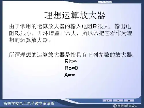
理想运算放大器的主要参数
理想运算放大器是一种具有高增益、带深度负反馈的直接耦合放大器,其主要参数包括:- 开环电压增益Avo:没有反馈的设备增益,理想情况下为无限大。
- 输入电阻ri:指运算放大器在输入级提供的阻抗,理想情况下为无限大。
- 输出电阻ro:指运算放大器在输出级提供的阻抗,理想情况下为零。
- 开环带宽BW:放大器的带宽称为频率范围,理想情况下为无限大。
- 失调电压:指输入端子之间的差分直流电压,理想情况下为零。
- 摆率:如果输入信号有阶跃变化,则运算放大器的摆率是输出信号的变化率,单位是V/ms。
理想情况下为零,意味着输入更改将立即反映在输出中。
这些参数对于理解和设计运算放大器电路至关重要。
在实际应用中,需要根据具体需求和应用场景选择合适的运算放大器,并注意其参数的限制和影响。
vfb与cfb运放用法运放(Operational Amplifier,简称Op Amp)是一种广泛应用于电子电路中的集成电路元件。
它具有高增益、高输入阻抗、低输出阻抗等特点,被广泛应用于信号放大、滤波、比较、积分等电路中。
在运放的应用中,VFB(Voltage Feedback)和CFB(Current Feedback)是两种常见的反馈方式。
VFB运放是指将运放的输出信号通过电阻网络反馈到运放的负输入端,从而控制运放的放大倍数。
这种反馈方式常用于放大电路中,可以实现不同的放大倍数。
在VFB运放中,输出信号经过电阻网络反馈到负输入端,形成一个反馈回路。
通过调整反馈电阻的大小,可以改变运放的放大倍数。
当反馈电阻较大时,运放的放大倍数较小;反之,当反馈电阻较小时,运放的放大倍数较大。
这种方式可以灵活地调整电路的增益,适应不同的应用需求。
CFB运放是指将运放的输出信号通过电流采样电阻反馈到运放的负输入端,从而控制运放的放大倍数。
这种反馈方式常用于高速运算放大器和电流放大器中。
在CFB运放中,输出信号经过电流采样电阻反馈到负输入端,形成一个反馈回路。
通过调整电流采样电阻的大小,可以改变运放的放大倍数。
当电流采样电阻较大时,运放的放大倍数较小;反之,当电流采样电阻较小时,运放的放大倍数较大。
这种方式可以实现高速运算和高精度的电流放大。
VFB和CFB运放在实际应用中各有优势。
VFB运放具有较高的输入阻抗和较低的输出阻抗,适用于需要较高输入阻抗和较低输出阻抗的应用场合。
它在放大电路中应用广泛,可以实现不同的放大倍数,适应不同的信号处理需求。
CFB运放具有较高的带宽和较低的噪声,适用于高速运算和高精度的应用场合。
它在高速运算放大器和电流放大器中应用广泛,可以实现高速运算和高精度的信号处理。
总之,VFB和CFB运放是两种常见的运放反馈方式。
它们在电子电路中具有重要的应用价值。
VFB运放适用于放大电路,可以实现不同的放大倍数;CFB运放适用于高速运算和高精度的应用,可以实现高速运算和高精度的信号处理。
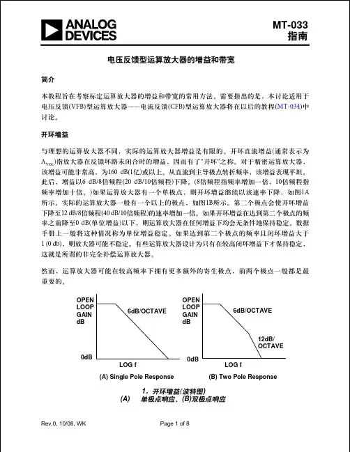
运算放大器之开环增益大多数电压反馈(VFB)型运算放大器的开环电压增益(通常称为AVOL,有时简称 AV)都很高。
常见值从100000到1000000,高精度器件则为该数值的10至100倍。
有些快速运算放大器的开环增益要低得多,但是几千以下的增益不适合高精度应用。
此外还要注意,开环增益对温度变化并不高度稳定,同一类型的不同器件也会存在极大差异,因此,增益值必须很高。
电压反馈运算放大器采用电压输入/电压输出方式工作,其开环增益为无量纲比,所以不需要单位。
但是,数值较小时,为方便起见,数据手册会以V/mV 或V/μV代替V/V表示增益,电压增益也可以dB 形式表示,换算关系为dB = 20×logAVOL。
因此,1V/μV的开环增益相当于120 dB,以此类推。
电流反馈(CFB)型运算放大器采用电流输入和电压输出,因此,其开环跨导增益以V/A或Ω(或kΩ、MΩ)表示。
增益值通常介于几百kΩ与几十MΩ之间。
根据基本反馈原理,为了保持精度,精密放大器的直流开环增益AVOL必须很高。
通过检查闭环增益公式就能发现这点,该公式包含由有限增益引起的误差。
包含有限增益误差的闭环增益公式如下:其中,β是反馈环路衰减,也称反馈因子(反馈网络的电压衰减)。
噪声增益等于1/β,因此,该公式还可以其它形式表示。
将公式右端两项合并,把NG(噪声增益)代入,可得到如下公式:公式1和2是等效的,两者均可使用。
如前所述,噪声增益(NG)只是从与运算放大器输入串联的小电压源获得的增益,是同相模式下的理想放大器信号增益。
如果公式1和2中的AVOL无限大,闭环增益就和噪声增益1/β完全相等。
但是,由于NG <>注意,公式3中的百分比形式增益误差直接与噪声增益成比例(即噪声增益较小时增益误差也较小),因此,有限AVOL对低增益的影响较小。
一些示例可以说明上述增益关系的要点。
〖开环增益不确定性〗下图1中,第一个示例中噪声增益为1000,可以看出,开环增益为200万时,闭环增益误差约为0.05%。
理想运算放大器工作
理想运算放大器(Ideal Operational Amplifier,简称理想运放)是一种虚构的电子元件,它被广泛应用于电子电路设计中。
理想
运放的特点是电压增益无限大、输入阻抗无限大、输出阻抗为零、无
限大的带宽和无限大的公共模抑制比。
在理想情况下,理想运放可以被用于各种应用中。
例如,在放大
器电路中,理想运放可以被用来放大电压信号,从而实现信号放大。
在比较器电路中,理想运算放大器可以被用作一个非常高速的比较器,用于比较两个电压大小。
理想运放的原理是利用微调电路来达到以上特性。
在实际的电路
设计中,理想运放并不存在,但是经过一定的调整和设计,我们可以
将实际运放的性能趋近于理想运放的性能。
理想运放通常有三个输入端,两个输入分别为非反馈输入端和反
馈输入端,还有一个输出端。
其中非反馈输入端一般对应于运放的+输
入端,反馈输入端对应于-输入端。
在运放电路中,负反馈电阻网络可以用来控制电路的输出,从而
使其达到特定的增益。
理想情况下,理想运放的输出电压可以通过此
公式来计算: Vout = A (V+ - V-) ,其中A为电压增益。
如果A趋
近于无限大,那么我们可以得到理想运放的输出电压非常高,甚至可
以使运放输出电压达到电源电压的极限。
总之,理想运算放大器是实际运算放大器的理论基础,有着非常
广泛的应用。
通过对理想运放的研究和应用,我们可以更好地设计实
际电路,从而实现电路的增益、比较等各种功能。
运算放大器基础2009-9-9 9:33:00 【文章字体:大中小】推荐收藏打印运算放大器(简称“运放”)的作用是调节和放大模拟信号。
常见的应用包括数字示波器和自动测试装置、视频和图像计算机板卡、医疗仪器、电视广播设备、航行器用显示器和航空运输控制系统、汽车传感器、计算机工作站和无线基站。
理想的运放理想的运放如图1所示。
通过电阻元件(或者更普遍地通过阻抗元件)施加的负反馈可以产生两种经典的闭环运放配置中的任何一种:反相放大器(图2)和非反相放大器(图3)。
这些配置中的闭环增益的经典等式显示,放大器的增益基本上只取决于反馈元件。
另外,负反馈还可以提供稳定、无失真的输出电压。
电压反馈(VFB)运放电压反馈运放与前文介绍的理想运放一样,它们的输出电压是两个输入端之间电压差的函数。
为设计用途,电压反馈运放的数据表定义5种不同的增益:开环增益(AVOL)、闭环增益、信号增益、噪声增益和环路增益。
负反馈可以改变AVOL 的大小。
对高精度放大器来说,无反馈运放的AVOL值非常大,约为160dB或更高(电压增益为10,000或更高)。
图1:理想的运放。
A VOL 的范围很大,在数据表中它通常以最小/最大值给出。
AVOL还随着电压电平、负载和温度的变化而变化,但这些影响都很小,通常可以忽略不计。
当运放的反馈环路闭合时,它可以提供小于AVOL的闭环增益。
闭环增益有信号增益和噪声增益两种形式。
信号增益(A)指输入信号通过放大器产生的增益,它是电路设计中头等重要的增益。
下面给出了电压反馈电路中信号增益的两个最常见的表达式,它们被广泛用在于反相和同相运放配置中。
图2:反相放大器(a)和非反相放大器(b)是两种经典的闭环运放配置。
对于反相放大器,A = -Rfb /Rin对于同相放大器,A = 1 + Rfb /Rin其中,Rfb 是反馈电阻,Rin是输入电阻。
噪声增益指运放中的噪声源增益,它反映了放大器的输入失调电压和电压噪声对输出的影响。