基于Lattice的LVDS接口调试
- 格式:pdf
- 大小:90.81 KB
- 文档页数:2
基于Altera FPGA的LVDS配置应用一例在特权同学发表博文《Cyclone III的LVDS接口注意事项》后,不少网友发邮件询问LVDS具体应用的一些问题。
这些网友,归根到底,估计是文档看得太少了,或许还缺少动手实践的摸索。
做原型开发的知识储备,无外乎两种方式,要么理论,要么实践。
理论上前面说的文档是一方面,但是说理论不要被文档框住了,以为理论就是书本和文字。
其实换一个角度来理解理论,你也可以认为是间接获得知识的手段,包括一些可用的论坛资源、博文资源,甚至FAE资源等等。
不要金口难开,发个邮件打个电话,可能那些吃这个饭的FAE 们一句话就帮你搞定问题了。
当然了,在你什么都没搞明白前,还是不建议你一通瞎问。
比较合适的方式是先自己去消化官方提供的文档,然后动手实践过程中实在是遇到百思不得其解的问题时再通过请教他人的方式得以解决。
而可能很多“菜鸟”百思不得其解的是文档到底从哪里找,茫茫网络浩如烟海,找个对口文档岂非易事?呵呵,其实,这个文档正可谓“众里寻他千百度,蓦然回首,那人却在灯火阑珊处”。
瞧,有心的朋友早已发现这个不是秘密的秘密了。
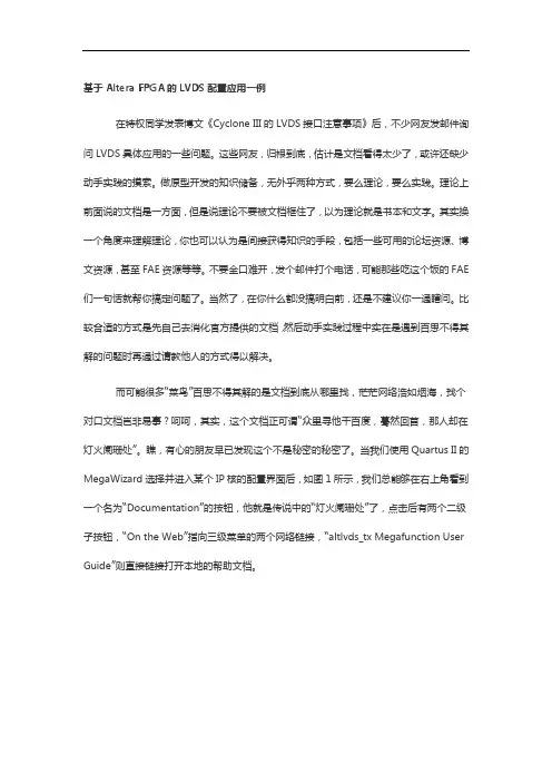
当我们使用Quartus II的MegaWizard选择并进入某个IP核的配置界面后,如图1所示,我们总能够在右上角看到一个名为“Documentation”的按钮,他就是传说中的“灯火阑珊处”了,点击后有两个二级子按钮,“On the Web”指向三级菜单的两个网络链接,“altlvds_tx Megafunction User Guide”则直接链接打开本地的帮助文档。
图1关于文档,除此以外,特权同学比较习惯的做法是在Quartus II handbook或Help 中搜索关键词,如这里的altlvds_tx或LVDS,从而找到相关内容的介绍说明。
在实践前,这些理论知识的储备是必须的,否则咱的“高楼”很可能就是建立在“空穴”之上,指不定哪天就像咱上海前些年那座莲花河畔景苑一样在风雨过后居然楼体完整的“体面”倒下了。
altera的lvds用法Altera(现在归属于英特尔)的FPGA(现在称为Intel FPGA)在实现LVDS(Low Voltage Differential Signaling)时,通常会使用Altera LVDS IP 核或采用LVDS I/O 标准。
下面是一般情况下使用Altera FPGA 实现LVDS 的步骤:1. 引脚规划(Pin Assignment):-在Quartus Prime 设计工具中,打开项目并打开Pin Planner。
-选择LVDS 输入或输出引脚。
-将LVDS 信号与适当的FPGA 引脚相连。
2. 时钟资源分配:-如果LVDS 信号需要与时钟一起使用,确保为LVDS 时钟引脚分配了正确的时钟资源。
- Altera FPGA 提供PLL(Phase-Locked Loop)资源,可用于产生LVDS 时钟。
3. 使用LVDS IP 核:-在Quartus Prime 中,你可以使用IP Catalog 中的"ALTDDIO_IN" 和"ALTDDIO_OUT" IP 核。
-在IP Catalog 中搜索"ALTDDIO_IN" 或"ALTDDIO_OUT",然后将其添加到你的设计中。
-在IP 核配置中,设置LVDS 参数,如输入/输出模式、电压标准等。
4. 约束设置:-在设计中,你可能需要添加SDC(Synopsys Design Constraints)文件,以确保时序约束得到满足。
-针对LVDS 时序进行适当的约束,确保时序满足LVDS 标准。
5. 仿真和验证:-在设计完成后,进行仿真以验证LVDS 信号的正确性。
-使用SignalTap 或其他调试工具来监视LVDS 信号。
6. 生成配置文件和下载到FPGA:-在Quartus Prime 中,使用编译工具生成配置文件。
-使用Programmer 工具将配置文件下载到FPGA 中。
LVDS视频传输数据接口LVDS(Low Voltage Differential Signaling)即低压差分信号传输,是一种满足当今高性能数据传输应用的新型技术。
由于其可使系统供电电压低至 2V,因此它还能满足未来应用的需要。
此技术基于ANSI/TIA/EIA-644 LVDS 接口标准。
LVDS 技术拥有 330mV 的低压差分信号 (250mV MIN and 450mV MAX) 和快速过渡时间。
这可以让产品达到自 100 Mbps 至超过 1 Gbps 的高数据速率。
此外,这种低压摆幅可以降低功耗消散,同时具备差分传输的优点。
由多个数据位和时钟组成的源同步接口已成为电子系统中移动图像数据的一种常用方法。
比较流行的标准是7:1LVDS接口(用于通道链路、平面链路和摄像机链路),它已经成为许多电子产品的通用标准,包括消费设备、工业控制、医疗和汽车远程信息处理。
在这些应用中,使用低成本FPGA进行图像处理的做法已经变得相当普遍。
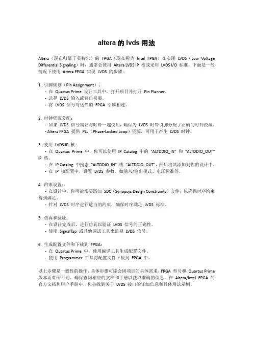
7:1 LVDS接口是一个源同步LVDS接口。
如图1所示,为低速时钟的每个周期序列化7个数据位。
通常,接口由四个(三个数据,一个时钟)或五个(四个数据,一个时钟)LVDS差分对组成。
四对转换为21个并行数据位,五对转换为28个并行数据位。
注意,在时钟上升沿和字边界之间有一个2位偏移。
每个字节有7位长。
图1 7:1LVDS接口每个通道包括一个串行LVDS数据对和一个源同步LVDS时钟对。
接收方接收到该串行LVDS数据,对其进行反序列化,并将其对齐到原始单词边界,生成7个并行LVTTL数据位。
7:1发送器将7个LVTTL 并行数据位串行化为一个LVDS数据位,并将该串行数据通道与LVDS时钟一起传输。
图2显示7:1接收方接收4个LVDS数据通道。
当反序列化时,它生成28位宽的并行数据。
类似地,7:1发送器序列化28位并行数据,生成4个LVDS数据通道。
图2 7:1接收方与发送方基于FPGA的通道链接和平面链接样式接口的需求包括四个关键组件:高速LVDS缓冲区、用于生成反序列化时钟的锁相环、输入数据捕获和传动装置以及数据格式化。
Lattice ispMACH TM 4000V/B/C/Z 设计指南及常见问题解答目录1介绍 (4)1.1特征 (4)1.2产品系列和器件选择手册 (4)1.3性能分析 (5)1.3.1超快性能 (5)1.3.2最低功耗 (6)2体系结构概述 (7)2.1ISP MACH4000体系结构 (7)2.2结构特征 (9)2.2.1逻辑分配器和3种速度路径 (9)2.2.2带可编程延时的输入寄存器 (10)2.2.3灵活的时钟和时钟使能 (10)2.2.4初始化控制 (11)2.2.5ORP BYPASS多路复用器 (11)2.2.6I/O 单元 (12)2.2.7OE 控制 (12)3设计实现 (13)3.1全局约束 (13)3.1.1Fitter 选项 (13)3.1.2利用率选项 (14)3.2约束编辑器 (15)3.2.1设备设置表 (15)3.2.2封装察看/引脚编辑规划 (15)3.2.3引脚/节点位置分配 (16)3.2.4组分配 (16)3.2.5I/O类型设置 (16)3.2.6资源预留 (17)3.2.7缺省设置 (17)3.3资源约束 (17)3.3.1使用源约束注意事项 (17)3.3.2源约束语法 (18)3.4优化设计方法 (21)3.4.1ispLEVEL 约束选项控制 (21)3.4.2HDL 源文件约束控制 (22)4器件应用要点 (22)4.14K系列器件VCC和VCCO的作用和连接 (22)4.24K系列器件各电源上电时间及要求 (22)4.34K系列器件的全局复位 (22)4.4关于4K系列器件时钟的用法 (22)4.5全局输出使能信号 (23)4.6CPLD的I/O口作为双向口使用时应注意的问题 (23)4.7关于设计中使用宽多路复用器的问题 (24)4.8未使用引脚的处理 (25)4.9I/O5V兼容问题 (25)4.10I/O口的电平设置 (25)4.114K系列器件引脚上、下拉电阻,OD,慢摆率特性的设定 (25)4.12关于引脚的缺省值和更改 (27)4.134K系列器件功耗的计算 (27)4.144K系列器件节点温度的计算 (27)4.154K器件的热插拔 (28)4.16ISP JTAG编程/测试信号 (28)4.17CPU加载的频率 (28)4.184K系列器件可承受的加载次数 (28)4.19加载过程中I/O口的状态 (28)4.20综合工具的选择 (29)4.21关于约束文件 (29)4.22用嵌入的M ODEL S IM 仿真 (29)4.23M ODEL S IM应用点滴 (30)4.244K器件上电电压阀值 (30)4.25ISP LEVER中的版本控制功能 (31)4.26ISP LEVER中C ONSTRAINT E DITOR的G LOBAL C ONSTRAINTS设置 (32)4.27ISP LEVER中的时序分析 (33)5ISPLEVER优化参数快速指南 (33)5.1ISP LEVER常用约束优化参数的含义与推荐设置 (33)5.2ISP LEVER推荐的优化参数设置 (35)6ISPLEVER安装说明 (36)6.1ISP LEVER安装说明 (36)6.2ISP VM S YSTEM安装说明 (37)7相关资料 (37)1介绍ispMACH4000 器件包括3.3V、2.5V和1.8V三个系列。
基于UltraFlex系统进行LVDS接口芯片的测试方法苏洋【摘要】The differential signal can be used as high speed interface, LVDS interface can afford high speed translation, the method of testing LVDS interface has great difference form single signal. The paper describe the method of using UltraFlex to test IC with LVDS interface, the content include how to assign ATE channel, how to design DUT PCB and other test techniques. The method is already used for LVDS input and output signal at 800 Mbps.%高速接口通常采用差分信号实现,LVDS接口可以满足高速信号传输,对具备LVDS接口芯片的测试方法与单端信号的测试有较大差别。
描述了如何使用UltraFlex测试系统进行LVDS接口芯片的测试方法,包括通道分配、测试接口板设计和相关测试设置等内容。
此方案已经应用于800 Mbps多路LVDS输入和输出接口的测试。
【期刊名称】《电子与封装》【年(卷),期】2014(000)010【总页数】5页(P4-7,29)【关键词】LVDS;ATE;信号完整性;动态测试向量【作者】苏洋【作者单位】中国电子科技集团公司第58研究所,江苏无锡 214035【正文语种】中文【中图分类】TN407LVDS是一种低摆幅的差分信号技术,LVDS具有高速率、低功耗、抗干扰能力强、低EMI等优点,在高速信号传输中有广泛应用。
第6章Lattice 系列CPLD6.1 概述6.2 CPLD器件系列简介6.1 概述Lattice Semiconductor Corporation 是世界著名的可编程器件厂商,它长期致力于高性能可编程逻辑器件及相关软件的设计、开发和销售。
Lattice可编程器件普遍采用其发明的E2 (电可擦除、电可编程)CMOS工艺和ISP(In System Programmable)技术,具备兼容IEEE 1532标准的在系统可编程性和IEEE 1149.1标准边界扫描可测试性,支持用户直接对安装在电路板上的该类器件进行编程、再编程以及功能与连通性测试,从而在产品的整个生命周期中获得许多利益和方便。
目前,该公司已研制并改进了一系列ISP器件(包括SPLD、CPLD、ispXPLD、FPGA、FPSC)、软件及相关产品,为用户提供了全面的可编程逻辑设计与开发解决方案。
它所提供的ispLEVER设计工具简单易用且支持所有的Lattice可编程逻辑器件,而品种丰富的评估套件/评估板也非常便于用户评估其设计实现,从而加速了其产品开发进程。
ISP 器件及技术的主要优点设计生产用户现场服务,技术支持缩短产品从设计到上市的周期简化系统试制过程提高电路板的可测试性减少器件的实物库存减少生产成本提高系统的质量和可靠性易于在用户现场进行检测和调试经济方便的远程对系统更新和修复6.2 CPLD器件系列简介如表6.1所示,Lattice经过优化的CPLD、XPLD组合包括多种具有不同特点、面向不同应用的器件系列,包括跨越式PLD(MachXO系列)、主流CPLD(ispMACH 4000V/B/C系列)、先进CPLD(ispXPLD5000MV/B/C系列)、5V CPLD(ispMACH4A5系列)、混合信号CPLD (ispPAC-POWR1208/604器件),因而能够提供成本优化和性能领先的解决方案。
表6.1 Lattice CPLD和XPLD器件系列一览表电源系列宏单元t/ns F max/MHz I/O 存储器/Kb PLLPD1.2 V MachXO 128~1140* 3.5 345 73~271 0~27.6 0~2MachXO 128~1140* 3.5 345 73~271 0~27.6 0~25000MC 256~1024 3.5 300 141~381 64~512 2 1.8 V4000C 32~512 2.5 400 30~208 ——4000Z 32~256 3.5 267 32~128 ——MachXO 128~1140* 3.5 345 73~271 0~27.6 0~2 2.5 V5000MB 256~1024 3.5 300 141~381 64~512 24000B 32~512 2.5 400 30~208 ——MachXO 128~1140* 3.5 345 73~271 0~27.6 0~2 3.3 V5000MV 256~1024 3.5 300 141~381 64~512 24000V 32~512 2.5 400 30~208 ——5 V 4A5 32~256 5 182 32~128 ——6.2.1 MachXO跨越式可编程逻辑器件MachXO系列将FPGA的灵活性与CPLD的性能相结合,故被称为跨越式可编程逻辑器件。
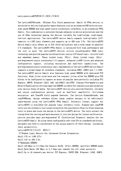
LatticeLatticeECP3PCIE桥接解决方案The LatticeECP3™ (EConomy Plus Third generation) family of FPGA devices is optimized to deliver high perfor-mance features such as an enhanced DSP architecture, high speed SERDES and high speed source synchronous interfaces in an economical FPGA fabric. This combination is achieved through advances in device architecture and the use of 65nm technology making the devices suitable for high-volume, high-speed, low-cost applications. The LatticeECP3 device family expands look-up-table (LUT) capacity to 149K logic elements and supports up to 586 user I/Os. The LatticeECP3 device family also offers up to 320 18x18 multipliers and a wide range of parallel I/O standards. The LatticeECP3 FPGA fabric is optimized with high performance and low cost in mind. The LatticeECP3 devices utilize reconfigurable SRAM logic technology and provide popular building blocks such as LUT-based logic, distrib-uted and embedded memory, Phase Locked Loops (PLLs), Delay Locked Loops (DLLs), pre-engineered source synchronous I/O support, enhanced sysDSP slices and advanced configuration support, including encryption and dual-boot capabilities. The pre-engineered source synchronous logic implemented in the LatticeECP3 device family supports a broad range of interface standards, including DDR3, XGMII and 7:1 LVDS. The LatticeECP3 device family also features high speed SERDES with dedicated PCS functions. High jitter toler-ance and low transmit jitter allow the SERDES plus PCS blocks to be configured to support an array of popular data protocols including PCI Express, SMPTE, Ethernet (XAUI, GbE, and SGMII) and CPRI. Transmit Pre-empha-sis and Receive Equalization settings make the SERDES suitable for transmission and reception over various forms of media. The LatticeECP3 devices also provide flexible, reliable and secure configuration options, such as dual-boot capa-bility, bit-stream encryption, and TransFR field upgrade features. The Lattice Diamond™ and ispLEVER® design software allows large complex designs to be efficiently imple-mented using the LatticeECP3 FPGA family. Synthesis library support for LatticeECP3 is available for popular logic synthesis tools. Diamond and ispLEVER tools use the synthesis tool output along with the constraints from its floor planning tools to place and route the design in the LatticeECP3 device. The tools extract the timing from the routing and back-annotate it into the design for timing verification. Lattice provides many pre-engineered IP (Intellectual Property) modules for the LatticeECP3 family. By using these configurable soft core IPs as standardized blocks, designers are free to concentrate on the unique aspects of their design, increasing their productivity.LatticeECP3器件主要特性:Higher Logic Density for Increased System Integration•17K to 149K LUTs•116 to 586 I/OsEmbedded SERDES•150 Mbps to 3.2 Gbps for Generic 8b10b, 10-bit SERDES, and 8-bit SERDES modes •Data Rates 230 Mbps to 3.2 Gbps per channel for all other protocols•Up to 16 channels per device: PCI Express, SONET/SDH, Ethernet (1GbE, SGMII,XAUI), CPRI, SMPTE 3G and Serial RapidIOsysDSP™•Fully cascadable slice architecture•12 to 160 slices for high performance multiply and accumulate•Powerful 54-bit ALU operations•Time Division Multiplexing MAC Sharing•Rounding and truncation•Each slice supportsFlexible Memory Resources•Up to 6.85Mbits sysMEM™Embedded Block RAM (EBR)•36K to 303K bits distributed RAMsysCLOCK Analog PLLs and DLLs•Two DLLs and up to ten PLLs per devicePre-Engineered Source Synchronous I/O•DDR registers in I/O cells•Dedicated read/write levelling functionality•Dedicated gearing logic•Source synchronous standards support•Dedicated DDR/DDR2/DDR3 memory with DQS support•Optional Inter-Symbol Interference (ISI) correction on outputsProgrammable sysI/O™Buffer Supports Wide Range of Interfaces•On-chip termination•Optional equalization filter on inputs•LVTTL and LVCMOS 33/25/18/15/12•SSTL 33/25/18/15 I, II•HSTL15 I and HSTL18 I, II•PCI and Differential HSTL, SSTL•LVDS, Bus-LVDS, LVPECL, RSDS, MLVDSFlexible Device Configuration•Dedicated bank for configuration I/Os•SPI boot flash interface•Dual-boot images supported•Slave SPI•TransFR™I/O for simple field updates•Soft Error Detect embedded macroSystem Level Support•IEEE 1149.1 and IEEE 1532 compliant•Reveal Logic Analyzer•ORCAstra FPGA configuration utility•On-chip oscillator for initialization & general use•1.2V core power supply图1. LatticeECP3-35 器件简化框图EB43 PCI Express桥接评估板As PCI Express applications have emerged, the LatticeECP3™ FPGA family hasbecome a well-suited solution for many system designs. The features of the LatticeECP3 PCI Express Solutions Board can assist engineers with rapid-prototyping and testing their designs. The board is an enhanced form-factor of the PCI Express add-in card specification. It allows for full x1 form-factor compliance and x4 is available for demonstration purposes with some non-standard form-factor issues. The flexibility to use the same board to demonstrate both x1 and x4 configurations is accomplished by simply changing the mounting hardware. The board has several debugging and analyzing fea-tures for complete evaluation of the LatticeECP3 device. This guide is intended to be referenced in conjunction with evaluation design tutorials to demonstrate the LatticeECP3 FPGA.This user’s guide describes the LatticeECP3 PCI Express Solutions Board featuring the LatticeECP3 LFE3-95EA-FN672 FPGA. The stand-alone evaluation board provides a functional platform for development and rapid prototyp-ing of applications that require high-speed SERDES interfaces to demonstrate PCI Express capabilities using an add-on card form-factor. The board is manufactured using standard FR4 dielectric and through-hole vias. The nom-inal impedance is 50-ohm for single-ended traces and 85-ohm for differential traces.EB43 PCI Express桥接评估板主要特性:• PCI Express x1 and x4 edge connector interfaces• Allows demonstration of PCI Express (x 1and x4) interfaces– x1 is form-factor compliant and will fit a standard PC-equipped PCI Express motherboard socket– x4 is non-compliant but will demonstrate x4 functionality by a simple change to the hardware• Allows control of SERDES PCS registers using the Serial Client Interface (ORCAstra) • On-board Boot Flash– Both Serial SPI Flash and Parallel Flash via MachXO™ programming bridge • Shows interoperation with a high performance DDR2 memory component• Includes driver based “run-time” device configuration capability via ORCAstra or PCI Express• Switches, LEDs, displays for demo purposes• Input connection for lab-power supply• Power connections and power sources• ispVM™ programming support• On-board and external reference clock sources图2.EB43 PCI Express桥接评估板外形图图3.PCI Express桥接解决方案框图图4.EB43 PCI Express桥接评估板电路图(1)图5.EB43 PCI Express桥接评估板电路图(2)图6.EB43 PCI Express桥接评估板电路图(3)图7.EB43 PCI Express桥接评估板电路图(4)图8.EB43 PCI Express桥接评估板电路图(5)图9.EB43 PCI Express桥接评估板电路图(6)图10.EB43 PCI Express桥接评估板电路图(7)图11.EB43 PCI Express桥接评估板电路图(8)图12.EB43 PCI Express桥接评估板电路图(9)EB43 PCI Express桥接评估板材料清单(BOM):图13.EB43 PCI Express桥接评估板元件布局图(顶层)图14.EB43 PCI Express桥接评估板元件布局图(底层) 详情请见:/documents/ds1021ea.pdf和/documents/EB43.pdf。
©LATTICE SEMICONDUCTOR CORPORATIONPage 1Achieving Timing ClosureJohn LiAgenda•Timing closure的概念•Timing closure的步骤•采用合适的Coding Style •进行适当的综合约束•管脚锁定•实施Lattice constrains •Map•布局布线•控制place and route •Floorplanning the design©LATTICE SEMICONDUCTOR CORPORATIONPage 2Timing closure的概念•当前FPGA的设计规模越来越大,复杂程度日益增加,同时要求系统的Perfromace也越来越高。
•获得Timing目标越来越困难.•设计者必须采用各种技术提升系统性能以满足设计的Timing要求.©LATTICE SEMICONDUCTOR CORPORATIONPage 3Timing closure procedure• 1.采用合适的coding style • 2.进行适当的综合约束• 3.管脚锁定• 4.实施Lattice constrains • 5.Map• 5.布局布线•7.控制place and route •8.Floorplanning the design©LATTICE SEMICONDUCTOR CORPORATIONPage 4关于提升FPGA系统性能,工程师最容易想到的方法就是通过进行综合约束、布局布线约束、和其他的优化技术提升系统性能,当然这些都是设计过程中所必需的,但所有这些优化方法对于系统性能的提升都是有限的,系统的性能最终还是取决于工程师的设计(coding style),其中同步设计是最重要的一点. 下面讨论一些具体的coding 技术,合理的运用这些coding技术能够尽可能的减小两级寄存器之间的延时从而获得更高的系统速度.-通用的coding style--Hierarchical Coding---Team Based的设计:多个工程师可以同时参与到一个复杂设计中来。
LatticeLatticeECP27:1LVDS视频接口参考设计方案Lattice公司的LatticeECP2 7:1 LVDS视频评估套件采用LatticeECP2 或LatticeXP2 FPGA,和LatticeECP2高级评估板或LatticeXP2高级评估板以及各种视频I/O源配合使用.本文介绍了LatticeECP2 7:1 接收和发送功能框图, 7:1接收侧和发送侧方框图, LatticeECP2和LatticeXP2 高级评估板的7:1接口测试系统, 视频处理设计案例以及LatticeECP2™高级评估板主要特性,方框图和电路图.The Lattice 7:1 LVDS Video Demo Kit is a set of boards and cables that demonstrate the implementation of a 7:1 LVDS solution using the LatticeECP2 or LatticeXP2 FPGA. The kit works with the LatticeECP2-Advanced Evaluation Board or LatticeXP2 Advanced Evaluation Board, as well as various user video I/O resources.The default design for use with this kit is based on the 7:1 LVDS Video Interface reference design, targeted for the LatticeECP2 or LatticeXP2 FPGA, and specifically tailored for use with this kit. This, and other resources related to this kit can be downloaded from the links at the left of this page.7:1 LVDS视频接口包括:The Lattice 7:1 LVDS Video Demo Kit includes the following:4 Video Demo Boards (See User Manual for full description - link at left of this page)LatticeECP2 Advanced Evaluation Board (Optional - see below)Includes Wall Adapter Power Supply (Universal voltage input, US plugs)Includes ispDOWNLOAD cableBanana Jack Cables (For supplying Power to Video Demo Boards from LatticeECP2 Advanced Evaluation Board or other source)2 Channel-Link MDR CablesDVI Cable图1. LatticeECP2 7:1 LVDS视频接口评估板外形图图2. LatticeECP2 7:1 接收和发送功能图图3.7:1接收侧方框图图4.7:1发送侧方框图图5. LatticeECP2 高级评估板的7:1接口测试系统图6. LatticeXP2 高级评估板的7:1接口测试系统图7.视频处理设计案例LatticeECP2™高级评估板The LatticeECP2 Advanced Evaluation Board provides a convenient platform to evaluate, test and debug user designs and IP cores targeted to the LatticeECP2-50 tticeECP2™高级评估板主要特性:The main features of this board are listed below:• LatticeECP2 FPGA with a 1.2V DC core in a 672-ball fpBGA package (default LatticeECP2-50 FPGA)• SPI Serial Flash device included for low-cost, non-volatile configuration storage• Two 64-bit DDR2 SO-DIMM module connectors (DDR2 DIMMs are not included)• VHDM connectors for SPI4.2 transmit and receive interfaces• Tri-speed (10/100/1000 Mbit) Ethernet PHY that includes RJ-45, magnetics and spark gap• Directly wired RJ-45 connector• Samtec TFM-140-31-S-D-LC connector for interfacing with TI DSP motherboards through the peripheral interface• RS-232 interface chip and 9-pin D-sub connector• USB 1.1 transceiver and USB type-A and type-B connectors• Two 8-bit DIP switches• Discrete LEDs and 7-segment LED• Compact Flash connector for type I and type II Compact Flash cards (Compact Flash cards not included)• LCD module connector (LCD module not included)• Prototyping areas with access to 103 I/O pins• Selectable I/O bank voltages• Four pairs of SMA connectors for high speed differential signals• Oscillator socket for both half-size and full-size oscillators• 3.3V, 2.5V, 1.8V, 1.2V and ADJ (adjustable voltage) powers generated from a single 5V to 28V power source• Power Manager ispPAC-POWR1220AT8 chip for monitoring 3.3V, 2.5V, 1.8V, 1.2V, ADJ voltages and DDR VREF,VTTvoltages• Interface for ispVM System programming supportAlsoIncluded:• 5V/3A AC adapter with international wall plugs• ispDOWNLOAD Cable (HW-DL-3C or equivalent)图tticeECP2™高级评估板方框图图tticeECP2™高级评估板电路图:支持原型图tticeECP2™高级评估板电路图:USB 1.1和RS-232图tticeECP2™高级评估板电路图:编程,开关和LED 图tticeECP2™高级评估板电路图: SPI4.2 Rx图tticeECP2™高级评估板电路图: SPI4.2 Tx图tticeECP2™高级评估板电路图:LCD, CF, IT EMF和OSC图tticeECP2™高级评估板电路图:以太网图tticeECP2™高级评估板电路图: DDR2 SDRAM FPGA图tticeECP2™高级评估板电路图: DDR2 SDRAM SO-DIMM图tticeECP2™高级评估板电路图:FPGA电源引脚图tticeECP2™高级评估板电路图:电源1图tticeECP2™高级评估板电路图:电源2详情请见:/documents/rd1030.pdf和/documents/EB23.pdf。
1.LVDS输出接口概述液晶显示器驱动板输出的数字信号中,除了包括RGB数据信号外,还包括行同步、场同步、像素时钟等信号,其中像素时钟信号的最高频率可超过28MHz。
采用TTL接口,数据传输速率不高,传输距离较短,且抗电磁干扰(EMI)能力也比较差,会对RGB数据造成一定的影响;另外,TTL 多路数据信号采用排线的方式来传送,整个排线数量达几十路,不但连接不便,而且不适合超薄化的趋势。
采用LVDS输出接口传输数据,可以使这些问题迎刃而解,实现数据的高速率、低噪声、远距离、高准确度的传输。
那么,什么是LVDS输出接口呢?LVDS,即Low Voltage Differential Signaling,是一种低压差分信号技术接口。
它是美国NS公司(美国国家半导体公司)为克服以TTL电平方式传输宽带高码率数据时功耗大、EMI电磁干扰大等缺点而研制的一种数字视频信号传输方式。
LVDS输出接口利用非常低的电压摆幅(约350mV)在两条PCB走线或一对平衡电缆上通过差分进行数据的传输,即低压差分信号传输。
采用LVDS输出接口,可以使得信号在差分PCB线或平衡电缆上以几百Mbit/s的速率传输,由于采用低压和低电流驱动方式,因此,实现了低噪声和低功耗。
目前,LVDS输出接口在17in及以上液晶显示器中得到了广泛的应用。
2.LVDS接口电路的组成在液晶显示器中,LVDS接口电路包括两部分,即驱动板侧的LVDS输出接口电路(LVDS发送器)和液晶面板侧的LVDS输入接口电路(LVDS接收器)。
LVDS发送器将驱动板主控芯片输出的17L电平并行RGB数据信号和控制信号转换成低电压串行LVDS信号,然后通过驱动板与液晶面板之间的柔性电缆(排线)将信号传送到液晶面板侧的LVDS接收器,LVDS接收器再将串行信号转换为TTL电平的并行信号,送往液晶屏时序控制与行列驱动电路。
图1所示为LVDS接口电路的组成示意图。
图1 LVDS接口电路的组成示意图在数据传输过程中,还必须有时钟信号的参与,LVDS接口无论传输数据还是传输时钟,都采用差分信号对的形式进行传输。
液晶显示器TL和LVDS接口液晶面板其他信号解析1.TTL接口液晶面板其他信号对于TTL接口液晶面板,其接口信号中,除了前面介绍的RGB数据信号、DCLK时钟信号、行同步信号HS、场同步信号VS、有效数据选通信号DE外,有些还包含以下信号:(1)水平显示模式选择输入信号水平显示模式选择输入信号常用L_R表示,用于控制液晶面板按正常方式还是按水平颠倒方式显示图像。
(2)垂直显示模式选择输入信号垂直显示模式选择输入信号常用U_D表示,用于控制液晶面板按正常方式还是按垂直颠倒方式显示图像。
一般而言,这两个信号即使不接,液晶面板也会正常工作。
(3)电源和接地信号,电源电压一般为3.3V或5V。
2.LVDS接口液晶面板其他信号对于LVDS接口液晶面板,除几对差分数据线(内含串行RGB信号和HS/VS/DE 信号)、一对或两对差分时钟信号线外,有些还包含以下信号:(1)显示模式控制信号有的液晶面板具有显示模式选择功能,通过显示模式控制信号的设置,可以按正常模式、水平颠倒方式或垂直颠倒方式显示图像。
①水平显示模式控制信号(常用L_R表示):用于控制按正常方式还是按水平颠倒方式显示图像。
②垂直显示模式控制信号(常用U_D表示):用于控制按正常方式还是按垂直颠倒方式显示图像。
(2)LVDS格式选择信号有的液晶面板具有适应多种LVDS信号格式(LVDS输出信号格式已在第8章中介绍)的功能,通过LVDS格式选择信号的设置(高电平还是低电平),可以使液晶面板适应液晶显示器驱动板侧LVDS发送芯片输出信号的格式。
LVDS格式选择信号常用SELLVDS来表示,根据需要,可以配置一个或两个LVDS格式选择信号。
当配置一个LVDS格式选择信号时,可以对两种LVDS信号格式进行选择;配置两个LVDS格式选择信号时,可以对三种LVDS信号格式进行选择。
(3)EDID信号EDID即扩展显示器识别数据,在显示器的VGA输入信号接口或DVI信号输入接口中都包含有这种数据。
lattice公司的CrossLink-NX系列是低功耗FPGA,支持各种多种高带宽传感器和显示器接口,视频处理和机器学习推理.采用Lattice公司的Nexus FPGA平台,低功耗28nm FD-SOI技术,组合了极为灵活的FPGA和低功耗以及FD-SOI技术的高可靠性(由于极低SER),提供小占位面积的封装选择. CrossLink-NX系列支持各种接口包括MIPI D-PHY (CSI-2, DSI), LVDS, SLVS, subLVDS, PCI Express (Gen1, Gen2), SGMII(吉比特以太网)等.处理特性包括高达39K逻辑单元,56个18x18乘法器,2.9Mb嵌入存储器(包括EBR和LRAM区块),分布式存储器,DRAM接口(支持DDR3,DDR3L,LPDDR2,LPDDR3高达1066Mbpsx16数据宽度),以及用于软处理器的ALU组成部分.CrossLink-NX系列FPGA支持可配置基于SRAM逻辑架构快速配置,可编sysI/O™ 和TransFR™现场升级特性的超快速配置(不到3ms).安全特性包括比特流加密和密码保护.除了FD-SOI技术固有的高可靠性, 主动可靠性特性还包括内置基于帧的SED/SEC(用于基于SRAM的逻辑架构)和ECC(用于EBR和LRAM),每个器件还内置了ADC,用于系统监视特性.主要用在通信,计算,工业,汽车和消费电子系统的创新嵌入式视觉和AI解决方案.本文介绍了CrossLink-NX FPGA主要特性,CrossLink-NX-40 FPGA简化框图和CrossLink-NX-17 FPGA简化框图与时钟图,以及CrossLink™-NX评估板主要特性,框图,电路图,材料清单和PCB设计图.CrossLink™-NX family of low-power FPGAs can be used in a wide range of applications, and are optimized for bridging and processing needs inEmbedded Vision applications – supporting a variety of high bandwidthsensor and display interfaces, video processing and machine learninginferencing. It is built on Lattice Nexus FPGA platform, using low-power 28 nm FD-SOI technology.It combines the extreme flexibility of an FPGA with the low power and high reliability (due to extremely low SER) of FD-SOI technology, and offers small footprint package options.CrossLink-NX supports a variety of interfaces including MIPI D-PHY(CSI-2, DSI), LVDS, SLVS, subLVDS, PCI Express (Gen1, Gen2), SGMII(Gigabit Ethernet), and more. Processing features of CrossLink-NX include up to 39K Logic Cells, 56 18x18 multipliers, 2.9 Mb of embedded memory (consisting of EBR and LRAM blocks), distributed memory, DRAM interfaces (supporting DDR3, DDR3L, LPDDR2, LPDDR3 up to 1066 Mbps x 16 datawidth), and ALU building blocks for soft processor.CrossLink-NX FPGAs support fast configuration of its reconfigurableSRAM-based logic fabric, ultra-fast configuration (in under 3 ms) of itsprogrammable sysI/O™ and TransFR™ field upgrade feature. Securityfeatures to secure user designs include bitstream encryption and password protection. In addition to the high reliability inherent to FD-SOI technology (due to its extremely low SER), active reliability features such as built-inframe-based SED/SEC (for SRAM-based logic fabric), and ECC (for EBR and LRAM) are also supported. Built-in ADC is available in each device forsystem monitoring functions.Lattice Radiant® design software allows large complex user designs to be efficiently implemented on CrossLink-NX FPGA family.Lattice CrossLink-NX低功耗FPGA嵌入可视和AI应用方案Synthesis library support for CrossLink-NX devices is available forpopular logic synthesis tools. Radiant tools use the synthesis tool output along with constraints from its floor planning tools, to place and route the user design in CrossLink-NX device. The tools extract timing from therouting, and back-annotate it into the design for timing verification.Lattice provides many pre-engineered IP (Intellectual Property)modules for CrossLink-NX family. By using these configurable soft IP cores as standardized blocks, you are free to concentrate on the unique aspects of your design, increasing your productivity.CrossLink-NX FPGA主要特性:· Programmable Architecture· 17K to 39K logic cells· 24 to 56 18 x 18 multipliers (in sysDSP™ blocks)· 2.5 to 2.9 Mb of embedded memory blocks (EBR, LRAM)· 36 to 192 programmable sysI/O (High Performance and Wide Range I/O)· MIPI D-PHY· Up to two hardened 4-lane MIPI D-PHY interfaces· Up to 8 lanes total· Transmit or receive· Supports CSI-2, DSI· 20 Gbps aggregate bandwidth · 2.5Gbps per lane, 10 Gbps per D-PHY interface· Additional Soft D-PHY interfaces supported by High Performance (HP) sysI/O· Transmit or receive· Supports CSI-2, DSI· Up to 1.5 Gbps per lane· Programmable sysI/O supports wide variety of interfaces· High Performance (HP) on bottom I/O dual rank· Supports up to 1.8 V VCCIO· Mixed voltage support (1.0 V, 1.2 V, 1.5 V, 1.8 V)· High-speed differential up to 1.5 Gbps· Supports soft D-PHY (Tx/Rx), LVDS 7:1 (Tx/Rx), SLVS (Tx/Rx), subLVDS (Rx)· Supports SGMII (Gb Ethernet) – 2 channels (Tx/Rx) at 1.25 Gbps· Dedicated DDR3/DDR3L and LPDDR2/LPDDR3 memory support with DQS logic, up to 1066 Mbps data-rate and x16 data-width· Wide Range (WR) on Left, Right and Top I/O Banks· Supports up to 3.3 V VCCIO· Mixed voltage support (1.2 V, 1.5 V, 1.8 V, 2.5 V, 3.3 V)· Programmable slew rate (slow, med, fast)· Controlled impedance mode· Emulated LVDS support· Hot-socketing· Power Modes – Low Power versus High-Performance· User selectable· Low-Power mode for power and/or thermal challenges· High-Performance mode for faster processing· Small footprint package options· 4 x 4 mm2 to 10 x 10 mm2 package options· 2x SGMII CDR at up to 1.25 Gbps – to support 2 channels SGMII using HP I/O· CDR for RX· 8b/10b decoding· Independent Loss of Lock (LOL) detector for each CDR block· sysCLOCK™ analog PLLs· Three in 39K LC and two in 17K LC device· Six outputs per PLL· Fractional N· Programmable and dynamic phase control· sysDSP Enhanced DSP blocks· Hardened pre-adder· Dynamic Shift for AI/ML support· Four 18 x 18, eight 9 x 9, two 18 x 36, or 36 x 36· Advanced 18 x 36, two 18 x 18, or four 8 x 8 MAC · Flexible memory resources· Up to 1.5 Mb sysMEM™ Embedded Block RAM (EBR)· Programmable width· ECC· FIFO· 80k to 240k bits distributed RAM· Large RAM Blocks· 0.5 Mbits per block· Up to five blocks (2.5 Mb total) per device· ALU Features· RISC-V compliant ALU· Register file· SERDES – PCIe Gen2 x1 channel (Tx/Rx) hard IP in 39K LC device · Hard IP supports· Gen1, Gen2, Multi-Function, End Point, Root Complex· APB control bus· AHB-Lite for data bus· Internal bus interface support· APB control bus· AHB-Lite for data bus· AXI4-streaming· Configuration – Fast, Secure· SPI – x1, x2, x4 up to 150 MHz · Master and Slave SPI support · JTAG · I2C and I3C· Ultrafast I/O configuration for instant-on support · Less than 15 ms full device configuration for LIFCL-40· Bitstream Security · Encryption· Single Event Upset (SEU) Mitigation Support· Extremely low Soft Error Rate (SER) due to FD-SOI technology · Soft Error Detect – Embedded hard macro· Soft Error Correction – Without stopping user operation · Soft Error Injection – Emulate SEU event to debug system error handling· ADC – 1 MSPS, 12-bit SAR · 2 ADCs per device· 3 Continuous-time Comparators · Simultaneous sampling · System Level Support· IEEE 1149.1 and IEEE 1532 compliant· Reveal Logic Analyzer· On-chip oscillator for initialization and general use · 1.0 V core power supply图1:CrossLink-NX-40 FPGA 简化框图图2:CrossLink-NX-17 FPGA 简化框图图3. CrossLink-NX FPGA 时钟框图。
ASICS调介退散LVDS接口干扰评估方法改进在现代科技领域,ASICS(Application-Specific Integrated Circuit)已成为关键技术之一。
ASICS常常包含大量的模拟和数字电路,并与其他电子设备进行信号交换。
然而,在设计和使用ASICS时,用户可能会遇到各种干扰问题。
其中,LVDS (Low-Voltage Differential Signaling)接口干扰是一种常见的问题。
本文将探讨一种改进ASICS调介退散LVDS接口干扰评估方法的途径。
首先,我们需要了解ASICS调介退散(crosstalk)和LVDS接口干扰的概念。
调介退散是指信号线之间的相互干扰,通常是由于信号线间的电磁耦合或电容耦合引起的。
而LVDS接口干扰是指低电压差分信号传输时,由于布线不当或引脚设计问题而导致的信号完整性问题。
这两种干扰都可能导致信号质量下降和数据传输错误。
为了改进ASICS调介退散LVDS接口干扰的评估方法,我们可以采用以下步骤:1.仿真模型建立:首先,需要建立适当的仿真模型来模拟ASICS调介退散和LVDS接口干扰的情况。
这包括对ASICS中各个模块的建模以及信号线和接口的参数设置。
在仿真模型中,可以考虑布线方案、引脚布局和输入信号的特性。
2.仿真数据采集:使用建立好的仿真模型,对ASICS进行仿真运行,并采集模拟输出信号。
这些模拟输出信号将用于后续的干扰评估和分析。
3.干扰分析:对仿真采集到的模拟输出信号进行干扰分析。
这包括对信号完整性、干扰峰值和干扰持续时间等方面的评估。
可以使用串扰信号传输指标(crosstalk transfer function)来评估信号之间的干扰程度。
4.参数优化:根据干扰分析的结果,对ASICS的设计参数进行优化。
可以调整布线方案、引脚布局或信号特性等方面的参数。
通过多次仿真和分析的迭代过程,逐步优化ASICS的设计,减少调介退散和LVDS接口干扰。
1 LvdsLow-V oltage Differential Signaling 低压差分信号。
1994年由美国国家半导体公司提出的一种信号传输模式,它是一种标准它在提供高数据传输率的同时会有很低的功耗,另外它还有许多其他的优势:1、低电压电源的兼容性2、低噪声3、高噪声抑制能力4、可靠的信号传输5、能够集成到系统级IC内使用L VDS技术的的产品数据速率可以从几百Mbps到2Gbps。
它是电流驱动的,通过在接收端放置一个负载而得到电压,当电流正向流动,接收端输出为1,反之为0他的摆幅为250mv-450mvL VDS即低压差分信号传输,是一种满足当今高性能数据传输应用的新型技术。
由于其可使系统供电电压低至2V,因此它还能满足未来应用的需要。
此技术基于ANSI/TIA/EIA-644L VDS接口标准。
LVDS技术拥有330mV的低压差分信号(250mVMINand450mVMAX)和快速过渡时间。
这可以让产品达到自100Mbps至超过1Gbps的高数据速率。
此外,这种低压摆幅可以降低功耗消散,同时具备差分传输的优点。
L VDS技术用于简单的线路驱动器和接收器物理层器件以及比较复杂的接口通信芯片组。
通道链路芯片组多路复用和解多路复用慢速TTL信号线路以提供窄式高速低功耗LVDS接口。
这些芯片组可以大幅节省系统的电缆和连接器成本,并且可以减少连接器所占面积所需的物理空间。
L VDS解决方案为设计人员解决高速I/O接口问题提供了新选择。
L VDS为当今和未来的高带宽数据传输应用提供毫瓦每千兆位的方案。
更先进的总线LVDS(BL VDS)是在LVDS基础上面发展起来的,总线LVDS(BLVDS)是基于L VDS技术的总线接口电路的一个新系列,专门用于实现多点电缆或背板应用。
它不同于标准的LVDS,提供增强的驱动电流,以处理多点应用中所需的双重传输。
BLVDS具备大约250mV的低压差分信号以及快速的过渡时间。
基于Lattice的LVDS接口调试
最近因为在实际需求中用LVDS接口,功能为LVDS进,LVDS出。
出去的LVDS线,直接点屏。
一共测试altera xilix latTIce的方案,目标是驱动1080p的LVDS屏。
实际中为了减少飞线的数量,决定采用单路LVDS驱动1080p的屏,实际效果为肯定缺行。
但是无噪点即可。
由于是4个月前的做的,最终选定LatTIce的方案,最终展示的是使用该方案后的效果。
其他两家只做一些分析和改进的建议。
首先评估的使Altera的方案,当时骏龙的FAE很给力,提供了好几块板卡,前后做了一个星期,费了很大的进。
由于当时使用的LVDS的IP,觉得比较稳定。
实现起来应该问题不大。
最终的结果是点屏没有成功,只有图像边缘地方部分区域是亮。
也许是当时对于飞线过于自信,插座飞线到插针,然后再接LVDS插座,在本身FPGA引脚引出的时候用的。
用的使hsmc的插座,应该会有问题,根据后来的现象分析,可能是LVDS引脚没有匹配电阻的问题。
当时的调试现场如下图:。