MAX232芯片使用方法
- 格式:docx
- 大小:97.80 KB
- 文档页数:4
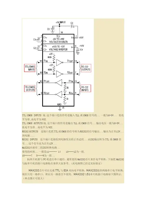
TTL/CMOS INPUTS 端.这个端口是的作用是输入TLL或CMOS信号的...一般为0-5V... 低电平为零,高电平为VCC.TTL/CMOS OUTPUTS端,这个端口的作用是输出TLL或CMOS信号...输出电压一般为0-5V...低电平为零..高电平为VCC.RS232 OUTPUTS 这端口是把TTL或CMOS的信号转为RS232的信号输出...输出为正负12V...到电脑....RS232 INPUTS 这个端口是接收到电脑发出的正负12伏...由232输出转为TTL或CMOS信号...这个信号也为正负12V...MAX232内部有二组232转换电路...使用的时候...一般是11------ 14 13----12为一组.10-----7 8----9为一组...51单片机要与PC机进行串口通信,通常使用MAX232芯片来作电平转换。
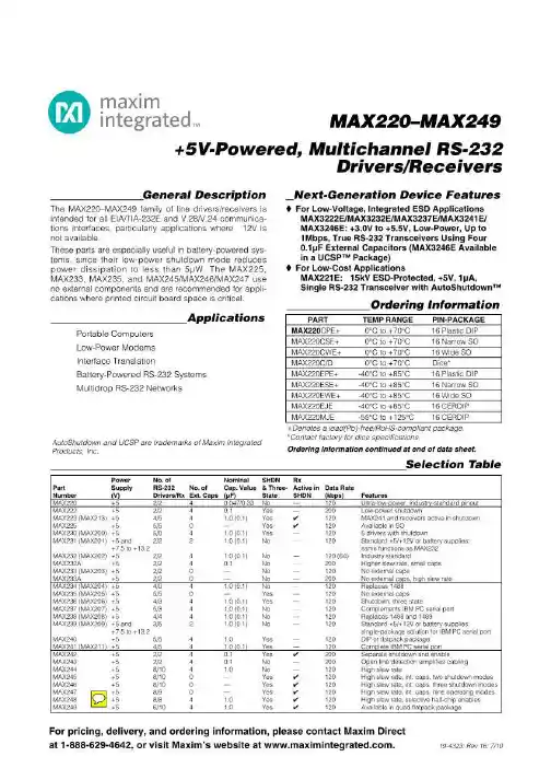
下面把MAX232与51单片机的接口电路贴出来供大家参考。
(此电路图已经过实际验证)MAX232芯片可以完成TTL与EIA双向电平转换,MAX232提供两路串口电平转换,现在只用一路串口,所以另一路悬空不使用,MAX232与51单片机接口电路如下图所示。
(单击图片可放大)图中DB9为串口的插头(母接头),插座共有9个引线.MAX232的12脚接单片机的P3.0(RXD)MAX232的12脚接单片机的P3.1(TXD)MAX232还带有4个电容,都是容量都是104,为了减少电路板体积,可以用无极电容代替极性电容。
VCC 是5V DC提示:串口插座有公母两种类型其中公的串口插座是带有插针的(有针)母的串口插座是不带有插针的(有洞)如下图所示由以上分析可知,DB9为母接头,而电脑PC的串口接头一般是分接头。
所以此电路与PC相连时,所用的串口线应该是一公一母的串口线。
TTL电平信号被利用的最多是因为通常数据表示采用二进制规定,+5V等价于逻辑"1",0V等价于逻辑"0",这被称做TTL(晶体管-晶体管逻辑电平)信号系统,这是计算机处理器控制的设备内部各部分之间通信的标准技术。
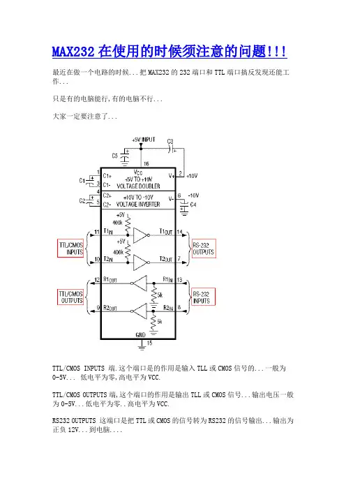
MAX232在使用的时候须注意的问题!!!
最近在做一个电路的时候...把MAX232的232端口和TTL端口搞反发现还能工作...
只是有的电脑能行,有的电脑不行...
大家一定要注意了...
TTL/CMOS INPUTS 端.这个端口是的作用是输入TLL或CMOS信号的...一般为
0-5V... 低电平为零,高电平为VCC.
TTL/CMOS OUTPUTS端,这个端口的作用是输出TLL或CMOS信号...输出电压一般为0-5V...低电平为零..高电平为VCC.
RS232 OUTPUTS 这端口是把TTL或CMOS的信号转为RS232的信号输出...输出为正负12V...到电脑....
RS232 INPUTS 这个端口是接收到电脑发出的正负12伏...由232输出转为TTL 或CMOS信号...这个信号也为正负12V...
MAX232内部有二组232转换电路...
使用的时候...一般是11------ 14 13----12为一组.
10-----7 8----9为一组...
由于有时候接反也能工作....所以大家要用的时候一定要注意了...。
Max232介绍Max232是一款集成电路(IC),通常用于RS-232串行通信接口和微控制器(或其他数字设备)之间的电平转换。
RS-232是一种常见的串行通信标准,用于在不同设备之间传输数据。
然而,RS-232使用的电平范围与微控制器和其他数字设备的标准电平范围不同。
因此,需要一个电平转换器来实现两者之间的通信。
Max232解决了这个问题。
它由内部逻辑电路和电容器组成,可以将低电平转换为高电平,反之亦然,以实现RS-232和微控制器之间的电平转换。
架构Max232由两个逻辑电路组成,每个逻辑电路接受一个RS-232信号和一个电源电压。
一般来说,Max232 IC的供电电压在3.0V到5.5V之间,因此它适用于各种电源电压条件下的应用。
在逻辑电路中,Max232使用了电容器来产生负电压。
通过连接外部电容器,IC可以从正电压源产生一个负电压源。
这个负电压用于将RS-232信号提升到正常的RS-232电平范围。
引脚配置Max232具有16个引脚,按功能可以分成四个组:Vcc和GND•Vcc引脚提供IC的电源电压,通常在3.0V到5.5V之间。
•GND引脚用于接地。
RS-232输入和输出•T1IN和T2OUT是Max232的发送线路。
•R2IN和R1OUT是Max232的接收线路。
电容器连接引脚•C1+和C1-是电容器C1的连接引脚。
•C2+和C2-是电容器C2的连接引脚。
使用方法使用Max232进行电平转换非常简单。
以下是基本的使用步骤:1.将RS-232信号连接到T1IN引脚。
这是需要转换为微控制器可识别电平的信号。
2.将T2OUT引脚连接到微控制器的接收引脚。
这将是接收Max232转换后的信号。
3.链接电容器C1和C2到C1+、C1-和C2+、C2-引脚,以供电和产生负电压。
4.连接Vcc和GND引脚到适当的电源和地线。
完成上述步骤后,Max232将执行电平转换并允许RS-232设备与微控制器进行通信。

MAX232详细资料总结max232 是用来做电平转换的,标准rs232 电平很高,达正负15V.常用的TTL 电平最高5V。
相互连接的话,必须进行电平转换!由于电脑串口输出电压高达12V,直接与单片机连接会烧坏芯片。
所以用MAX232来进行电平转换。
MAX232芯片采用单+5V电源供电,仅需几个外接电容即可完成从TTL到RS232电平的转换,共两路。
其中13脚(R1IN)、12脚(R1OUT)、11脚(T1IN)、14脚(T1OUT)为第一数据通道。
8脚(R2IN)、9脚(R2OUT)、10脚(T2IN)、7脚(T2OUT)为第二数据通道。
TTL/CMOS数据从T1IN、T2IN输入转换成RS-232数据从T1OUT、T2OUT送到电脑DP9插头;DP9插头的RS-232数据从R1IN、R2IN输入转换成TTL/CMOS数据后从R1OUT、R2OUT输出。
MAX232通信电路图单片机中的UART和电脑串口RS232的区别仅在于电平的不同,电脑串口采用232电平,而单片机UART则采用TTL电平,如果不进行电平转换,单片机跟电脑串口就不能进行直接通信,RS232是UART的一种就意味着通信协议的格式是一样的,只要电平统一了,两者之间就可以直接通信,于是乎应用了MAX232这一芯片,MAX232对两者之间通信的数据没有任何作用,仅仅是中介而已,而其只是负责将两者之间的电平进行统一,使两者之间没有通信障碍。
1 TXD 输出数据输出到串口2 DTR_N 输出数据终端准备好,低电平有效3 RST_N 输出发送请求,低电平有效4 VDD_325 电源RS232电源3.3V5 RXD 输入串口数据输入6 RI_N 输入/输出串行端口(环指示器)7 GND 电源接地8 VDD 输入/输出电源9 DSR_N 输入/输出串行端口(数据集就绪)10 DCD_N 输入/输出串行端口(数据载波检测)11 CTS_N 输入/输出串行端口(清除发送)12 SHTD_N 输出控制RS232收发器关机13 EE_CLK 输入/输出串行EEPROM时钟14 EE_DATA 输入/输出串行EEPROM数据15 DP 输入/输出USB端口D+信号16 DM 输入/输出USB端口D-信号17 VO_33常规3.3V电源输出18 GND接地19 RESET复位引脚20 VDD_5 电源USB端口的5V电压电源21 GND接地22 GP0 输入/输出通用I/O引脚023 GP1 输入/输出通用I/O引脚124 VDD_PLL模拟正5v锁相环25 GND_PLL模拟地锁相环26 PLL_TEST 输入PLL锁相环测试模式控制27 OSC1 输入晶体振荡器输入28 OSC2 输入/输出晶体振荡器输出PL2303 是Prolific 公司生产的一种高度集成的RS232-USB 接口转换器,可提供一个RS232 全双工异步串行通信装置与USB 功能接口便利联接的解决方案。
max232是什么芯片MAX232是一种串口转换芯片,用于将TTL(逻辑电平)信号转换成RS232(标准电平)信号。
它广泛应用于计算机硬件通讯领域,如串口通信、电话线调制解调、计算机接口等。
MAX232芯片由Maxim公司设计和生产,是一款双路驱动、双路接收的RS232接口芯片。
它的主要功能是将计算机与其他外设之间的信息转换,以便于计算机与其他设备进行串口通信。
MAX232芯片的主要特点有以下几个方面:1. 低成本:MAX232芯片采用集成电路设计,可以用较低的成本生产出大量的芯片。
2. 双路驱动:MAX232芯片具备双路驱动功能,可以同时驱动两个接收器和两个发射器,适用于双向通信。
3. 兼容性强:MAX232芯片能够将计算机的TTL电平信号转换成RS232标准电平信号,并且在芯片内部进行了自动电平转换,使得计算机与其他设备的通信更加稳定。
4. 外围元件简单:MAX232芯片只需要一些简单的电容器和电阻器作为外围元件,不需要额外的电源供给,减少了系统设计的复杂性。
5. 低功耗:MAX232芯片的功耗较低,适合于在嵌入式系统中使用。
MAX232芯片的工作原理比较简单。
它通过四个电容器和四个电阻器组成一个电压倍增电路,从而将TTL电平(通常为0V和5V)转换为RS232电平(通常为-12V和12V)。
同时,它还能够将RS232电平转换为TTL电平,实现数据的双向传输。
在计算机与外部设备通信时,MAX232芯片的引脚连接如下:1. 引脚2(T1IN)和引脚3(T1OUT)分别连接到计算机的发送线和接收线,用于传输TTL电平信号。
2. 引脚14(R1OUT)和引脚13(R1IN)分别连接到计算机的接收线和发送线,用于接收RS232电平信号。
3. 引脚6(VCC)和引脚11(GND)连接到系统的电源供给线和地线。
4. 引脚7(C1+)和引脚8(C1-)以及引脚5(C2+)和引脚4(C2-)分别连接到对应的电容器和电阻器。
General DescriptionThe MAX220–MAX249 family of line drivers/receivers is intended for all EIA/TIA-232E and V.28/V.24 communica-tions interfaces, particularly applications where ±12V is not available.These parts are especially useful in battery-powered sys-tems, since their low-power shutdown mode reduces power dissipation to less than 5µW. The MAX225,MAX233, MAX235, and MAX245/MAX246/MAX247 use no external components and are recommended for appli-cations where printed circuit board space is critical.________________________ApplicationsPortable Computers Low-Power Modems Interface TranslationBattery-Powered RS-232 Systems Multidrop RS-232 Networks____________________________Features Superior to Bipolaro Operate from Single +5V Power Supply (+5V and +12V—MAX231/MAX239)o Low-Power Receive Mode in Shutdown (MAX223/MAX242)o Meet All EIA/TIA-232E and V.28 Specifications o Multiple Drivers and Receiverso 3-State Driver and Receiver Outputs o Open-Line Detection (MAX243)Ordering InformationOrdering Information continued at end of data sheet.*Contact factory for dice specifications.MAX220–MAX249+5V-Powered, Multichannel RS-232Drivers/Receivers________________________________________________________________Maxim Integrated Products 1Selection Table19-4323; Rev 9; 4/00Power No. of NominalSHDN RxPart Supply RS-232No. of Cap. Value & Three-Active in Data Rate Number (V)Drivers/Rx Ext. Caps (µF)State SHDN (kbps)FeaturesMAX220+52/24 4.7/10No —120Ultra-low-power, industry-standard pinout MAX222+52/2 4 0.1Yes —200Low-power shutdownMAX223 (MAX213)+54/54 1.0 (0.1)Yes ✔120MAX241 and receivers active in shutdown MAX225+55/50—Yes ✔120Available in SOMAX230 (MAX200)+55/04 1.0 (0.1)Yes —120 5 drivers with shutdownMAX231 (MAX201)+5 and2/2 2 1.0 (0.1)No —120Standard +5/+12V or battery supplies; +7.5 to +13.2same functions as MAX232MAX232 (MAX202)+52/24 1.0 (0.1)No —120 (64)Industry standardMAX232A+52/240.1No —200Higher slew rate, small caps MAX233 (MAX203)+52/20— No —120No external capsMAX233A+52/20—No —200No external caps, high slew rate MAX234 (MAX204)+54/04 1.0 (0.1)No —120Replaces 1488MAX235 (MAX205)+55/50—Yes —120No external capsMAX236 (MAX206)+54/34 1.0 (0.1)Yes —120Shutdown, three stateMAX237 (MAX207)+55/34 1.0 (0.1)No —120Complements IBM PC serial port MAX238 (MAX208)+54/44 1.0 (0.1)No —120Replaces 1488 and 1489MAX239 (MAX209)+5 and3/52 1.0 (0.1)No —120Standard +5/+12V or battery supplies;+7.5 to +13.2single-package solution for IBM PC serial port MAX240+55/54 1.0Yes —120DIP or flatpack package MAX241 (MAX211)+54/54 1.0 (0.1)Yes —120Complete IBM PC serial port MAX242+52/240.1Yes ✔200Separate shutdown and enableMAX243+52/240.1No —200Open-line detection simplifies cabling MAX244+58/104 1.0No —120High slew rateMAX245+58/100—Yes ✔120High slew rate, int. caps, two shutdown modes MAX246+58/100—Yes ✔120High slew rate, int. caps, three shutdown modes MAX247+58/90—Yes ✔120High slew rate, int. caps, nine operating modes MAX248+58/84 1.0Yes ✔120High slew rate, selective half-chip enables MAX249+56/1041.0Yes✔120Available in quad flatpack packageFor free samples & the latest literature: , or phone 1-800-998-8800.For small orders, phone 1-800-835-8769.M A X 220–M A X 249+5V-Powered, Multichannel RS-232Drivers/ReceiversABSOLUTE MAXIMUM RATINGS—MAX220/222/232A/233A/242/243ELECTRICAL CHARACTERISTICS—MAX220/222/232A/233A/242/243(V CC = +5V ±10%, C1–C4 = 0.1µF‚ MAX220, C1 = 0.047µF, C2–C4 = 0.33µF, T A = T MIN to T MAX ‚ unless otherwise noted.)Note 1:Input voltage measured with T OUT in high-impedance state, SHDN or V CC = 0V.Note 2:For the MAX220, V+ and V- can have a maximum magnitude of 7V, but their absolute difference cannot exceed 13V.Stresses beyond those listed under “Absolute Maximum Ratings” may cause permanent damage to the device. These are stress ratings only, and functional operation of the device at these or any other conditions beyond those indicated in the operational sections of the specifications is not implied. Exposure to absolute maximum rating conditions for extended periods may affect device reliability.Supply Voltage (V CC )...............................................-0.3V to +6V Input VoltagesT IN ..............................................................-0.3V to (V CC - 0.3V)R IN (Except MAX220)........................................................±30V R IN (MAX220).....................................................................±25V T OUT (Except MAX220) (Note 1).......................................±15V T OUT (MAX220)...............................................................±13.2V Output VoltagesT OUT ...................................................................................±15V R OUT .........................................................-0.3V to (V CC + 0.3V)Driver/Receiver Output Short Circuited to GND.........Continuous Continuous Power Dissipation (T A = +70°C)16-Pin Plastic DIP (derate 10.53mW/°C above +70°C)....842mW 18-Pin Plastic DIP (derate 11.11mW/°C above +70°C)....889mW20-Pin Plastic DIP (derate 8.00mW/°C above +70°C)..440mW 16-Pin Narrow SO (derate 8.70mW/°C above +70°C)...696mW 16-Pin Wide SO (derate 9.52mW/°C above +70°C)......762mW 18-Pin Wide SO (derate 9.52mW/°C above +70°C)......762mW 20-Pin Wide SO (derate 10.00mW/°C above +70°C)....800mW 20-Pin SSOP (derate 8.00mW/°C above +70°C)..........640mW 16-Pin CERDIP (derate 10.00mW/°C above +70°C).....800mW 18-Pin CERDIP (derate 10.53mW/°C above +70°C).....842mW Operating Temperature RangesMAX2_ _AC_ _, MAX2_ _C_ _.............................0°C to +70°C MAX2_ _AE_ _, MAX2_ _E_ _..........................-40°C to +85°C MAX2_ _AM_ _, MAX2_ _M_ _.......................-55°C to +125°C Storage Temperature Range.............................-65°C to +160°C Lead Temperature (soldering, 10sec).............................+300°CMAX220–MAX249+5V-Powered, Multichannel RS-232Drivers/Receivers_______________________________________________________________________________________3Note 3:MAX243 R2OUT is guaranteed to be low when R2IN is ≥0V or is floating.ELECTRICAL CHARACTERISTICS—MAX220/222/232A/233A/242/243 (continued)(V= +5V ±10%, C1–C4 = 0.1µF‚ MAX220, C1 = 0.047µF, C2–C4 = 0.33µF, T = T to T ‚ unless otherwise noted.)M A X 220–M A X 249+5V-Powered, Multichannel RS-232Drivers/Receivers 4_________________________________________________________________________________________________________________________________Typical Operating CharacteristicsMAX220/MAX222/MAX232A/MAX233A/MAX242/MAX243108-1051525OUTPUT VOLTAGE vs. LOAD CURRENT-4-6-8-2642LOAD CURRENT (mA)O U T P U T V O L T A G E (V )1002011104104060AVAILABLE OUTPUT CURRENTvs. DATA RATE65798DATA RATE (kbits/sec)O U T P U T C U R R E N T (m A )203050+10V-10VMAX222/MAX242ON-TIME EXITING SHUTDOWN+5V +5V 0V0V 500µs/div V +, V - V O L T A G E (V )MAX220–MAX249+5V-Powered, Multichannel RS-232Drivers/Receivers_______________________________________________________________________________________5V CC ...........................................................................-0.3V to +6V V+................................................................(V CC - 0.3V) to +14V V-............................................................................+0.3V to -14V Input VoltagesT IN ............................................................-0.3V to (V CC + 0.3V)R IN ......................................................................................±30V Output VoltagesT OUT ...................................................(V+ + 0.3V) to (V- - 0.3V)R OUT .........................................................-0.3V to (V CC + 0.3V)Short-Circuit Duration, T OUT ......................................Continuous Continuous Power Dissipation (T A = +70°C)14-Pin Plastic DIP (derate 10.00mW/°C above +70°C)....800mW 16-Pin Plastic DIP (derate 10.53mW/°C above +70°C)....842mW 20-Pin Plastic DIP (derate 11.11mW/°C above +70°C)....889mW 24-Pin Narrow Plastic DIP(derate 13.33mW/°C above +70°C)..........1.07W24-Pin Plastic DIP (derate 9.09mW/°C above +70°C)......500mW 16-Pin Wide SO (derate 9.52mW/°C above +70°C).........762mW20-Pin Wide SO (derate 10 00mW/°C above +70°C).......800mW 24-Pin Wide SO (derate 11.76mW/°C above +70°C).......941mW 28-Pin Wide SO (derate 12.50mW/°C above +70°C) .............1W 44-Pin Plastic FP (derate 11.11mW/°C above +70°C).....889mW 14-Pin CERDIP (derate 9.09mW/°C above +70°C)..........727mW 16-Pin CERDIP (derate 10.00mW/°C above +70°C)........800mW 20-Pin CERDIP (derate 11.11mW/°C above +70°C)........889mW 24-Pin Narrow CERDIP(derate 12.50mW/°C above +70°C)..............1W24-Pin Sidebraze (derate 20.0mW/°C above +70°C)..........1.6W 28-Pin SSOP (derate 9.52mW/°C above +70°C).............762mW Operating Temperature RangesMAX2 _ _ C _ _......................................................0°C to +70°C MAX2 _ _ E _ _...................................................-40°C to +85°C MAX2 _ _ M _ _ ...............................................-55°C to +125°C Storage Temperature Range.............................-65°C to +160°C Lead Temperature (soldering, 10sec).............................+300°CABSOLUTE MAXIMUM RATINGS—MAX223/MAX230–MAX241ELECTRICAL CHARACTERISTICS—MAX223/MAX230–MAX241(MAX223/230/232/234/236/237/238/240/241, V CC = +5V ±10; MAX233/MAX235, V CC = 5V ±5%‚ C1–C4 = 1.0µF; MAX231/MAX239,V CC = 5V ±10%; V+ = 7.5V to 13.2V; T A = T MIN to T MAX ; unless otherwise noted.)Stresses beyond those listed under “Absolute Maximum Ratings” may cause permanent damage to the device. These are stress ratings only, and functional operation of the device at these or any other conditions beyond those indicated in the operational sections of the specifications is not implied. Exposure to absolute maximum rating conditions for extended periods may affect device reliability.M A X 220–M A X 249+5V-Powered, Multichannel RS-232Drivers/Receivers 6_______________________________________________________________________________________ELECTRICAL CHARACTERISTICS—MAX223/MAX230–MAX241 (continued)(MAX223/230/232/234/236/237/238/240/241, V CC = +5V ±10; MAX233/MAX235, V CC = 5V ±5%‚ C1–C4 = 1.0µF; MAX231/MAX239,V CC = 5V ±10%; V+ = 7.5V to 13.2V; T A = T MIN to T MAX ; unless otherwise noted.)MAX220–MAX249+5V-Powered, Multichannel RS-232Drivers/Receivers_______________________________________________________________________________________78.56.54.55.5TRANSMITTER OUTPUT VOLTAGE (V OH ) vs. V CC7.08.0V CC (V)V O H (V )5.07.57.46.02500TRANSMITTER OUTPUT VOLTAGE (V OH )vs. LOAD CAPACITANCE AT DIFFERENT DATA RATES6.46.27.27.0LOAD CAPACITANCE (pF)V O H (V )1500100050020006.86.612.04.02500TRANSMITTER SLEW RATE vs. LOAD CAPACITANCE6.05.011.09.010.0LOAD CAPACITANCE (pF)S L E W R A T E (V /µs )1500100050020008.07.0-6.0-9.04.55.5TRANSMITTER OUTPUT VOLTAGE (V OL ) vs. V CC-8.0-8.5-6.5-7.0V CC (V)V O L (V )5.0-7.5-6.0-7.62500TRANSMITTER OUTPUT VOLTAGE (V OL )vs. LOAD CAPACITANCE AT DIFFERENT DATA RATES-7.0-7.2-7.4-6.2-6.4LOAD CAPACITANCE (pF)V O L (V )150010005002000-6.6-6.810-105101520253035404550TRANSMITTER OUTPUT VOLTAGE (V+, V-)vs. LOAD CURRENT-2-6-4-886CURRENT (mA)V +, V - (V )420__________________________________________Typical Operating CharacteristicsMAX223/MAX230–MAX241*SHUTDOWN POLARITY IS REVERSED FOR NON MAX241 PARTSV+, V- WHEN EXITING SHUTDOWN(1µF CAPACITORS)MAX220-13SHDN*V-O V+500ms/divM A X 220–M A X 249+5V-Powered, Multichannel RS-232Drivers/Receivers 8_______________________________________________________________________________________ABSOLUTE MAXIMUM RATINGS—MAX225/MAX244–MAX249ELECTRICAL CHARACTERISTICS—MAX225/MAX244–MAX249(MAX225, V CC = 5.0V ±5%; MAX244–MAX249, V CC = +5.0V ±10%, external capacitors C1–C4 = 1µF; T A = T MIN to T MAX ; unless oth-erwise noted.)Note 4:Input voltage measured with transmitter output in a high-impedance state, shutdown, or V CC = 0V.Stresses beyond those listed under “Absolute Maximum Ratings” may cause permanent damage to the device. These are stress ratings only, and functional operation of the device at these or any other conditions beyond those indicated in the operational sections of the specifications is not implied. Exposure to absolute maximum rating conditions for extended periods may affect device reliability.Supply Voltage (V CC )...............................................-0.3V to +6V Input VoltagesT IN ‚ ENA , ENB , ENR , ENT , ENRA ,ENRB , ENTA , ENTB ..................................-0.3V to (V CC + 0.3V)R IN .....................................................................................±25V T OUT (Note 3).....................................................................±15V R OUT ........................................................-0.3V to (V CC + 0.3V)Short Circuit (one output at a time)T OUT to GND............................................................Continuous R OUT to GND............................................................ContinuousContinuous Power Dissipation (T A = +70°C)28-Pin Wide SO (derate 12.50mW/°C above +70°C).............1W 40-Pin Plastic DIP (derate 11.11mW/°C above +70°C)...611mW 44-Pin PLCC (derate 13.33mW/°C above +70°C)...........1.07W Operating Temperature RangesMAX225C_ _, MAX24_C_ _ ..................................0°C to +70°C MAX225E_ _, MAX24_E_ _ ...............................-40°C to +85°C Storage Temperature Range.............................-65°C to +160°C Lead Temperature (soldering,10sec)..............................+300°CMAX220–MAX249+5V-Powered, Multichannel RS-232Drivers/Receivers_______________________________________________________________________________________9Note 5:The 300Ωminimum specification complies with EIA/TIA-232E, but the actual resistance when in shutdown mode or V CC =0V is 10M Ωas is implied by the leakage specification.ELECTRICAL CHARACTERISTICS—MAX225/MAX244–MAX249 (continued)(MAX225, V CC = 5.0V ±5%; MAX244–MAX249, V CC = +5.0V ±10%, external capacitors C1–C4 = 1µF; T A = T MIN to T MAX ; unless oth-erwise noted.)M A X 220–M A X 249+5V-Powered, Multichannel RS-232Drivers/Receivers 10________________________________________________________________________________________________________________________________Typical Operating CharacteristicsMAX225/MAX244–MAX24918212345TRANSMITTER SLEW RATE vs. LOAD CAPACITANCE86416LOAD CAPACITANCE (nF)T R A N S M I T T E R S L E W R A T E (V /µs )14121010-105101520253035OUTPUT VOLTAGEvs. LOAD CURRENT FOR V+ AND V--2-4-6-88LOAD CURRENT (mA)O U T P U T V O L T A G E (V )64209.05.012345TRANSMITTER OUTPUT VOLTAGE (V+, V-)vs. LOAD CAPACITANCE AT DIFFERENT DATA RATES6.05.58.5LOAD CAPACITANCE (nF)V +, V (V )8.07.57.06.5MAX220–MAX249Drivers/Receivers______________________________________________________________________________________11Figure 1. Transmitter Propagation-Delay Timing Figure 2. Receiver Propagation-Delay TimingFigure 3. Receiver-Output Enable and Disable Timing Figure 4. Transmitter-Output Disable TimingM A X 220–M A X 249Drivers/Receivers 12______________________________________________________________________________________ENT ENR OPERATION STATUS TRANSMITTERSRECEIVERS00Normal Operation All Active All Active 01Normal Operation All Active All 3-State10Shutdown All 3-State All Low-Power Receive Mode 11ShutdownAll 3-StateAll 3-StateTable 1a. MAX245 Control Pin ConfigurationsENT ENR OPERATION STATUS TRANSMITTERS RECEIVERSTA1–TA4TB1–TB4RA1–RA5RB1–RB500Normal Operation All Active All Active All Active All Active 01Normal Operation All Active All Active RA1–RA4 3-State,RA5 Active RB1–RB4 3-State,RB5 Active 1ShutdownAll 3-StateAll 3-StateAll Low-Power Receive Mode All Low-Power Receive Mode 11Shutdown All 3-State All 3-StateRA1–RA4 3-State,RA5 Low-Power Receive ModeRB1–RB4 3-State,RB5 Low-Power Receive ModeTable 1b. MAX245 Control Pin ConfigurationsTable 1c. MAX246 Control Pin ConfigurationsENA ENB OPERATION STATUS TRANSMITTERS RECEIVERSTA1–TA4TB1–TB4RA1–RA5RB1–RB500Normal Operation All Active All Active All Active All Active 01Normal Operation All Active All 3-State All Active RB1–RB4 3-State,RB5 Active 1ShutdownAll 3-StateAll ActiveRA1–RA4 3-State,RA5 Active All Active 11Shutdown All 3-State All 3-StateRA1–RA4 3-State,RA5 Low-Power Receive ModeRB1–RB4 3-State,RA5 Low-Power Receive ModeMAX220–MAX249Drivers/Receivers______________________________________________________________________________________13Table 1d. MAX247/MAX248/MAX249 Control Pin ConfigurationsM A X 220–M A X 249_______________Detailed DescriptionThe MAX220–MAX249 contain four sections: dual charge-pump DC-DC voltage converters, RS-232 dri-vers, RS-232 receivers, and receiver and transmitter enable control inputs.Dual Charge-Pump Voltage ConverterThe MAX220–MAX249 have two internal charge-pumps that convert +5V to ±10V (unloaded) for RS-232 driver operation. The first converter uses capacitor C1 to dou-ble the +5V input to +10V on C3 at the V+ output. The second converter uses capacitor C2 to invert +10V to -10V on C4 at the V- output.A small amount of power may be drawn from the +10V (V+) and -10V (V-) outputs to power external circuitry (see the Typical Operating Characteristics section),except on the MAX225 and MAX245–MAX247, where these pins are not available. V+ and V- are not regulated,so the output voltage drops with increasing load current.Do not load V+ and V- to a point that violates the mini-mum ±5V EIA/TIA-232E driver output voltage when sourcing current from V+ and V- to external circuitry. When using the shutdown feature in the MAX222,MAX225, MAX230, MAX235, MAX236, MAX240,MAX241, and MAX245–MAX249, avoid using V+ and V-to power external circuitry. When these parts are shut down, V- falls to 0V, and V+ falls to +5V. For applica-tions where a +10V external supply is applied to the V+pin (instead of using the internal charge pump to gen-erate +10V), the C1 capacitor must not be installed and the SHDN pin must be tied to V CC . This is because V+is internally connected to V CC in shutdown mode.RS-232 DriversThe typical driver output voltage swing is ±8V when loaded with a nominal 5k ΩRS-232 receiver and V CC =+5V. Output swing is guaranteed to meet the EIA/TIA-232E and V.28 specification, which calls for ±5V mini-mum driver output levels under worst-case conditions.These include a minimum 3k Ωload, V CC = +4.5V, and maximum operating temperature. Unloaded driver out-put voltage ranges from (V+ -1.3V) to (V- +0.5V). Input thresholds are both TTL and CMOS compatible.The inputs of unused drivers can be left unconnected since 400k Ωinput pull-up resistors to V CC are built in (except for the MAX220). The pull-up resistors force the outputs of unused drivers low because all drivers invert.The internal input pull-up resistors typically source 12µA,except in shutdown mode where the pull-ups are dis-abled. Driver outputs turn off and enter a high-imped-ance state—where leakage current is typically microamperes (maximum 25µA)—when in shutdownmode, in three-state mode, or when device power is removed. Outputs can be driven to ±15V. The power-supply current typically drops to 8µA in shutdown mode.The MAX220 does not have pull-up resistors to force the ouputs of the unused drivers low. Connect unused inputs to GND or V CC .The MAX239 has a receiver three-state control line, and the MAX223, MAX225, MAX235, MAX236, MAX240,and MAX241 have both a receiver three-state control line and a low-power shutdown control. Table 2 shows the effects of the shutdown control and receiver three-state control on the receiver outputs.The receiver TTL/CMOS outputs are in a high-imped-ance, three-state mode whenever the three-state enable line is high (for the MAX225/MAX235/MAX236/MAX239–MAX241), and are also high-impedance whenever the shutdown control line is high.When in low-power shutdown mode, the driver outputs are turned off and their leakage current is less than 1µA with the driver output pulled to ground. The driver output leakage remains less than 1µA, even if the transmitter output is backdriven between 0V and (V CC + 6V). Below -0.5V, the transmitter is diode clamped to ground with 1k Ωseries impedance. The transmitter is also zener clamped to approximately V CC + 6V, with a series impedance of 1k Ω.The driver output slew rate is limited to less than 30V/µs as required by the EIA/TIA-232E and V.28 specifica-tions. Typical slew rates are 24V/µs unloaded and 10V/µs loaded with 3Ωand 2500pF.RS-232 ReceiversEIA/TIA-232E and V.28 specifications define a voltage level greater than 3V as a logic 0, so all receivers invert.Input thresholds are set at 0.8V and 2.4V, so receivers respond to TTL level inputs as well as EIA/TIA-232E and V.28 levels.The receiver inputs withstand an input overvoltage up to ±25V and provide input terminating resistors withDrivers/Receivers 14Table 2. Three-State Control of ReceiversMAX220–MAX249Drivers/Receivers______________________________________________________________________________________15nominal 5k Ωvalues. The receivers implement Type 1interpretation of the fault conditions of V.28 and EIA/TIA-232E.The receiver input hysteresis is typically 0.5V with a guaranteed minimum of 0.2V. This produces clear out-put transitions with slow-moving input signals, even with moderate amounts of noise and ringing. The receiver propagation delay is typically 600ns and is independent of input swing direction.Low-Power Receive ModeThe low-power receive-mode feature of the MAX223,MAX242, and MAX245–MAX249 puts the IC into shut-down mode but still allows it to receive information. This is important for applications where systems are periodi-cally awakened to look for activity. Using low-power receive mode, the system can still receive a signal that will activate it on command and prepare it for communi-cation at faster data rates. This operation conserves system power.Negative Threshold—MAX243The MAX243 is pin compatible with the MAX232A, differ-ing only in that RS-232 cable fault protection is removed on one of the two receiver inputs. This means that control lines such as CTS and RTS can either be driven or left floating without interrupting communication. Different cables are not needed to interface with different pieces of equipment.The input threshold of the receiver without cable fault protection is -0.8V rather than +1.4V. Its output goes positive only if the input is connected to a control line that is actively driven negative. If not driven, it defaults to the 0 or “OK to send” state. Normally‚ the MAX243’s other receiver (+1.4V threshold) is used for the data line (TD or RD)‚ while the negative threshold receiver is con-nected to the control line (DTR‚ DTS‚ CTS‚ RTS, etc.). Other members of the RS-232 family implement the optional cable fault protection as specified by EIA/TIA-232E specifications. This means a receiver output goes high whenever its input is driven negative‚ left floating‚or shorted to ground. The high output tells the serial communications IC to stop sending data. To avoid this‚the control lines must either be driven or connected with jumpers to an appropriate positive voltage level.Shutdown—MAX222–MAX242On the MAX222‚ MAX235‚ MAX236‚ MAX240‚ and MAX241‚ all receivers are disabled during shutdown.On the MAX223 and MAX242‚ two receivers continue to operate in a reduced power mode when the chip is in shutdown. Under these conditions‚ the propagation delay increases to about 2.5µs for a high-to-low input transition. When in shutdown, the receiver acts as a CMOS inverter with no hysteresis. The MAX223 and MAX242 also have a receiver output enable input (EN for the MAX242 and EN for the MAX223) that allows receiver output control independent of SHDN (SHDN for MAX241). With all other devices‚ SHDN (SH DN for MAX241) also disables the receiver outputs.The MAX225 provides five transmitters and five receivers‚ while the MAX245 provides ten receivers and eight transmitters. Both devices have separate receiver and transmitter-enable controls. The charge pumps turn off and the devices shut down when a logic high is applied to the ENT input. In this state, the supply cur-rent drops to less than 25µA and the receivers continue to operate in a low-power receive mode. Driver outputs enter a high-impedance state (three-state mode). On the MAX225‚ all five receivers are controlled by the ENR input. On the MAX245‚ eight of the receiver out-puts are controlled by the ENR input‚ while the remain-ing two receivers (RA5 and RB5) are always active.RA1–RA4 and RB1–RB4 are put in a three-state mode when ENR is a logic high.Receiver and Transmitter EnableControl InputsThe MAX225 and MAX245–MAX249 feature transmitter and receiver enable controls.The receivers have three modes of operation: full-speed receive (normal active)‚ three-state (disabled)‚ and low-power receive (enabled receivers continue to function at lower data rates). The receiver enable inputs control the full-speed receive and three-state modes. The transmitters have two modes of operation: full-speed transmit (normal active) and three-state (disabled). The transmitter enable inputs also control the shutdown mode. The device enters shutdown mode when all transmitters are disabled. Enabled receivers function in the low-power receive mode when in shutdown.M A X 220–M A X 249Tables 1a–1d define the control states. The MAX244has no control pins and is not included in these tables. The MAX246 has ten receivers and eight drivers with two control pins, each controlling one side of the device. A logic high at the A-side control input (ENA )causes the four A-side receivers and drivers to go into a three-state mode. Similarly, the B-side control input (ENB ) causes the four B-side drivers and receivers to go into a three-state mode. As in the MAX245, one A-side and one B-side receiver (RA5 and RB5) remain active at all times. The entire device is put into shut-down mode when both the A and B sides are disabled (ENA = ENB = +5V).The MAX247 provides nine receivers and eight drivers with four control pins. The ENRA and ENRB receiver enable inputs each control four receiver outputs. The ENTA and ENTB transmitter enable inputs each control four drivers. The ninth receiver (RB5) is always active.The device enters shutdown mode with a logic high on both ENTA and ENTB .The MAX248 provides eight receivers and eight drivers with four control pins. The ENRA and ENRB receiver enable inputs each control four receiver outputs. The ENTA and ENTB transmitter enable inputs control four drivers each. This part does not have an always-active receiver. The device enters shutdown mode and trans-mitters go into a three-state mode with a logic high on both ENTA and ENTB .The MAX249 provides ten receivers and six drivers with four control pins. The ENRA and ENRB receiver enable inputs each control five receiver outputs. The ENTA and ENTB transmitter enable inputs control three dri-vers each. There is no always-active receiver. The device enters shutdown mode and transmitters go into a three-state mode with a logic high on both ENTA and ENTB . In shutdown mode, active receivers operate in a low-power receive mode at data rates up to 20kbits/sec.__________Applications InformationFigures 5 through 25 show pin configurations and typi-cal operating circuits. In applications that are sensitive to power-supply noise, V CC should be decoupled to ground with a capacitor of the same value as C1 and C2 connected as close as possible to the device.Drivers/Receivers16______________________________________________________________________________________。
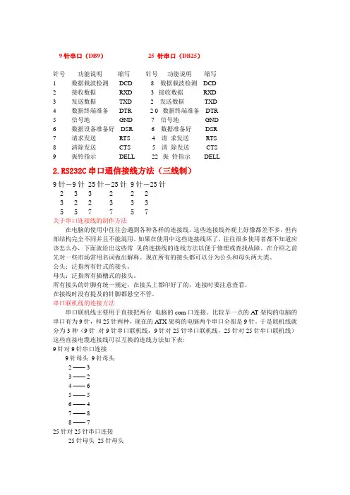
9针串口(DB9)25 针串口(DB25)针号功能说明缩写针号功能说明缩写1 数据载波检测DCD 8 数据载波检测DCD2 接收数据RXD3 接收数据RXD3 发送数据TXD 2 发送数据TXD4 数据终端准备DTR 2 0 数据终端准备DTR5 信号地 GND 7 信号地GND6 数据设备准备好DSR 6 数据准备好DSR7 请求发送RTS 4 请求发送RTS8 清除发送CTS 5 清除发送CTS9 振铃指示DELL 22 振铃指示 DELL2.RS232C串口通信接线方法(三线制)9针-9针 25针-25针 9针-25针2 3 3 2 2 23 2 2 3 3 35 5 7 7 5 7关于串口连接线的制作方法在电脑的使用中往往会遇到各种各样的连接线。
这些连接线外观上好像都差不多,但内部结构完全不同并且不能混用。
如果在使用中这些连接线坏了,往往很多使用者都不知道应该怎么办,下面就给出这些常见的连接线的连线方法以便于修理或查找故障。
在介绍之前先对一些市场常用名词做出解释。
现在所有的接头都可以分为公头和母头两大类。
公头:泛指所有针式的接头。
母头:泛指所有插槽式的接头。
所有接头的针脚有统一规定,在接头上都印好了的,连接时要注意查看。
在接线时没有提及的针脚都悬空不管。
串口联机线的连接方法串口联机线主要用于直接把两台电脑的com口连接。
比较早一点的AT架构的电脑的串口有为9针,和25针两种,现在的ATX架构的电脑两个串口全部是9针。
于是联机线就分为3种(9针对9针串口联机线,9针对25针串口联机线,25针对25针串口联机线)这些直接电缆连接线可以互换的连线方法如下表:9针对9针串口连接9针母头9针母头2 —— 33 —— 24 —— 65 —— 56 —— 47 —— 88 —— 725针对25针串口连接25针母头25针母头2 —— 33 —— 24 —— 55 —— 46 —— 207 —— 720 —— 69针对25针串口连接9针母头25针母头2 —— 23 —— 34 —— 65 —— 76 —— 207 —— 58 —— 4串口转接线这种转接线适用于9针串口和25针串口的转换。
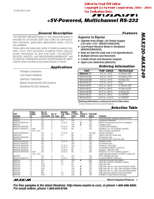
General DescriptionThe MAX220–MAX249 family of line drivers/receivers is intended for all EIA/TIA-232E and V.28/V.24 communica-tions interfaces, particularly applications where ±12V is not available.These parts are especially useful in battery-powered sys-tems, since their low-power shutdown mode reduces power dissipation to less than 5µW. The MAX225,MAX233, MAX235, and MAX245/MAX246/MAX247 use no external components and are recommended for appli-cations where printed circuit board space is critical.________________________ApplicationsPortable Computers Low-Power Modems Interface TranslationBattery-Powered RS-232 Systems Multidrop RS-232 Networks____________________________Features Superior to Bipolaro Operate from Single +5V Power Supply (+5V and +12V—MAX231/MAX239)o Low-Power Receive Mode in Shutdown (MAX223/MAX242)o Meet All EIA/TIA-232E and V.28 Specifications o Multiple Drivers and Receiverso 3-State Driver and Receiver Outputs o Open-Line Detection (MAX243)Ordering InformationOrdering Information continued at end of data sheet.*Contact factory for dice specifications.MAX220–MAX249+5V-Powered, Multichannel RS-232________________________________________________________________Maxim Integrated Products 1Selection Table19-4323; Rev 9; 4/00Power No. of NominalSHDN RxPart Supply RS-232No. of Cap. Value & Three-Active in Data Rate Number (V)Drivers/Rx Ext. Caps (µF)State SHDN (kbps)FeaturesMAX220+52/24 4.7/10No —120Ultra-low-power, industry-standard pinout MAX222+52/2 4 0.1Yes —200Low-power shutdownMAX223 (MAX213)+54/54 1.0 (0.1)Yes ✔120MAX241 and receivers active in shutdown MAX225+55/50—Yes ✔120Available in SOMAX230 (MAX200)+55/04 1.0 (0.1)Yes —120 5 drivers with shutdownMAX231 (MAX201)+5 and2/2 2 1.0 (0.1)No —120Standard +5/+12V or battery supplies; +7.5 to +13.2same functions as MAX232MAX232 (MAX202)+52/24 1.0 (0.1)No —120 (64)Industry standardMAX232A+52/240.1No —200Higher slew rate, small caps MAX233 (MAX203)+52/20— No —120No external capsMAX233A+52/20—No —200No external caps, high slew rate MAX234 (MAX204)+54/04 1.0 (0.1)No —120Replaces 1488MAX235 (MAX205)+55/50—Yes —120No external capsMAX236 (MAX206)+54/34 1.0 (0.1)Yes —120Shutdown, three stateMAX237 (MAX207)+55/34 1.0 (0.1)No —120Complements IBM PC serial port MAX238 (MAX208)+54/44 1.0 (0.1)No —120Replaces 1488 and 1489MAX239 (MAX209)+5 and3/52 1.0 (0.1)No —120Standard +5/+12V or battery supplies;+7.5 to +13.2single-package solution for IBM PC serial port MAX240+55/54 1.0Yes —120DIP or flatpack package MAX241 (MAX211)+54/54 1.0 (0.1)Yes —120Complete IBM PC serial port MAX242+52/240.1Yes ✔200Separate shutdown and enableMAX243+52/240.1No —200Open-line detection simplifies cabling MAX244+58/104 1.0No —120High slew rateMAX245+58/100—Yes ✔120High slew rate, int. caps, two shutdown modes MAX246+58/100—Yes ✔120High slew rate, int. caps, three shutdown modes MAX247+58/90—Yes ✔120High slew rate, int. caps, nine operating modes MAX248+58/84 1.0Yes ✔120High slew rate, selective half-chip enables MAX249+56/1041.0Yes✔120Available in quad flatpack packageFor free samples & the latest literature: , or phone 1-800-998-8800.For small orders, phone 1-800-835-8769.M A X 220–M A X 249+5V-Powered, Multichannel RS-232Drivers/ReceiversABSOLUTE MAXIMUM RATINGS—MAX220/222/232A/233A/242/243ELECTRICAL CHARACTERISTICS—MAX220/222/232A/233A/242/243(V CC = +5V ±10%, C1–C4 = 0.1µF‚ MAX220, C1 = 0.047µF, C2–C4 = 0.33µF, T A = T MIN to T MAX ‚ unless otherwise noted.)Note 1:Input voltage measured with T OUT in high-impedance state, SHDN or V CC = 0V.Note 2:For the MAX220, V+ and V- can have a maximum magnitude of 7V, but their absolute difference cannot exceed 13V.Stresses beyond those listed under “Absolute Maximum Ratings” may cause permanent damage to the device. These are stress ratings only, and functional operation of the device at these or any other conditions beyond those indicated in the operational sections of the specifications is not implied. Exposure to absolute maximum rating conditions for extended periods may affect device reliability.Supply Voltage (V CC )...............................................-0.3V to +6V Input VoltagesT IN ..............................................................-0.3V to (V CC - 0.3V)R IN (Except MAX220)........................................................±30V R IN (MAX220).....................................................................±25V T OUT (Except MAX220) (Note 1).......................................±15V T OUT (MAX220)...............................................................±13.2V Output VoltagesT OUT ...................................................................................±15V R OUT .........................................................-0.3V to (V CC + 0.3V)Driver/Receiver Output Short Circuited to GND.........Continuous Continuous Power Dissipation (T A = +70°C)16-Pin Plastic DIP (derate 10.53mW/°C above +70°C)....842mW 18-Pin Plastic DIP (derate 11.11mW/°C above +70°C)....889mW20-Pin Plastic DIP (derate 8.00mW/°C above +70°C)..440mW 16-Pin Narrow SO (derate 8.70mW/°C above +70°C)...696mW 16-Pin Wide SO (derate 9.52mW/°C above +70°C)......762mW 18-Pin Wide SO (derate 9.52mW/°C above +70°C)......762mW 20-Pin Wide SO (derate 10.00mW/°C above +70°C)....800mW 20-Pin SSOP (derate 8.00mW/°C above +70°C)..........640mW 16-Pin CERDIP (derate 10.00mW/°C above +70°C).....800mW 18-Pin CERDIP (derate 10.53mW/°C above +70°C).....842mW Operating Temperature RangesMAX2_ _AC_ _, MAX2_ _C_ _.............................0°C to +70°C MAX2_ _AE_ _, MAX2_ _E_ _..........................-40°C to +85°C MAX2_ _AM_ _, MAX2_ _M_ _.......................-55°C to +125°C Storage Temperature Range.............................-65°C to +160°C Lead Temperature (soldering, 10sec).............................+300°CMAX220–MAX249+5V-Powered, Multichannel RS-232Drivers/Receivers_______________________________________________________________________________________3Note 3:MAX243 R2OUT is guaranteed to be low when R2IN is ≥0V or is floating.ELECTRICAL CHARACTERISTICS—MAX220/222/232A/233A/242/243 (continued)(V= +5V ±10%, C1–C4 = 0.1µF‚ MAX220, C1 = 0.047µF, C2–C4 = 0.33µF, T = T to T ‚ unless otherwise noted.)M A X 220–M A X 249+5V-Powered, Multichannel RS-232Drivers/Receivers 4_________________________________________________________________________________________________________________________________Typical Operating CharacteristicsMAX220/MAX222/MAX232A/MAX233A/MAX242/MAX243108-1051525OUTPUT VOLTAGE vs. LOAD CURRENT-4-6-8-2642LOAD CURRENT (mA)O U T P U T V O L T A G E (V )1002011104104060AVAILABLE OUTPUT CURRENTvs. DATA RATE65798DATA RATE (kbits/sec)O U T P U T C U R R E N T (m A )203050+10V-10VMAX222/MAX242ON-TIME EXITING SHUTDOWN+5V +5V 0V0V 500µs/div V +, V - V O L T A G E (V )MAX220–MAX249+5V-Powered, Multichannel RS-232Drivers/Receivers_______________________________________________________________________________________5V CC ...........................................................................-0.3V to +6V V+................................................................(V CC - 0.3V) to +14V V-............................................................................+0.3V to -14V Input VoltagesT IN ............................................................-0.3V to (V CC + 0.3V)R IN ......................................................................................±30V Output VoltagesT OUT ...................................................(V+ + 0.3V) to (V- - 0.3V)R OUT .........................................................-0.3V to (V CC + 0.3V)Short-Circuit Duration, T OUT ......................................Continuous Continuous Power Dissipation (T A = +70°C)14-Pin Plastic DIP (derate 10.00mW/°C above +70°C)....800mW 16-Pin Plastic DIP (derate 10.53mW/°C above +70°C)....842mW 20-Pin Plastic DIP (derate 11.11mW/°C above +70°C)....889mW 24-Pin Narrow Plastic DIP(derate 13.33mW/°C above +70°C)..........1.07W24-Pin Plastic DIP (derate 9.09mW/°C above +70°C)......500mW 16-Pin Wide SO (derate 9.52mW/°C above +70°C).........762mW20-Pin Wide SO (derate 10 00mW/°C above +70°C).......800mW 24-Pin Wide SO (derate 11.76mW/°C above +70°C).......941mW 28-Pin Wide SO (derate 12.50mW/°C above +70°C) .............1W 44-Pin Plastic FP (derate 11.11mW/°C above +70°C).....889mW 14-Pin CERDIP (derate 9.09mW/°C above +70°C)..........727mW 16-Pin CERDIP (derate 10.00mW/°C above +70°C)........800mW 20-Pin CERDIP (derate 11.11mW/°C above +70°C)........889mW 24-Pin Narrow CERDIP(derate 12.50mW/°C above +70°C)..............1W24-Pin Sidebraze (derate 20.0mW/°C above +70°C)..........1.6W 28-Pin SSOP (derate 9.52mW/°C above +70°C).............762mW Operating Temperature RangesMAX2 _ _ C _ _......................................................0°C to +70°C MAX2 _ _ E _ _...................................................-40°C to +85°C MAX2 _ _ M _ _ ...............................................-55°C to +125°C Storage Temperature Range.............................-65°C to +160°C Lead Temperature (soldering, 10sec).............................+300°CABSOLUTE MAXIMUM RATINGS—MAX223/MAX230–MAX241ELECTRICAL CHARACTERISTICS—MAX223/MAX230–MAX241(MAX223/230/232/234/236/237/238/240/241, V CC = +5V ±10; MAX233/MAX235, V CC = 5V ±5%‚ C1–C4 = 1.0µF; MAX231/MAX239,V CC = 5V ±10%; V+ = 7.5V to 13.2V; T A = T MIN to T MAX ; unless otherwise noted.)Stresses beyond those listed under “Absolute Maximum Ratings” may cause permanent damage to the device. These are stress ratings only, and functional operation of the device at these or any other conditions beyond those indicated in the operational sections of the specifications is not implied. Exposure to absolute maximum rating conditions for extended periods may affect device reliability.M A X 220–M A X 249+5V-Powered, Multichannel RS-232Drivers/Receivers 6_______________________________________________________________________________________ELECTRICAL CHARACTERISTICS—MAX223/MAX230–MAX241 (continued)(MAX223/230/232/234/236/237/238/240/241, V CC = +5V ±10; MAX233/MAX235, V CC = 5V ±5%‚ C1–C4 = 1.0µF; MAX231/MAX239,V CC = 5V ±10%; V+ = 7.5V to 13.2V; T A = T MIN to T MAX ; unless otherwise noted.)MAX220–MAX249+5V-Powered, Multichannel RS-232Drivers/Receivers_______________________________________________________________________________________78.56.54.55.5TRANSMITTER OUTPUT VOLTAGE (V OH ) vs. V CC7.08.0V CC (V)V O H (V )5.07.57.46.02500TRANSMITTER OUTPUT VOLTAGE (V OH )vs. LOAD CAPACITANCE AT DIFFERENT DATA RATES6.46.27.27.0LOAD CAPACITANCE (pF)V O H (V )1500100050020006.86.612.04.02500TRANSMITTER SLEW RATE vs. LOAD CAPACITANCE6.05.011.09.010.0LOAD CAPACITANCE (pF)S L E W R A T E (V /µs )1500100050020008.07.0-6.0-9.04.55.5TRANSMITTER OUTPUT VOLTAGE (V OL ) vs. V CC-8.0-8.5-6.5-7.0V CC (V)V O L (V )5.0-7.5-6.0-7.62500TRANSMITTER OUTPUT VOLTAGE (V OL )vs. LOAD CAPACITANCE AT DIFFERENT DATA RATES-7.0-7.2-7.4-6.2-6.4LOAD CAPACITANCE (pF)V O L (V )150010005002000-6.6-6.810-105101520253035404550TRANSMITTER OUTPUT VOLTAGE (V+, V-)vs. LOAD CURRENT-2-6-4-886CURRENT (mA)V +, V - (V )420__________________________________________Typical Operating CharacteristicsMAX223/MAX230–MAX241*SHUTDOWN POLARITY IS REVERSED FOR NON MAX241 PARTSV+, V- WHEN EXITING SHUTDOWN(1µF CAPACITORS)MAX220-13SHDN*V-O V+500ms/divM A X 220–M A X 249+5V-Powered, Multichannel RS-232Drivers/Receivers 8_______________________________________________________________________________________ABSOLUTE MAXIMUM RATINGS—MAX225/MAX244–MAX249ELECTRICAL CHARACTERISTICS—MAX225/MAX244–MAX249(MAX225, V CC = 5.0V ±5%; MAX244–MAX249, V CC = +5.0V ±10%, external capacitors C1–C4 = 1µF; T A = T MIN to T MAX ; unless oth-erwise noted.)Note 4:Input voltage measured with transmitter output in a high-impedance state, shutdown, or V CC = 0V.Stresses beyond those listed under “Absolute Maximum Ratings” may cause permanent damage to the device. These are stress ratings only, and functional operation of the device at these or any other conditions beyond those indicated in the operational sections of the specifications is not implied. Exposure to absolute maximum rating conditions for extended periods may affect device reliability.Supply Voltage (V CC )...............................................-0.3V to +6V Input VoltagesT IN ‚ ENA , ENB , ENR , ENT , ENRA ,ENRB , ENTA , ENTB ..................................-0.3V to (V CC + 0.3V)R IN .....................................................................................±25V T OUT (Note 3).....................................................................±15V R OUT ........................................................-0.3V to (V CC + 0.3V)Short Circuit (one output at a time)T OUT to GND............................................................Continuous R OUT to GND............................................................ContinuousContinuous Power Dissipation (T A = +70°C)28-Pin Wide SO (derate 12.50mW/°C above +70°C).............1W 40-Pin Plastic DIP (derate 11.11mW/°C above +70°C)...611mW 44-Pin PLCC (derate 13.33mW/°C above +70°C)...........1.07W Operating Temperature RangesMAX225C_ _, MAX24_C_ _ ..................................0°C to +70°C MAX225E_ _, MAX24_E_ _ ...............................-40°C to +85°C Storage Temperature Range.............................-65°C to +160°C Lead Temperature (soldering,10sec)..............................+300°CMAX220–MAX249+5V-Powered, Multichannel RS-232Drivers/Receivers_______________________________________________________________________________________9Note 5:The 300Ωminimum specification complies with EIA/TIA-232E, but the actual resistance when in shutdown mode or V CC =0V is 10M Ωas is implied by the leakage specification.ELECTRICAL CHARACTERISTICS—MAX225/MAX244–MAX249 (continued)(MAX225, V CC = 5.0V ±5%; MAX244–MAX249, V CC = +5.0V ±10%, external capacitors C1–C4 = 1µF; T A = T MIN to T MAX ; unless oth-erwise noted.)M A X 220–M A X 249+5V-Powered, Multichannel RS-232Drivers/Receivers 10________________________________________________________________________________________________________________________________Typical Operating CharacteristicsMAX225/MAX244–MAX24918212345TRANSMITTER SLEW RATE vs. LOAD CAPACITANCE86416LOAD CAPACITANCE (nF)T R A N S M I T T E R S L E W R A T E (V /µs )14121010-105101520253035OUTPUT VOLTAGEvs. LOAD CURRENT FOR V+ AND V--2-4-6-88LOAD CURRENT (mA)O U T P U T V O L T A G E (V )64209.05.012345TRANSMITTER OUTPUT VOLTAGE (V+, V-)vs. LOAD CAPACITANCE AT DIFFERENT DATA RATES6.05.58.5LOAD CAPACITANCE (nF)V +, V (V )8.07.57.06.5MAX220–MAX249Drivers/Receivers______________________________________________________________________________________11Figure 1. Transmitter Propagation-Delay Timing Figure 2. Receiver Propagation-Delay TimingFigure 3. Receiver-Output Enable and Disable Timing Figure 4. Transmitter-Output Disable TimingM A X 220–M A X 249Drivers/Receivers 12______________________________________________________________________________________ENT ENR OPERATION STATUS TRANSMITTERSRECEIVERS00Normal Operation All Active All Active 01Normal Operation All Active All 3-State10Shutdown All 3-State All Low-Power Receive Mode 11ShutdownAll 3-StateAll 3-StateTable 1a. MAX245 Control Pin ConfigurationsENT ENR OPERATION STATUS TRANSMITTERS RECEIVERSTA1–TA4TB1–TB4RA1–RA5RB1–RB500Normal Operation All Active All Active All Active All Active 01Normal Operation All Active All Active RA1–RA4 3-State,RA5 Active RB1–RB4 3-State,RB5 Active 1ShutdownAll 3-StateAll 3-StateAll Low-Power Receive Mode All Low-Power Receive Mode 11Shutdown All 3-State All 3-StateRA1–RA4 3-State,RA5 Low-Power Receive ModeRB1–RB4 3-State,RB5 Low-Power Receive ModeTable 1b. MAX245 Control Pin ConfigurationsTable 1c. MAX246 Control Pin ConfigurationsENA ENB OPERATION STATUS TRANSMITTERS RECEIVERSTA1–TA4TB1–TB4RA1–RA5RB1–RB500Normal Operation All Active All Active All Active All Active 01Normal Operation All Active All 3-State All Active RB1–RB4 3-State,RB5 Active 1ShutdownAll 3-StateAll ActiveRA1–RA4 3-State,RA5 Active All Active 11Shutdown All 3-State All 3-StateRA1–RA4 3-State,RA5 Low-Power Receive ModeRB1–RB4 3-State,RA5 Low-Power Receive ModeMAX220–MAX249Drivers/Receivers______________________________________________________________________________________13Table 1d. MAX247/MAX248/MAX249 Control Pin ConfigurationsM A X 220–M A X 249_______________Detailed DescriptionThe MAX220–MAX249 contain four sections: dual charge-pump DC-DC voltage converters, RS-232 dri-vers, RS-232 receivers, and receiver and transmitter enable control inputs.Dual Charge-Pump Voltage ConverterThe MAX220–MAX249 have two internal charge-pumps that convert +5V to ±10V (unloaded) for RS-232 driver operation. The first converter uses capacitor C1 to dou-ble the +5V input to +10V on C3 at the V+ output. The second converter uses capacitor C2 to invert +10V to -10V on C4 at the V- output.A small amount of power may be drawn from the +10V (V+) and -10V (V-) outputs to power external circuitry (see the Typical Operating Characteristics section),except on the MAX225 and MAX245–MAX247, where these pins are not available. V+ and V- are not regulated,so the output voltage drops with increasing load current.Do not load V+ and V- to a point that violates the mini-mum ±5V EIA/TIA-232E driver output voltage when sourcing current from V+ and V- to external circuitry. When using the shutdown feature in the MAX222,MAX225, MAX230, MAX235, MAX236, MAX240,MAX241, and MAX245–MAX249, avoid using V+ and V-to power external circuitry. When these parts are shut down, V- falls to 0V, and V+ falls to +5V. For applica-tions where a +10V external supply is applied to the V+pin (instead of using the internal charge pump to gen-erate +10V), the C1 capacitor must not be installed and the SHDN pin must be tied to V CC . This is because V+is internally connected to V CC in shutdown mode.RS-232 DriversThe typical driver output voltage swing is ±8V when loaded with a nominal 5k ΩRS-232 receiver and V CC =+5V. Output swing is guaranteed to meet the EIA/TIA-232E and V.28 specification, which calls for ±5V mini-mum driver output levels under worst-case conditions.These include a minimum 3k Ωload, V CC = +4.5V, and maximum operating temperature. Unloaded driver out-put voltage ranges from (V+ -1.3V) to (V- +0.5V). Input thresholds are both TTL and CMOS compatible.The inputs of unused drivers can be left unconnected since 400k Ωinput pull-up resistors to V CC are built in (except for the MAX220). The pull-up resistors force the outputs of unused drivers low because all drivers invert.The internal input pull-up resistors typically source 12µA,except in shutdown mode where the pull-ups are dis-abled. Driver outputs turn off and enter a high-imped-ance state—where leakage current is typically microamperes (maximum 25µA)—when in shutdownmode, in three-state mode, or when device power is removed. Outputs can be driven to ±15V. The power-supply current typically drops to 8µA in shutdown mode.The MAX220 does not have pull-up resistors to force the ouputs of the unused drivers low. Connect unused inputs to GND or V CC .The MAX239 has a receiver three-state control line, and the MAX223, MAX225, MAX235, MAX236, MAX240,and MAX241 have both a receiver three-state control line and a low-power shutdown control. Table 2 shows the effects of the shutdown control and receiver three-state control on the receiver outputs.The receiver TTL/CMOS outputs are in a high-imped-ance, three-state mode whenever the three-state enable line is high (for the MAX225/MAX235/MAX236/MAX239–MAX241), and are also high-impedance whenever the shutdown control line is high.When in low-power shutdown mode, the driver outputs are turned off and their leakage current is less than 1µA with the driver output pulled to ground. The driver output leakage remains less than 1µA, even if the transmitter output is backdriven between 0V and (V CC + 6V). Below -0.5V, the transmitter is diode clamped to ground with 1k Ωseries impedance. The transmitter is also zener clamped to approximately V CC + 6V, with a series impedance of 1k Ω.The driver output slew rate is limited to less than 30V/µs as required by the EIA/TIA-232E and V.28 specifica-tions. Typical slew rates are 24V/µs unloaded and 10V/µs loaded with 3Ωand 2500pF.RS-232 ReceiversEIA/TIA-232E and V.28 specifications define a voltage level greater than 3V as a logic 0, so all receivers invert.Input thresholds are set at 0.8V and 2.4V, so receivers respond to TTL level inputs as well as EIA/TIA-232E and V.28 levels.The receiver inputs withstand an input overvoltage up to ±25V and provide input terminating resistors withDrivers/Receivers 14Table 2. Three-State Control of ReceiversMAX220–MAX249Drivers/Receivers______________________________________________________________________________________15nominal 5k Ωvalues. The receivers implement Type 1interpretation of the fault conditions of V.28 and EIA/TIA-232E.The receiver input hysteresis is typically 0.5V with a guaranteed minimum of 0.2V. This produces clear out-put transitions with slow-moving input signals, even with moderate amounts of noise and ringing. The receiver propagation delay is typically 600ns and is independent of input swing direction.Low-Power Receive ModeThe low-power receive-mode feature of the MAX223,MAX242, and MAX245–MAX249 puts the IC into shut-down mode but still allows it to receive information. This is important for applications where systems are periodi-cally awakened to look for activity. Using low-power receive mode, the system can still receive a signal that will activate it on command and prepare it for communi-cation at faster data rates. This operation conserves system power.Negative Threshold—MAX243The MAX243 is pin compatible with the MAX232A, differ-ing only in that RS-232 cable fault protection is removed on one of the two receiver inputs. This means that control lines such as CTS and RTS can either be driven or left floating without interrupting communication. Different cables are not needed to interface with different pieces of equipment.The input threshold of the receiver without cable fault protection is -0.8V rather than +1.4V. Its output goes positive only if the input is connected to a control line that is actively driven negative. If not driven, it defaults to the 0 or “OK to send” state. Normally‚ the MAX243’s other receiver (+1.4V threshold) is used for the data line (TD or RD)‚ while the negative threshold receiver is con-nected to the control line (DTR‚ DTS‚ CTS‚ RTS, etc.). Other members of the RS-232 family implement the optional cable fault protection as specified by EIA/TIA-232E specifications. This means a receiver output goes high whenever its input is driven negative‚ left floating‚or shorted to ground. The high output tells the serial communications IC to stop sending data. To avoid this‚the control lines must either be driven or connected with jumpers to an appropriate positive voltage level.Shutdown—MAX222–MAX242On the MAX222‚ MAX235‚ MAX236‚ MAX240‚ and MAX241‚ all receivers are disabled during shutdown.On the MAX223 and MAX242‚ two receivers continue to operate in a reduced power mode when the chip is in shutdown. Under these conditions‚ the propagation delay increases to about 2.5µs for a high-to-low input transition. When in shutdown, the receiver acts as a CMOS inverter with no hysteresis. The MAX223 and MAX242 also have a receiver output enable input (EN for the MAX242 and EN for the MAX223) that allows receiver output control independent of SHDN (SHDN for MAX241). With all other devices‚ SHDN (SH DN for MAX241) also disables the receiver outputs.The MAX225 provides five transmitters and five receivers‚ while the MAX245 provides ten receivers and eight transmitters. Both devices have separate receiver and transmitter-enable controls. The charge pumps turn off and the devices shut down when a logic high is applied to the ENT input. In this state, the supply cur-rent drops to less than 25µA and the receivers continue to operate in a low-power receive mode. Driver outputs enter a high-impedance state (three-state mode). On the MAX225‚ all five receivers are controlled by the ENR input. On the MAX245‚ eight of the receiver out-puts are controlled by the ENR input‚ while the remain-ing two receivers (RA5 and RB5) are always active.RA1–RA4 and RB1–RB4 are put in a three-state mode when ENR is a logic high.Receiver and Transmitter EnableControl InputsThe MAX225 and MAX245–MAX249 feature transmitter and receiver enable controls.The receivers have three modes of operation: full-speed receive (normal active)‚ three-state (disabled)‚ and low-power receive (enabled receivers continue to function at lower data rates). The receiver enable inputs control the full-speed receive and three-state modes. The transmitters have two modes of operation: full-speed transmit (normal active) and three-state (disabled). The transmitter enable inputs also control the shutdown mode. The device enters shutdown mode when all transmitters are disabled. Enabled receivers function in the low-power receive mode when in shutdown.M A X 220–M A X 249Tables 1a–1d define the control states. The MAX244has no control pins and is not included in these tables. The MAX246 has ten receivers and eight drivers with two control pins, each controlling one side of the device. A logic high at the A-side control input (ENA )causes the four A-side receivers and drivers to go into a three-state mode. Similarly, the B-side control input (ENB ) causes the four B-side drivers and receivers to go into a three-state mode. As in the MAX245, one A-side and one B-side receiver (RA5 and RB5) remain active at all times. The entire device is put into shut-down mode when both the A and B sides are disabled (ENA = ENB = +5V).The MAX247 provides nine receivers and eight drivers with four control pins. The ENRA and ENRB receiver enable inputs each control four receiver outputs. The ENTA and ENTB transmitter enable inputs each control four drivers. The ninth receiver (RB5) is always active.The device enters shutdown mode with a logic high on both ENTA and ENTB .The MAX248 provides eight receivers and eight drivers with four control pins. The ENRA and ENRB receiver enable inputs each control four receiver outputs. The ENTA and ENTB transmitter enable inputs control four drivers each. This part does not have an always-active receiver. The device enters shutdown mode and trans-mitters go into a three-state mode with a logic high on both ENTA and ENTB .The MAX249 provides ten receivers and six drivers with four control pins. The ENRA and ENRB receiver enable inputs each control five receiver outputs. The ENTA and ENTB transmitter enable inputs control three dri-vers each. There is no always-active receiver. The device enters shutdown mode and transmitters go into a three-state mode with a logic high on both ENTA and ENTB . In shutdown mode, active receivers operate in a low-power receive mode at data rates up to 20kbits/sec.__________Applications InformationFigures 5 through 25 show pin configurations and typi-cal operating circuits. In applications that are sensitive to power-supply noise, V CC should be decoupled to ground with a capacitor of the same value as C1 and C2 connected as close as possible to the device.Drivers/Receivers16______________________________________________________________________________________。
max232是一种把电脑的串行口rs232信号电平(-10 ,+10v)转换为单片机所用到的TTL信号点平(0 ,+5)的芯片,这个芯片的价格比较贵大约要6元,下面我来介绍一下max232引脚图以及max232和电脑串口的连接电路,RS232引脚定义。
看下面的图。
《max232引脚图》《max232电路》《RS232引脚定义》引脚定义符号1 载波检测 DCD2 接收数据 RXD3 发送数据 TXD4 数据终端准备好 DTR5 信号地 SG6 数据准备好 DSR7 请求发送 RTS8 清除发送 CTS9 振铃提示 RI希望上面的资料对你有用。
MAX232转RS485-红外转发器---很方便的通讯协议调试工具主要功能:集RS485通讯与红外通讯与1体;方便调试软件及日常通讯功能,只使用一个串口。
呵呵,节省的时间可以做很多事。
通用型MAX232-RS485-红外通讯有源光隔转换器产品简介:实现RS-232与RS-485、红外有源光隔转换,支持远程通信(RS485大于1.5Km,红外大于6m)和多机通信(32接点),半双工,不需外加5V 电源。
产品特性:MAX-232/RS-485、红外转换,标准DB9孔串独有串口保护电路,可带电热插拔内置600W/ms抗雷击保护和15KV抗静电保护透明传输,波特率自适应,无需更改用户协议工业级设计,优选进口元器件,全部表面贴装工艺技术指标:工作电流:<10mA波特率: 300-115.2Kbps 通信距离: 0-1.5Km保护动作电压: 7-8V保护动作容量: 600W/ms 静电保护电压: 15KV工作温度: -45℃~85℃。
M A X232原理及应用RS232 (DB9)引脚定义1 :DCD :载波检测。
主要用于Modem通知计算机其处于在线状态,即Modem检测到拨号音,处于在线状态。
2 :RXD:此引脚用于接收外部设备送来的数据;在你使用Modem时,你会发现RXD指示灯在闪烁,说明RXD引脚上有数据进入。
3 :TXD:此引脚将计算机的数据发送给外部设备;在你使用Modem 时,你会发现TXD指示灯在闪烁,说明计算机正在通过TXD引脚发送数据。
4 :DTR:数据终端就绪;当此引脚高电平时,通知Modem可以进行数据传输,计算机已经准备好。
5 :GND:信号地;此位不做过多解释。
6 :DSR:数据设备就绪;此引脚高电平时,通知计算机Modem已经准备好,可以进行数据通讯了。
7 :RTS:请求发送;此脚由计算机来控制,用以通知Modem马上传送数据至计算机;否则,Modem将收到的数据暂时放入缓冲区中。
8 :CTS: 清除发送;此脚由Modem控制,用以通知计算机将欲传的数据送至Modem。
9 :RI : Modem通知计算机有呼叫进来,是否接听呼叫由计算机决定MAX232原理MAX232芯片是专门为电脑的RS-232标准串口设计的接口电路,使用+5v单电源供电。
内部结构基本可分三个部分:第一部分是电荷泵电路。
由1、2、3、4、5、6脚和4只电容构成。
功能是产生+12v和-12v两个电源,提供给RS-232串口电平的需要。
第二部分是数据转换通道。
由7、8、9、10、11、12、13、14脚构成两个数据通道。
其中13脚(R1IN)、12脚(R1OUT)、11脚(T1IN)、14脚(T1OUT)为第一数据通道。
8脚(R2IN)、9脚(R2OUT)、10脚(T2IN)、7脚(T2OUT)为第二数据通道。
TTL/CMOS数据从T1IN、T2IN输入转换成RS-232数据从T1OUT、T2OUT送到电脑DP9插头;DP9插头的RS-232数据从R1IN、R2IN 输入转换成TTL/CMOS数据后从R1OUT、R2OUT输出。
12V转TTL电平可以使用电平转换器或移位寄存器来实现。
一种常见的方法是使用MAX232芯片或其他类似的芯片将12V的电平转换为TTL电平。
MAX232芯片有4个通道,每个通道提供一个TTL输入和一个TTL输出。
连接12V电源到芯片的VCC和GND引脚,然后将12V输入信号连接到一个通道的TTL输入引脚,该通道的TTL输出就是转换后的TTL电平信号。
电平转换电路主要由电源、电阻、电容、二极管和集成电路等元器件组成。
其中,电源提供12V电压,电阻和电容用于限流和滤波,二极管用于保护电路,集成电路则是实现电压转换的核心部件。
当12V电压通过电路时,集成电路将电压转换为TTL电平。
以上信息仅供参考,如需了解更多信息,建议查阅专业书籍或咨询专业人士。
General DescriptionThe MAX220–MAX249 family of line drivers/receivers is intended for all EIA/TIA-232E and V.28/V.24 communica-tions interfaces, particularly applications where ±12V is not available.These parts are especially useful in battery-powered sys-tems, since their low-power shutdown mode reduces power dissipation to less than 5µW. The MAX225,MAX233, MAX235, and MAX245/MAX246/MAX247 use no external components and are recommended for appli-cations where printed circuit board space is critical.________________________ApplicationsPortable Computers Low-Power Modems Interface TranslationBattery-Powered RS-232 Systems Multidrop RS-232 Networks____________________________Features Superior to Bipolaro Operate from Single +5V Power Supply (+5V and +12V—MAX231/MAX239)o Low-Power Receive Mode in Shutdown (MAX223/MAX242)o Meet All EIA/TIA-232E and V.28 Specifications o Multiple Drivers and Receiverso 3-State Driver and Receiver Outputs o Open-Line Detection (MAX243)Ordering InformationOrdering Information continued at end of data sheet.*Contact factory for dice specifications.MAX220–MAX249+5V-Powered, Multichannel RS-232Drivers/Receivers________________________________________________________________Maxim Integrated Products 1Selection Table19-4323; Rev 9; 4/00Power No. ofNominalSHDN RxPart Supply RS-232No. of Cap. Value & Three-Active in Data Rate Number (V)Drivers/Rx Ext. Caps (µF)State SHDN (kbps)FeaturesMAX220+52/24 4.7/10No —120Ultra-low-power, industry-standard pinout MAX222+52/2 4 0.1Yes —200Low-power shutdownMAX223 (MAX213)+54/54 1.0 (0.1)Yes ✔120MAX241 and receivers active in shutdown MAX225+55/50—Yes ✔120Available in SOMAX230 (MAX200)+55/04 1.0 (0.1)Yes —120 5 drivers with shutdownMAX231 (MAX201)+5 and2/2 2 1.0 (0.1)No —120Standard +5/+12V or battery supplies; +7.5 to +13.2same functions as MAX232MAX232 (MAX202)+52/24 1.0 (0.1)No —120 (64)Industry standardMAX232A+52/240.1No —200Higher slew rate, small caps MAX233 (MAX203)+52/20— No —120No external capsMAX233A+52/20—No —200No external caps, high slew rate MAX234 (MAX204)+54/04 1.0 (0.1)No —120Replaces 1488MAX235 (MAX205)+55/50—Yes —120No external capsMAX236 (MAX206)+54/34 1.0 (0.1)Yes —120Shutdown, three stateMAX237 (MAX207)+55/34 1.0 (0.1)No —120Complements IBM PC serial port MAX238 (MAX208)+54/44 1.0 (0.1)No —120Replaces 1488 and 1489MAX239 (MAX209)+5 and3/52 1.0 (0.1)No —120Standard +5/+12V or battery supplies;+7.5 to +13.2single-package solution for IBM PC serial port MAX240+55/54 1.0Yes —120DIP or flatpack package MAX241 (MAX211)+54/54 1.0 (0.1)Yes —120Complete IBM PC serial port MAX242+52/240.1Yes ✔200Separate shutdown and enableMAX243+52/240.1No —200Open-line detection simplifies cabling MAX244+58/104 1.0No —120High slew rateMAX245+58/100—Yes ✔120High slew rate, int. caps, two shutdown modes MAX246+58/100—Yes ✔120High slew rate, int. caps, three shutdown modes MAX247+58/90—Yes ✔120High slew rate, int. caps, nine operating modes MAX248+58/84 1.0Yes ✔120High slew rate, selective half-chip enables MAX249+56/1041.0Yes✔120Available in quad flatpack packageFor free samples & the latest literature: , or phone 1-800-998-8800.For small orders, phone 1-800-835-8769.M A X 220–M A X 249+5V-Powered, Multichannel RS-232Drivers/ReceiversABSOLUTE MAXIMUM RATINGS—MAX220/222/232A/233A/242/243ELECTRICAL CHARACTERISTICS—MAX220/222/232A/233A/242/243(V CC = +5V ±10%, C1–C4 = 0.1µF‚ MAX220, C1 = 0.047µF, C2–C4 = 0.33µF, T A = T MIN to T MAX ‚ unless otherwise noted.)Note 1:Input voltage measured with T OUT in high-impedance state, SHDN or V CC = 0V.Note 2:For the MAX220, V+ and V- can have a maximum magnitude of 7V, but their absolute difference cannot exceed 13V.Stresses beyond those listed under “Absolute Maximum Ratings” may cause permanent damage to the device. These are stress ratings only, and functional operation of the device at these or any other conditions beyond those indicated in the operational sections of the specifications is not implied. Exposure to absolute maximum rating conditions for extended periods may affect device reliability.Supply Voltage (V CC )...............................................-0.3V to +6V Input VoltagesT IN ..............................................................-0.3V to (V CC - 0.3V)R IN (Except MAX220)........................................................±30V R IN (MAX220).....................................................................±25V T OUT (Except MAX220) (Note 1).......................................±15V T OUT (MAX220)...............................................................±13.2V Output VoltagesT OUT ...................................................................................±15V R OUT .........................................................-0.3V to (V CC + 0.3V)Driver/Receiver Output Short Circuited to GND.........Continuous Continuous Power Dissipation (T A = +70°C)16-Pin Plastic DIP (derate 10.53mW/°C above +70°C)....842mW 18-Pin Plastic DIP (derate 11.11mW/°C above +70°C)....889mW20-Pin Plastic DIP (derate 8.00mW/°C above +70°C)..440mW 16-Pin Narrow SO (derate 8.70mW/°C above +70°C)...696mW 16-Pin Wide SO (derate 9.52mW/°C above +70°C)......762mW 18-Pin Wide SO (derate 9.52mW/°C above +70°C)......762mW 20-Pin Wide SO (derate 10.00mW/°C above +70°C)....800mW 20-Pin SSOP (derate 8.00mW/°C above +70°C)..........640mW 16-Pin CERDIP (derate 10.00mW/°C above +70°C).....800mW 18-Pin CERDIP (derate 10.53mW/°C above +70°C).....842mW Operating Temperature RangesMAX2_ _AC_ _, MAX2_ _C_ _.............................0°C to +70°C MAX2_ _AE_ _, MAX2_ _E_ _..........................-40°C to +85°C MAX2_ _AM_ _, MAX2_ _M_ _.......................-55°C to +125°C Storage Temperature Range.............................-65°C to +160°C Lead Temperature (soldering, 10sec).............................+300°CMAX220–MAX249+5V-Powered, Multichannel RS-232Drivers/Receivers_______________________________________________________________________________________3Note 3:MAX243 R2OUT is guaranteed to be low when R2IN is ≥0V or is floating.ELECTRICAL CHARACTERISTICS—MAX220/222/232A/233A/242/243 (continued)(V= +5V ±10%, C1–C4 = 0.1µF‚ MAX220, C1 = 0.047µF, C2–C4 = 0.33µF, T = T to T ‚ unless otherwise noted.)M A X 220–M A X 249+5V-Powered, Multichannel RS-232Drivers/Receivers 4_________________________________________________________________________________________________________________________________Typical Operating CharacteristicsMAX220/MAX222/MAX232A/MAX233A/MAX242/MAX243108-1051525OUTPUT VOLTAGE vs. LOAD CURRENT-4-6-8-2642LOAD CURRENT (mA)O U T P U T V O L T A G E (V )1002011104104060AVAILABLE OUTPUT CURRENTvs. DATA RATE65798DATA RATE (kbits/sec)O U T P U T C U R R E N T (m A )203050+10V-10VMAX222/MAX242ON-TIME EXITING SHUTDOWN+5V +5V 0V0V 500µs/div V +, V - V O L T A G E (V )MAX220–MAX249+5V-Powered, Multichannel RS-232Drivers/Receivers_______________________________________________________________________________________5V CC ...........................................................................-0.3V to +6V V+................................................................(V CC - 0.3V) to +14V V-............................................................................+0.3V to -14V Input VoltagesT IN ............................................................-0.3V to (V CC + 0.3V)R IN ......................................................................................±30V Output VoltagesT OUT ...................................................(V+ + 0.3V) to (V- - 0.3V)R OUT .........................................................-0.3V to (V CC + 0.3V)Short-Circuit Duration, T OUT ......................................Continuous Continuous Power Dissipation (T A = +70°C)14-Pin Plastic DIP (derate 10.00mW/°C above +70°C)....800mW 16-Pin Plastic DIP (derate 10.53mW/°C above +70°C)....842mW 20-Pin Plastic DIP (derate 11.11mW/°C above +70°C)....889mW 24-Pin Narrow Plastic DIP(derate 13.33mW/°C above +70°C)..........1.07W24-Pin Plastic DIP (derate 9.09mW/°C above +70°C)......500mW 16-Pin Wide SO (derate 9.52mW/°C above +70°C).........762mW20-Pin Wide SO (derate 10 00mW/°C above +70°C).......800mW 24-Pin Wide SO (derate 11.76mW/°C above +70°C).......941mW 28-Pin Wide SO (derate 12.50mW/°C above +70°C) .............1W 44-Pin Plastic FP (derate 11.11mW/°C above +70°C).....889mW 14-Pin CERDIP (derate 9.09mW/°C above +70°C)..........727mW 16-Pin CERDIP (derate 10.00mW/°C above +70°C)........800mW 20-Pin CERDIP (derate 11.11mW/°C above +70°C)........889mW 24-Pin Narrow CERDIP(derate 12.50mW/°C above +70°C)..............1W24-Pin Sidebraze (derate 20.0mW/°C above +70°C)..........1.6W 28-Pin SSOP (derate 9.52mW/°C above +70°C).............762mW Operating Temperature RangesMAX2 _ _ C _ _......................................................0°C to +70°C MAX2 _ _ E _ _...................................................-40°C to +85°C MAX2 _ _ M _ _ ...............................................-55°C to +125°C Storage Temperature Range.............................-65°C to +160°C Lead Temperature (soldering, 10sec).............................+300°CABSOLUTE MAXIMUM RATINGS—MAX223/MAX230–MAX241ELECTRICAL CHARACTERISTICS—MAX223/MAX230–MAX241(MAX223/230/232/234/236/237/238/240/241, V CC = +5V ±10; MAX233/MAX235, V CC = 5V ±5%‚ C1–C4 = 1.0µF; MAX231/MAX239,V CC = 5V ±10%; V+ = 7.5V to 13.2V; T A = T MIN to T MAX ; unless otherwise noted.)Stresses beyond those listed under “Absolute Maximum Ratings” may cause permanent damage to the device. These are stress ratings only, and functional operation of the device at these or any other conditions beyond those indicated in the operational sections of the specifications is not implied. Exposure to absolute maximum rating conditions for extended periods may affect device reliability.M A X 220–M A X 249+5V-Powered, Multichannel RS-232Drivers/Receivers 6_______________________________________________________________________________________ELECTRICAL CHARACTERISTICS—MAX223/MAX230–MAX241 (continued)(MAX223/230/232/234/236/237/238/240/241, V CC = +5V ±10; MAX233/MAX235, V CC = 5V ±5%‚ C1–C4 = 1.0µF; MAX231/MAX239,V CC = 5V ±10%; V+ = 7.5V to 13.2V; T A = T MIN to T MAX ; unless otherwise noted.)MAX220–MAX249+5V-Powered, Multichannel RS-232Drivers/Receivers_______________________________________________________________________________________78.56.54.55.5TRANSMITTER OUTPUT VOLTAGE (V OH ) vs. V CC7.08.0V CC (V)V O H (V )5.07.57.46.02500TRANSMITTER OUTPUT VOLTAGE (V OH )vs. LOAD CAPACITANCE AT DIFFERENT DATA RATES6.46.27.27.0LOAD CAPACITANCE (pF)V O H (V )1500100050020006.86.612.04.02500TRANSMITTER SLEW RATE vs. LOAD CAPACITANCE6.05.011.09.010.0LOAD CAPACITANCE (pF)S L E W R A T E (V /µs )1500100050020008.07.0-6.0-9.04.55.5TRANSMITTER OUTPUT VOLTAGE (V OL ) vs. V CC-8.0-8.5-6.5-7.0V CC (V)V O L (V )5.0-7.5-6.0-7.62500TRANSMITTER OUTPUT VOLTAGE (V OL )vs. LOAD CAPACITANCE AT DIFFERENT DATA RATES-7.0-7.2-7.4-6.2-6.4LOAD CAPACITANCE (pF)V O L (V )150010005002000-6.6-6.810-105101520253035404550TRANSMITTER OUTPUT VOLTAGE (V+, V-)vs. LOAD CURRENT-2-6-4-886CURRENT (mA)V +, V- (V )420__________________________________________Typical Operating CharacteristicsMAX223/MAX230–MAX241*SHUTDOWN POLARITY IS REVERSED FOR NON MAX241 PARTSV+, V- WHEN EXITING SHUTDOWN(1µF CAPACITORS)MAX220-13SHDN*V-O V+500ms/divM A X 220–M A X 249+5V-Powered, Multichannel RS-232Drivers/Receivers 8_______________________________________________________________________________________ABSOLUTE MAXIMUM RATINGS—MAX225/MAX244–MAX249ELECTRICAL CHARACTERISTICS—MAX225/MAX244–MAX249(MAX225, V CC = 5.0V ±5%; MAX244–MAX249, V CC = +5.0V ±10%, external capacitors C1–C4 = 1µF; T A = T MIN to T MAX ; unless oth-erwise noted.)Note 4:Input voltage measured with transmitter output in a high-impedance state, shutdown, or V CC = 0V.Stresses beyond those listed under “Absolute Maximum Ratings” may cause permanent damage to the device. These are stress ratings only, and functional operation of the device at these or any other conditions beyond those indicated in the operational sections of the specifications is not implied. Exposure to absolute maximum rating conditions for extended periods may affect device reliability.Supply Voltage (V CC )...............................................-0.3V to +6V Input VoltagesT IN ‚ ENA , ENB , ENR , ENT , ENRA ,ENRB , ENTA , ENTB ..................................-0.3V to (V CC + 0.3V)R IN .....................................................................................±25V T OUT (Note 3).....................................................................±15V R OUT ........................................................-0.3V to (V CC + 0.3V)Short Circuit (one output at a time)T OUT to GND............................................................Continuous R OUT to GND............................................................ContinuousContinuous Power Dissipation (T A = +70°C)28-Pin Wide SO (derate 12.50mW/°C above +70°C).............1W 40-Pin Plastic DIP (derate 11.11mW/°C above +70°C)...611mW 44-Pin PLCC (derate 13.33mW/°C above +70°C)...........1.07W Operating Temperature RangesMAX225C_ _, MAX24_C_ _ ..................................0°C to +70°C MAX225E_ _, MAX24_E_ _ ...............................-40°C to +85°C Storage Temperature Range.............................-65°C to +160°C Lead Temperature (soldering,10sec)..............................+300°CMAX220–MAX249+5V-Powered, Multichannel RS-232Drivers/Receivers_______________________________________________________________________________________9Note 5:The 300Ωminimum specification complies with EIA/TIA-232E, but the actual resistance when in shutdown mode or V CC =0V is 10M Ωas is implied by the leakage specification.ELECTRICAL CHARACTERISTICS—MAX225/MAX244–MAX249 (continued)(MAX225, V CC = 5.0V ±5%; MAX244–MAX249, V CC = +5.0V ±10%, external capacitors C1–C4 = 1µF; T A = T MIN to T MAX ; unless oth-erwise noted.)M A X 220–M A X 249+5V-Powered, Multichannel RS-232Drivers/Receivers 10________________________________________________________________________________________________________________________________Typical Operating CharacteristicsMAX225/MAX244–MAX24918212345TRANSMITTER SLEW RATE vs. LOAD CAPACITANCE86416LOAD CAPACITANCE (nF)T R A N S M I T T E R S L E W R A T E (V /µs )14121010-105101520253035OUTPUT VOLTAGEvs. LOAD CURRENT FOR V+ AND V--2-4-6-88LOAD CURRENT (mA)O U T P U T V O L T A G E (V )64209.05.012345TRANSMITTER OUTPUT VOLTAGE (V+, V-)vs. LOAD CAPACITANCE AT DIFFERENT DATA RATES6.05.58.5LOAD CAPACITANCE (nF)V +, V (V )8.07.57.06.5MAX220–MAX249+5V-Powered, Multichannel RS-232Drivers/ReceiversFigure 1. Transmitter Propagation-Delay Timing Figure 2. Receiver Propagation-Delay TimingFigure 3. Receiver-Output Enable and Disable Timing Figure 4. Transmitter-Output Disable TimingM A X 220–M A X 249+5V-Powered, Multichannel RS-232Drivers/Receivers ENT ENR OPERATION STATUS TRANSMITTERSRECEIVERS00Normal Operation All Active All Active 01Normal Operation All Active All 3-State10Shutdown All 3-State All Low-Power Receive Mode 11ShutdownAll 3-StateAll 3-StateTable 1a. MAX245 Control Pin ConfigurationsENT ENR OPERATION STATUS TRANSMITTERS RECEIVERSTA1–TA4TB1–TB4RA1–RA5RB1–RB500Normal Operation All Active All Active All Active All Active 01Normal Operation All Active All Active RA1–RA4 3-State,RA5 Active RB1–RB4 3-State,RB5 Active 1ShutdownAll 3-StateAll 3-StateAll Low-Power Receive Mode All Low-Power Receive Mode 11Shutdown All 3-State All 3-StateRA1–RA4 3-State,RA5 Low-Power Receive ModeRB1–RB4 3-State,RB5 Low-Power Receive ModeTable 1b. MAX245 Control Pin ConfigurationsTable 1c. MAX246 Control Pin ConfigurationsENA ENB OPERATION STATUS TRANSMITTERS RECEIVERSTA1–TA4TB1–TB4RA1–RA5RB1–RB500Normal Operation All Active All Active All Active All Active 01Normal Operation All Active All 3-State All Active RB1–RB4 3-State,RB5 Active 1ShutdownAll 3-StateAll ActiveRA1–RA4 3-State,RA5 Active All Active 11Shutdown All 3-State All 3-StateRA1–RA4 3-State,RA5 Low-Power Receive ModeRB1–RB4 3-State,RA5 Low-Power Receive ModeMAX220–MAX249+5V-Powered, Multichannel RS-232Drivers/ReceiversTable 1d. MAX247/MAX248/MAX249 Control Pin ConfigurationsM A X 220–M A X 249_______________Detailed DescriptionThe MAX220–MAX249 contain four sections: dual charge-pump DC-DC voltage converters, RS-232 dri-vers, RS-232 receivers, and receiver and transmitter enable control inputs.Dual Charge-Pump Voltage ConverterThe MAX220–MAX249 have two internal charge-pumps that convert +5V to ±10V (unloaded) for RS-232 driver operation. The first converter uses capacitor C1 to dou-ble the +5V input to +10V on C3 at the V+ output. The second converter uses capacitor C2 to invert +10V to -10V on C4 at the V- output.A small amount of power may be drawn from the +10V (V+) and -10V (V-) outputs to power external circuitry (see the Typical Operating Characteristics section),except on the MAX225 and MAX245–MAX247, where these pins are not available. V+ and V- are not regulated,so the output voltage drops with increasing load current.Do not load V+ and V- to a point that violates the mini-mum ±5V EIA/TIA-232E driver output voltage when sourcing current from V+ and V- to external circuitry. When using the shutdown feature in the MAX222,MAX225, MAX230, MAX235, MAX236, MAX240,MAX241, and MAX245–MAX249, avoid using V+ and V-to power external circuitry. When these parts are shut down, V- falls to 0V, and V+ falls to +5V. For applica-tions where a +10V external supply is applied to the V+pin (instead of using the internal charge pump to gen-erate +10V), the C1 capacitor must not be installed and the SHDN pin must be tied to V CC . This is because V+is internally connected to V CC in shutdown mode.RS-232 DriversThe typical driver output voltage swing is ±8V when loaded with a nominal 5k ΩRS-232 receiver and V CC =+5V. Output swing is guaranteed to meet the EIA/TIA-232E and V.28 specification, which calls for ±5V mini-mum driver output levels under worst-case conditions.These include a minimum 3k Ωload, V CC = +4.5V, and maximum operating temperature. Unloaded driver out-put voltage ranges from (V+ -1.3V) to (V- +0.5V). Input thresholds are both TTL and CMOS compatible.The inputs of unused drivers can be left unconnected since 400k Ωinput pull-up resistors to V CC are built in (except for the MAX220). The pull-up resistors force the outputs of unused drivers low because all drivers invert.The internal input pull-up resistors typically source 12µA,except in shutdown mode where the pull-ups are dis-abled. Driver outputs turn off and enter a high-imped-ance state—where leakage current is typically microamperes (maximum 25µA)—when in shutdownmode, in three-state mode, or when device power is removed. Outputs can be driven to ±15V. The power-supply current typically drops to 8µA in shutdown mode.The MAX220 does not have pull-up resistors to force the ouputs of the unused drivers low. Connect unused inputs to GND or V CC .The MAX239 has a receiver three-state control line, and the MAX223, MAX225, MAX235, MAX236, MAX240,and MAX241 have both a receiver three-state control line and a low-power shutdown control. Table 2 shows the effects of the shutdown control and receiver three-state control on the receiver outputs.The receiver TTL/CMOS outputs are in a high-imped-ance, three-state mode whenever the three-state enable line is high (for the MAX225/MAX235/MAX236/MAX239–MAX241), and are also high-impedance whenever the shutdown control line is high.When in low-power shutdown mode, the driver outputs are turned off and their leakage current is less than 1µA with the driver output pulled to ground. The driver output leakage remains less than 1µA, even if the transmitter output is backdriven between 0V and (V CC + 6V). Below -0.5V, the transmitter is diode clamped to ground with 1k Ωseries impedance. The transmitter is also zener clamped to approximately V CC + 6V, with a series impedance of 1k Ω.The driver output slew rate is limited to less than 30V/µs as required by the EIA/TIA-232E and V.28 specifica-tions. Typical slew rates are 24V/µs unloaded and 10V/µs loaded with 3Ωand 2500pF.RS-232 ReceiversEIA/TIA-232E and V.28 specifications define a voltage level greater than 3V as a logic 0, so all receivers invert.Input thresholds are set at 0.8V and 2.4V, so receivers respond to TTL level inputs as well as EIA/TIA-232E and V.28 levels.The receiver inputs withstand an input overvoltage up to ±25V and provide input terminating resistors with+5V-Powered, Multichannel RS-232Drivers/ReceiversTable 2. Three-State Control of ReceiversMAX220–MAX249+5V-Powered, Multichannel RS-232Drivers/Receiversnominal 5k Ωvalues. The receivers implement Type 1interpretation of the fault conditions of V.28 and EIA/TIA-232E.The receiver input hysteresis is typically 0.5V with a guaranteed minimum of 0.2V. This produces clear out-put transitions with slow-moving input signals, even with moderate amounts of noise and ringing. The receiver propagation delay is typically 600ns and is independent of input swing direction.Low-Power Receive ModeThe low-power receive-mode feature of the MAX223,MAX242, and MAX245–MAX249 puts the IC into shut-down mode but still allows it to receive information. This is important for applications where systems are periodi-cally awakened to look for activity. Using low-power receive mode, the system can still receive a signal that will activate it on command and prepare it for communi-cation at faster data rates. This operation conserves system power.Negative Threshold—MAX243The MAX243 is pin compatible with the MAX232A, differ-ing only in that RS-232 cable fault protection is removed on one of the two receiver inputs. This means that control lines such as CTS and RTS can either be driven or left floating without interrupting communication. Different cables are not needed to interface with different pieces of equipment.The input threshold of the receiver without cable fault protection is -0.8V rather than +1.4V. Its output goes positive only if the input is connected to a control line that is actively driven negative. If not driven, it defaults to the 0 or “OK to send” state. Normally‚ the MAX243’s other receiver (+1.4V threshold) is used for the data line (TD or RD)‚ while the negative threshold receiver is con-nected to the control line (DTR‚ DTS‚ CTS‚ RTS, etc.). Other members of the RS-232 family implement the optional cable fault protection as specified by EIA/TIA-232E specifications. This means a receiver output goes high whenever its input is driven negative‚ left floating‚or shorted to ground. The high output tells the serial communications IC to stop sending data. To avoid this‚the control lines must either be driven or connected with jumpers to an appropriate positive voltage level.Shutdown—MAX222–MAX242On the MAX222‚ MAX235‚ MAX236‚ MAX240‚ and MAX241‚ all receivers are disabled during shutdown.On the MAX223 and MAX242‚ two receivers continue to operate in a reduced power mode when the chip is in shutdown. Under these conditions‚ the propagation delay increases to about 2.5µs for a high-to-low input transition. When in shutdown, the receiver acts as a CMOS inverter with no hysteresis. The MAX223 and MAX242 also have a receiver output enable input (EN for the MAX242 and EN for the MAX223) that allows receiver output control independent of SHDN (SHDN for MAX241). With all other devices‚ SHDN (SH DN for MAX241) also disables the receiver outputs.The MAX225 provides five transmitters and five receivers‚ while the MAX245 provides ten receivers and eight transmitters. Both devices have separate receiver and transmitter-enable controls. The charge pumps turn off and the devices shut down when a logic high is applied to the ENT input. In this state, the supply cur-rent drops to less than 25µA and the receivers continue to operate in a low-power receive mode. Driver outputs enter a high-impedance state (three-state mode). On the MAX225‚ all five receivers are controlled by the ENR input. On the MAX245‚ eight of the receiver out-puts are controlled by the ENR input‚ while the remain-ing two receivers (RA5 and RB5) are always active.RA1–RA4 and RB1–RB4 are put in a three-state mode when ENR is a logic high.Receiver and Transmitter EnableControl InputsThe MAX225 and MAX245–MAX249 feature transmitter and receiver enable controls.The receivers have three modes of operation: full-speed receive (normal active)‚ three-state (disabled)‚ and low-power receive (enabled receivers continue to function at lower data rates). The receiver enable inputs control the full-speed receive and three-state modes. The transmitters have two modes of operation: full-speed transmit (normal active) and three-state (disabled). The transmitter enable inputs also control the shutdown mode. The device enters shutdown mode when all transmitters are disabled. Enabled receivers function inthe low-power receive mode when in shutdown.M A X 220–M A X 249Tables 1a–1d define the control states. The MAX244has no control pins and is not included in these tables. The MAX246 has ten receivers and eight drivers with two control pins, each controlling one side of the device. A logic high at the A-side control input (ENA )causes the four A-side receivers and drivers to go into a three-state mode. Similarly, the B-side control input (ENB ) causes the four B-side drivers and receivers to go into a three-state mode. As in the MAX245, one A-side and one B-side receiver (RA5 and RB5) remain active at all times. The entire device is put into shut-down mode when both the A and B sides are disabled (ENA = ENB = +5V).The MAX247 provides nine receivers and eight drivers with four control pins. The ENRA and ENRB receiver enable inputs each control four receiver outputs. The ENTA and ENTB transmitter enable inputs each control four drivers. The ninth receiver (RB5) is always active.The device enters shutdown mode with a logic high on both ENTA and ENTB .The MAX248 provides eight receivers and eight drivers with four control pins. The ENRA and ENRB receiver enable inputs each control four receiver outputs. The ENTA and ENTB transmitter enable inputs control four drivers each. This part does not have an always-active receiver. The device enters shutdown mode and trans-mitters go into a three-state mode with a logic high on both ENTA and ENTB .The MAX249 provides ten receivers and six drivers with four control pins. The ENRA and ENRB receiver enable inputs each control five receiver outputs. The ENTA and ENTB transmitter enable inputs control three dri-vers each. There is no always-active receiver. The device enters shutdown mode and transmitters go into a three-state mode with a logic high on both ENTA and ENTB . In shutdown mode, active receivers operate in a low-power receive mode at data rates up to 20kbits/sec.__________Applications InformationFigures 5 through 25 show pin configurations and typi-cal operating circuits. In applications that are sensitive to power-supply noise, V CC should be decoupled to ground with a capacitor of the same value as C1 and C2 connected as close as possible to the device.+5V-Powered, Multichannel RS-232Drivers/Receivers。
MAX232芯片使用方法
1 综述
最近用到了MAX232芯片,因此做一个小记录。
2 芯片介绍
介绍:MAX232是美信公司专门为电脑的RS-232标准串口设计的单电源电平转换芯片供电:+5V
1.1 主要特点
a.符合所有的RS-232技术标准
b.只需单一+5V供电
c.偏载电荷泵具有升压、电压极性反转能力,能够产生+10V和-10V电压V+和V-
d.功耗低,典型供电电流为5mA
e.内部集成2个RS-232C驱动器
1.2 引脚配置
3 应用
3.1 应用场景
3.2 电路实现
下图是芯片的典型工作电路,根据上面的管脚配置我们就可以设计出电路了:
3.3 软件实现
使用232芯片不需要进行任何编程,直接就能使用,但是要注意接法,其中T2in是指接单片机的TX,R2out是指接单片机的RX。
4 重要提示
4.1 关于232的稳定性
我在使用MAX3232的时候出现了很多的硬件问题,之前以为是软件问题,结果发现是硬件问题,浪费了很多时间。
我用了2个串口,然后使用MAX3232引出2个232电平,但是发送接收数据有问题,用TTL电平的串口则没有问题,,对同一个口进行对比后发现,原来不使用232的时候就没有事情,因此归结月232问题,但是换了232
4.2 关于232和TTL连在同一个上面的问题
有时候客户需要提供232和TTL两种接口的电平,如上面描述直接连接就可以使用,但是有一个问题,如果是同一个串口(例如USART1),将其连上232芯片后引出232接口,同时引出该串口的USART接口,此时开发板可以给电脑发(开发板发送到串口线上没问题,串口USART和232在串口调试助手中都可以接收到数据),但是如果是电脑端给开发板发送的话就只能是232发送了,使用USART的串口调试助手是没法给开发板发数据的,这一点一定要注意,免得浪费时间。
临时的解决办法是直接把RS232的芯片引脚给剪掉(克路德项目经验)。
(新增2016-01-05)发现剪掉管脚和不剪掉管脚,程序好于区别,暂未深究。