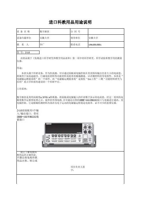
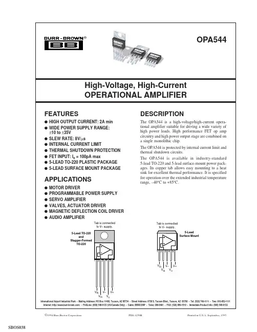
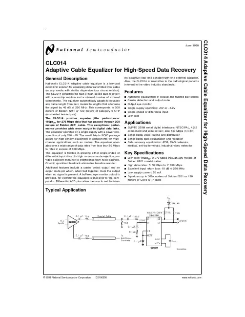
CLC014Adaptive Cable Equalizer for High-Speed Data RecoveryGeneral DescriptionNational’s CLC014adaptive cable equalizer is a low-cost monolithic solution for equalizing data transmitted over cable (or any media with similar dispersive loss characteristics).The CLC014simplifies the task of high-speed data recovery with a one-chip solution and a minimal number of external components.The equalizer automatically adapts to equalize any cable length from zero meters to lengths that attenuate the signal by 40dB at 200MHz.This corresponds to 300meters of Belden 8281or 120meters of Category 5UTP (unshielded twisted pair).The CLC014provides superior jitter performance:180ps pp for 270Mbps data that has passed through 200meters of Belden 8281cable.This exceptional perfor-mance provides wide error margin in digital data links.The equalizer operates on a single supply with a power con-sumption of only 290mW.The small 14-pin SOIC package allows for high-density placement of components for multi-channel applications such as routers.The equalizer oper-ates over a wide range of data rates from less than 50Mbps to rates in excess of 650Mbps.The equalizer is flexible in allowing either single-ended or differential input drive.Its high common mode rejection pro-vides excellent immunity to interference from noise sources.On-chip quantized feedback eliminates baseline wander.Additional features include a carrier detect output and an output mute pin which,when tied together,mute the output when no signal is present.A buffered eye monitor output is provided,for viewing the equalized signal prior to the com-parator.Differential AEC pins allow the user to set the inter-nal adaptive loop time constant with one external capacitor.Also,the CLC014is insensitive to the pathological patterns inherent in the video industry standards.Featuresn Automatic equalization of coaxial and twisted pair cables n Carrier detection and output mute n Output eye monitorn Single supply operation:+5V or −5.2V n Single-ended or differential input nLow costApplicationsn SMPTE 259M serial digital interfaces:NTSC/PAL,4:2:2component and wide screen;also 540Mbps (4:4:4:4)n Serial digital video routing and distribution n Serial digital data equalization and reception n Data recovery equalization:ATM,CAD networks,medical,set top terminals,industrial video networksKey Specificationsn Low jitter:180ps pp @270Mbps through 200meters of Belden 8281coaxial cablen High data rates:<50Mbps to >650Mbps n Excellent input return loss:19dB @270MHz n Low supply current:58mAn Equalizes up to 300+meters of Belden 8281or 120meters of Cat 5UTP cableTypical ApplicationDS100056-4June 1998CLC014Adaptive Cable Equalizer for High-Speed Data Recovery©1999National Semiconductor Corporation Connection DiagramVertical scale: 200mV/div270Mbps data through 300m of Belden 8281 coax cableDS100056-2Vertical scale: 200mV/div270Mbps data through 300m of Belden 8281 coax cableDS100056-3DS100056-114-Pin SOICOrder Number CLC014AJE See NS Package Number M14A 2Absolute Maximum Ratings(Note1)If Military/Aerospace specified devices are required, please contact the National Semiconductor Sales Office/ Distributors for availability and specifications.Supply Voltage(V CC–V EE)−0.3V,+6.5V Maximum Junction Temperature+150˚C Storage Temperature Range−65˚C to+150˚C Lead Temperature(Soldering4sec.)+260˚C ESD Rating(Note14)<500V θJA14-Pin SOIC(AJE)95˚C/W MTTF(based on limited life test data) 4.8x10⁷hours Recommended Operating ConditionsSupply Voltage(V CC–V EE) 4.5V to5.5V Operating Temperature Range−40˚C to+85˚C Series Input Resistance(In Series w/DI&DI)100ΩInput Coupling Capacitance0.1µF AEC Capacitor(Connectedbetween AEC+&AEC−)50pF to1µF Cable Input Voltage Swing(Note4)720to880mV pp DO/DO Minimum Voltage(Note15)V CC–1.6VElectrical Characteristics(V CC=+5V,V EE=0V,signal source swing=0.8V pp(Note4),C AEC=100pF)Parameter ConditionsTyp+25˚CMin/Max+25˚CMin/Max−40˚C to+85˚CUnitsDYNAMIC PERFORMANCEResidual Jitter100meters Belden8281270Mbps PRN(Note5)150250400ps pp 200meters Belden8281270Mbps PRN(Note5)180250400ps pp 300meters Belden8281270Mbps PRN(Notes3,5)350500750ps pp Equalization Time Constant100meters Belden8281C AEC=100pF(Note6) 1.5__µs200meters Belden8281C AEC=100pF(Note6) 2.0__µs300meters Belden8281C AEC=100pF(Note6) 3.2__µs output rise and fall time(20%–80%)R collector=75Ω750__ps output duty cycle distortion30__ps minimum average transition density1/50__trans/ns maximum average data rate150m Belden8281(Note7)650__MbpsV CC Jitter Sensitivity27MHz0.85__ns/V 270MHz 1.90__ns/VV EE Jitter Sensitivity27MHz0.55__ns/V 270MHz 1.45__ns/V STATIC PERFORMANCESupply Current(Includes Output Current)V AEC=0V(Note3)5848/6840/75mAV AEC=0.4V(Note3)5343/6437/70mA Input and Output ParametersDO/DO output current108.7/11.38.0/12mADO/DO output voltage swing R collector=75Ω(Note3)750650/850600/900mVDI/DI common mode voltage 3.4__VAEC differential voltage Belden8281 1.5__mV/meter AEC+/AEC−common mode 3.6__V output eye monitor(OEM)bias potential 3.2__V carrier detect(CD)current output-HIGH CD V OH=4.5V−400__µA carrier detect(CD)current output-LOW CD V OL=0.5V600__µA MUTE voltage input-HIGH(Note3) 1.8 2.0 2.0V MUTE voltage input-LOW(Note3) 1.20.80.8V3Electrical Characteristics(Continued)(VCC=+5V,V EE=0V,signal source swing=0.8V pp(Note4),C AEC=100pF)Parameter ConditionsTyp+25˚CMin/Max+25˚CMin/Max−40˚C to+85˚CUnitsInput and Output ParametersMUTE current input-HIGH V IH=5V(Note3) 5.0±100±500nA MUTE current input-LOW V IL=0V(Note3)0.2±100±500nA TIMING PERFORMANCECD Response Timecarrier applied(Note8) 1.0__µs carrier removed(Note9)12__µs MUTE response time(Note10) 2.0__ns MISCELLANEOUS PERFORMANCEinput resistance single-ended7.3__kΩinput capacitance single-ended(Note11) 1.0__pF input return loss@270MHz Z o=75Ω(Note12)19__dB maximum cable attenuation200MHz(Note13)40__dB Note1:“Absolute Maximum Ratings”are those values beyond which the safety of the device cannot be guaranteed.They are not meant to imply that the devices should be operated at these limits.The table of“Electrical Characteristics”specifies conditions of device operation.Note2:Min/max ratings are based on product characterization and simulation.Individual parameters are tested as noted.Outgoing quality levels are determined from tested parameters.Note3:J-level:spec.is100%tested at+25˚C.Note4:These specifications assume an800mV pp signal at the cable input.Levels above and below800mV are allowable,but performance may vary.The cable will attenuate the signal prior to entering the equalizer.Note5:Peak-to-peak jitter is defined as6times the rms jitter.Note6:For more information,see“CLC014Operation”and“Design Guidelines”.Note7:50%eye opening.Note8:Time from application of a valid signal to when the CD output asserts high.Note9:Time from the removal of a valid signal to when the CD output asserts low.Note10:Time from assertion of MUTE to when the output responds.Note11:Device only.Does not include typical pc board parasitics.Note12:Includes typical pc board parasitics.Note13:This sets the maximum cable length for the equalizer.Note14:Human body model,1.5kΩin series with100pF;based on limited test data.Note15:To maintain specified performance,do not reduce DO/DO below this level.4Time (1ns/div)Data Rate: 270MbpsDS100056-5Time (1ns/div)Data Rate: 270MbpsDS100056-8Before Equalization:200m of Belden 8281 Coaxial CableTime (1ns/div)Data Rate: 270MbpsDS100056-6After Equalization:200m of Belden 8281 Coaxial CableTime (1ns/div)Data Rate: 270MbpsDS100056-9Before Equalization:300m of Belden 8281 Coaxial CableTime (1ns/div)Data Rate: 270MbpsDS100056-7After Equalization:300m of Belden 8281 Coaxial CableTime (1ns/div)Data Rate: 270MbpsDS100056-10 5Time (6ns/div)Data Rate: 51.7MbpsDS100056-11Time (6ns/div)Data Rate: 51.7MbpsDS100056-14Before Equalization:100m Category 5 UTP at 155MbpsTime (2ns/div)Data Rate: 155MbpsDS100056-12After Equalization:100m Category 5 UTP at 155MbpsTime (2ns/div)Data Rate: 155MbpsDS100056-15Before Equalization:100m Category 5 UTP at 311MbpsTime (1ns/div)Data Rate: 311MbpsDS100056-13After Equalization:100m Category 5 UTP at 311MbpsTime (1ns/div)Data Rate: 311MbpsDS100056-1667Pin DefinitionsName Pin #DescriptionDI,DI 8,9Differential data inputs.DO,DO 13,14Differential collector data outputs (ECL compatible).AEC+,AEC−6,7AEC loop filter pins.A capacitor connectedbetween these pins governs the loop response for the adaptive equalization loop.OEM3Eye monitor output.The output of the equalization filter.CD 5Carrier detect.(Low when no signal is present).MUTE12Output MUTE.(Active low.)Carrier detect may be tied to this pin to inhibit the output when no signal is present.V CC 1,2,4Positive supply pins (ground or +5V).V EE10,11Negative supply pins (−5.2V or ground).OperationThe CLC014Adaptive Cable Equalizer provides a complete solution for equalizing high-bit-rate digital data transmitted over long transmission lines.The following sections furnish design and application information to assist in completing a successful design:•Block diagram explanation of the CLC014•Recommended standard input and output interface con-nections•Common applications for the CLC014•Measurement,PC layout,and cable emulation boxes For applications assistance in the U.S.,call 800-272-9959to contact a technical staff member.BLOCK DESCRIPTIONThe CLC014is an adaptive equalizer that reconstructs serial digital data received from transmission lines such as coaxial cable or twisted pair.Its transfer function approximates the reciprocal of the cable loss characteristic.The block diagram in Figure 2depicts the main signal conditioning blocks for equalizing digital data at the receiving end of a cable.The CLC014receives baseband differential or single-ended digi-tal signals at its inputs DI and DI.The Equalizer block is a two-stage adaptive filter.This filter is capable of equalizing cable lengths from zero meters to lengths that require 40dB of boost at 200MHz.The Quantized Feedback Comparator block receives the differential signals from the equalizer filter block.This block includes two comparators.The first comparator incorporates a self-biasing DC restore circuit.This is followed by a second high-speed comparator with output mute capability.The sec-ond comparator receives and slices the DC-restored data.Its outputs DO and DO are taken from the collectors of the output transistors.MUTE latches DO and DO when a TTL logic low level is applied.The Adaptive Servo Control block produces the signal for controlling the filter block,and outputs a voltage proportional to cable length.It receives differential signals from the output of the filter block and from the quantized-feedback compara-tor (QFBC)to develop the control signal.The servo loop re-sponse is controlled by an external capacitor placed across the AEC+and AEC−pins.Its output voltage,as measured differentially across AEC+and AEC−,is roughly proportional to the length of the transmission line.For Belden 8281co-axial cable this differential voltage is about 1.5mV/meter.Once this voltage exceeds 500mV,no additional equaliza-tion is provided.The Carrier Detect (CD)block monitors the signal power out of the equalizing filter and compares it to an internal refer-ence to determine if a valid signal is present.A CMOS high output indicates that data is present.The output of CD can be connected to the MUTE input to automatically latch the outputs (DO and DO),preventing random transitions when no data is present.The Output Eye Monitor (OEM)provides a single-ended buffered output for observing the equalized eye pattern.The OEM output is a low impedance high-speed voltage driver capable of driving an AC-coupled 100Ωload.DS100056-20FIGURE 1.CLC014Equalizer Application CircuitDS100056-21FIGURE 2.CLC014Block Diagram8Input InterfacingThe CLC014accepts either differential or single-ended input voltage specified in Static Performance .The following sec-tions show several suggestions for interfaces for the inputs and outputs of the CLC014.SINGLE-ENDED INPUT INTERFACE:75ΩCoaxial Cable The input is connected single-ended to either DI or DI as shown in Figure 3.Balancing unused inputs helps to lessen the effects of e the equivalent termination of 37.5Ωto balance the input impedance seen by each pin.It also helps to terminate grounds at a common point.Resistors R x and R y are recommended for optimum performance.The equalizer inputs are self-biasing.Signals should be AC coupled to the inputs as shown in Figure 3.DIFFERENTIAL INPUT INTERFACE:Twisted Pair A recommended differential input interface is shown in Fig-ure 4.Proper voltage levels must be furnished to the input pins and the proper cable terminating impedance must be provided.For Category 5UTP this is approximately 100Ω.Figure 4shows a generalized network which may be used to receive data over a twisted pair.Resistors R 1and R 2provide the proper terminating impedance and signal level adjust-ment.The blocking capacitors provide AC coupling of the at-tenuated signal levels.The plots in the Typical Perfor-mance Characteristics section demonstrate various equalized data rates using Category 5UTP at 100meter lengths.A full schematic of a recommended driver and re-ceiver circuit for 100ΩCategory 5UTP is provided in the Typical Applications section with further explanation.Output InterfacingThe outputs DO and DO produce ECL logic levels when the recommended output termination networks are used.TheDO and DO pins are not complementary emitter coupled logic outputs.Instead,the outputs are taken off of the collec-tors of the transistors.Therefore,care must be taken to meet the interface threshold levels required by ECL families.Rec-ommended interfaces for standard ECL families are shown in the following circuits.DIFFERENTIAL LOAD-TERMINATED OUTPUT INTERFACEFigure 5shows a recommended circuit for implementing a differential output that is terminated at the load.A diode or 75Ωresistor provides a voltage drop from the positive supply (+5V for PECL or Ground for ECL operation)to establish proper ECL levels.The resistors terminate the cable to the characteristic impedance.The output voltage swing is deter-mined by the CLC014output current (10mA)times the ter-mination resistor.For the circuit in Figure 5,the nominal out-put voltage swing is 750mV.DIFFERENTIAL SOURCE-TERMINATED OUTPUT INTERFACEFigure 6is similar to Figure 5except that the termination is provided at the source.This configuration may also be used for single-ended applications.However,the unused output must still be terminated as shown.TERMINATING PHYSICALLY SEPARATED OUTPUTS When the two outputs must be routed to physically separate locations,the circuit in Figure 6may be applied.Alterna-tively,if load termination is desired,the circuit in Figure 7DS100056-22FIGURE 3.Single-Ended 75ΩCable Input Interface DS100056-24FIGURE 4.Twisted Pair Input InterfaceDS100056-25FIGURE 5.Differential Load TerminatedOutput InterfaceDS100056-26FIGURE 6.Differential Source TerminatedOutput Interface9Output Interfacing(Continued)may be used.The resistive divider network provides75Ωter-mination and establishes proper ECL levels.This circuit con-sumes slightly more power than the previous circuits.Design GuidelinesSELECTING THE AUTOMATIC EQUALIZER CAPACITOR The AEC capacitor sets the loop time constantτfor the equalizer’s adaptive loop response time.The following for-mula is used to set the loop time constant:τ=R•C AEC•10−6R is a conversion factor that is set by internal equalizer pa-rameters and cable length.For Belden8281coaxial cable, the R values are(τ=µs,C AEC in pF):CableLengthR Value(Ohms)100meters15000200meters20000300meters32000For example,a C AEC value of100pF results in an adaptive loop time constant of2µs at200meters of cable. CONNECTION AND OPERATION OF CD AND MUTE Carrier Detect(CD)is a CMOS output that indicates the presence of equalized data from the filter.This CD output can be connected to MUTE to suspend changes in the data outputs DO and DO,if no valid signal exists.This simple configuration prevents random output transitions due to noise.For sparse transition patterns it is recommended that a capacitor be connected to CD as shown in Figure1.Add a capacitor to pin5to slow the response time of Carrier Detect when Carrier Detect is connected to MUTE.The ca-pacitor reduces sensitivity to pathological patterns.Patho-logical patterns are defined as sparse data sequences with few transitions.OUTPUT EYE MONITOR OEM CONNECTIONSThe OEM is a high-speed,buffered output for monitoring the equalized eye pattern prior to the output comparator.Its out-put is designed to drive an AC-coupled50Ωcoaxial cable with a series50Ωbackmatch resistor.The cable should be terminated with50Ωat the oscilloscope.Figure1shows a schematic with a typical connection.MINIMUM DATA TRANSITIONSThe CLC014specifies a minimum transition rate.For the CLC014this sets the minimum data rate for transmitting data through any cable medium.The CLC014minimum average transition density is found in the Electrical Characteristics section of the datasheet.POWER SUPPLY OPERATION AND THERMAL CONSIDERATIONSThe CLC014operates from either+5V or−5.2V single sup-plies.Refer to Figure1when operating the part from+5V. When operating with a−5.2V supply,the V EE pins should be bypassed to ground.The evaluation board and associated literature provide for operation from either supply. Maximum power dissipation occurs at minimum cable length.Under that condition,I CC=58mA.Total power dissipated:P T=(58mA)(5V)=290mWPower in the load:P L=(0.7V)(11mA)+(37.5)(11mA)2=12mW Maximum power dissipated on the die:P DMAX=P T–P L=278mWJunction Temperature=(θJA)(278mW)+T A=T A+26˚CDS100056-27FIGURE7.Alternative Load TerminatedOutput Interface10Layout and MeasurementThe printed circuit board layout for the CLC014requires proper high-speed layout to achieve the performance speci-fications found in the datasheet.The following list contains a few rules to follow:e a ground plane.2.Decouple power pins with 0.1µF capacitors placed≤0.1”(3mm)from the power pins.3.Design transmission strip lines from the CLC014’s input and output pins to the board connectors.4.Route outputs away from inputs.5.Keep ground plane ≥0.025”(0.06mm)away from the in-put and output pads.Figure 8shows a block level measurement diagram,while Figure 15on depicts a detailed schematic.A pseudo-random pattern generator with low output jitter was used to provide a NRZI pattern to create the eye diagrams shown in the Typi-cal Performance Characteristics section.Since most pattern generators have a 50Ωoutput imped-ance,a translation can be accomplished using a CLC006Cable Driver as an impedance transformer.A wide band-width oscilloscope is needed to observe the high data rate eye pattern.When monitoring a single output that is termi-nated at both the equalizer output and the oscilloscope,the effective output load is 37.5Ω.Consequently,the signal swing is half that observed for a single-ended 75Ωtermination.Troubleshooting with scope probes can affect the equaliza-tion.For high data rates,use a low capacitance probe with less than 2pF probe capacitance.Evaluation boards and lit-erature are available for quick prototyping and evaluation of the CLC014Adaptive Cable Equalizer.The CLC014con-tains CMOS devices and operators should use grounding straps when handling the parts.Figure 9shows the CLC014’s internal power supply routing.Bypass V CC (pin 4)by:•Monolithic capacitor of about 0.1µF placed less than 0.1”(3mm)from the pin•Tantalum capacitor of about 6.8µF for large current sig-nal swings placed as close as convenient to the CLC014To minimize ringing at the CLC014’s inputs,place a 100Ωre-sistor in series with the input.This resistor reduces induc-tance effects.Several layout techniques can improve high speed perfor-mance:•Keep input,output and AEC traces well separated •Use balanced input termination’s•Avoid routing traces close to the CLC014’s input traceDS100056-28FIGURE 8.Typical Measurement BlockDS100056-29FIGURE 9.Power Package Routing Fixture11Layout and Measurement(Continued)•Maintain common return points for components •Use guard tracesThe input lines of the CLC014use a 100Ωseries resistors at the input pins.This decreases the inductive effects internal to the part to reduce ringing on fast rise and fall times.Refer to the evaluation board layout for further suggestions on lay-out for the CLC014Adaptive Equalizer.EQUALIZATION CURVEThe CLC014Adaptive Cable Equalizer has a maximum equalization response as shown in Figure 10.This response may be obtained by forcing >0.5V differentially at the AEC pins.CABLE EMULATION BOXESSome cable emulation boxes will not mimic cables correctly.When evaluating the CLC014,it is strongly recommended that actual cable be used to determine the various perfor-mance parameters.Typical ApplicationsCOAXIAL CABLE RECEIVER (Page 1)The CLC014equalizer application shown on page 1will equalize a variety of coaxial cables up to lengths that attenu-ate the signal by 40dB at 200MHz.The application shows the proper connection for a single cable driven with a CLC006driver.Carrier Detect (CD)is connected to MUTE to latch outputs DO and DO in the absence of an input signal to the equalizer.Refer to the CLC014’s evaluation board layout for additional suggestions.National can supply most of the major components required to design a transmission line repeater.Figure 11shows a typical repeater design using the CLC006,CLC014,and the CLC016.The design functions supported by each chip are:CLC006:Cable connection chipBoosts drive for transmission to next repeater or final destinationsCLC014:Receive serialized digital data from incomingtransmission linesEqualizes the incoming data CLC016:Retimes the equalized data (improving jitter)The CLC016is a multi-rate data retiming PLL.The circuit (Figure 11)will work at up to 4different data rates with no ad-ditional components or manual tuning.M a g n i t u d e (5d B /d i v )Frequency (Hz)10k100k 1M 10M 100M 1GDS100056-30FIGURE 10.Maximum Equalization Response 12Typical Applications(Continued)DIGITAL VIDEO (SDV)ROUTERSThe CLC014provides performance that complies with the SMPTE 259M standard for serial digital video (SDV)trans-mission over coaxial cable.One common application is in SDV routers,which provide a switching matrix for connecting video source equipment (e.g.,cameras)to destination equip-ment (e.g.,video tape recorders,monitors,etc.).Figure 12shows a typical configuration for an SDV router,in-cluding equalizers,a crosspoint switch,data retimers,and cable drivers.The CLC014is used in its standard configura-tion in this application,and automatically equalizes cable lengths from zero meters to greater than 300meters at 360MHz (see plots in Typical Performance Characteris-tics section).The equalized outputs are connected to the dif-ferential inputs of the crosspoint switch.The CLC016Data Retimer receives the data from the crosspoint and performs the clock and data recovery functions,further reducing jitter.Finally,the retimed data is driven into the coaxial cable by a CLC006Cable Driver (with two amplitude-adjustable out-puts)or a CLC007Cable Driver (with four outputs).TWISTED PAIR DRIVERA low-cost medium for transmitting data is twisted pair.Cat-egory 5UTP has an attenuation characteristic similar to Belden 8281coaxial cable but scaled in length:120meters of Category 5UTP is roughly equivalent to 300meters of Belden 8281cable.When properly implemented,the CLC014will equalize data rates up to 625Mbps over Cat-egory 5UTP .The maximum data rate depends upon the cable length.A plot of Maximum Data Rate vs Cable Length is found in the Typical Performance Characteristics sec-tion for Belden 8281,and can be scaled as stated above to estimate maximum cable lengths and data rates for UTP .Category 5UTP has a characteristic impedance of approxi-mately 100Ω.The CLC006in Figure 13is used to drive the twisted pair AC-coupled with a series 0.1µF capacitor and a 50Ωresistor in each differential output.The CLC014Adap-tive Equalizer requires 800mV pp from the transmit side ofDS100056-31FIGURE 11.Typical Repeater DesignDS100056-32FIGURE 12.Video Routing Block Diagram13DS100056-33FIGURE 13.Twisted Pair EqualizationDS100056-34FIGURE 14.Before and After Equalization at 622MbpsThrough 50Meters of Category 5UTP100Ω37.5Ω0.1µMUTEC AECDI DICD DO DOAEC+AEC-100Ω75ΩCLC014Adaptive Cable Equalizer75Ω Coax Cable0.1µV cc75Ω75Ω1N41480.1µ0.1µF43.3Ω86Ω50 – 75Ωminimum loss pad270Mbps data through 300m of Belden 8281 coax cable800mV pp 1ns/divCan substitute a 75Ω resistorVertical scale: 200mV/divEnd of cable before equalization1ns/divVertical scale: 200mV/divEnd of cable afterequalizationDisplayCSA907TPattern 223-1Tektronix DataCLK Output CSA907T 1.3V ppDS100056-35FIGURE 15.Typical Measurement Setup 14Evaluation BoardAn evaluation board layout and schematic are shown on the following pages.The artwork shows the board solder masks, trace layers,and ground plane.To order an evaluation board contact your local sales representative or National support center and request part number CLC730063.The evaluation board provides an LED and switches to oper-ate the CLC014in various modes of operation.The power supplies,which must be correctly connected and jumpered for positive or negative voltage operation,are identified on the printed board silk screen.Insert all tantalum capacitors as shown in the schematic or silk screen.A complete bill of materials is given in the accompanying table.The compo-nents recommended in the materials list are SMPTE259M standard.DS100056-36FIGURE16.Evaluation Board Schematic 15Evaluation Board(Continued)CLC014Equalizer Evaluation BoardItem ReferenceDesignatorDescription Quantity1Q12N3904transistor1 2CR11N4148switching diode1 3J1,J2,J3,J4,J5receptacle vertical BNC PC Amphenol#31-5329-52RFX5 4J6banana jack,black,EF Johnson#108-0903-0011 5J7banana jack,red,EF Johnson#108-0902-0011 6R6,R710kΩ,1/8W,1206,1%chip resistors2 7R8,R9,R10,R1175Ω,1/8W,1206,1%chip resistors4 8R13 1.33kΩ,1/8W,1206,1%chip resistors1 9R3,R410Ω,1/8W,1206,1%chip resistors2 10R1,R2100Ω,1/8W,1206,1%chip resistors2 11R1420kΩ,1/8W,1206,1%chip resistors1 12R122kΩ,1/8W,1206,1%chip resistors1 13R549.9Ω,1/8W,1206,1%chip resistors1 14C2,C3,C9,C120.01µFd,10%X7R surface mount cap3 15C4,C7,C8,C10,C110.1µFd,10%X7R surface mount cap5 16C1100pFd,5%NPO surface mount cap1 17C5,C6 6.8µFd,16V tantalum capacitor2 18CLC730063printed circuit board1 19U1CLC014AJE1 20D1LED,GENERAL PURPOSE1LAYOUTThe CLC014requires proper high-speed layout techniquesto obtain best results.A few recommended layout rules to fol-low for best results when using the CLC014Adaptive CableEqualizer are:e a ground plane.2.Decouple power pins with0.01µF capacitors placed≤0.1”(3mm)from the power pins.3.Design transmission lines to the inputs and outputs.4.Route outputs away from inputs.5.Remove ground plane≥0.025”(0.06mm)from the inputand output pads.The solder masks with component locations,trace layer,andground plane board layer are shown next.16。