YAGEO贴片电容规格书
- 格式:pdf
- 大小:219.18 KB
- 文档页数:11
【 南京南山半导体有限公司 — 贴片电容选型资料】MULTILAYER CHIP CERAMIC CAPACITORCOG/COHCOG, ,-55125,030ppm/060ppm/0805CG101J500NT(PF) ( 0402 0.04 0603 0.06 0805 0.08 1206 0.12 ) 0.02 0.03 0.05 0.06 1.00 1.60 2.00 3.20 ( ) 0.50 0.80 1.25 1.60 CG CH COG NPO COH 100 101 102 10 100 1J G C B D5.00% 2.00% 0.25PF 0.10PF 0.50PF10 10 10 1026R3 100 250 5006.3V 10V 25V 50VS C N / / T BWBWTL mm L 0402 0603 0805 1206 1005 1608 2012 3216 1.00 1.60 2.00 3.20 0.05 0.10 0.20 0.30 W 0.50 0.80 1.25 1.60 0.05 0.50 0.10 0.80 0.20 0.80 1.00 1.25 0.20 0.80 1.00 1.25 T WB 0.05 0.25 0.10 0.30 0.20 0.50 0.20 0.20 0.20 0.60 0.20 0.20 0.10 0.10 0.20 0.3015【 南京南山半导体有限公司 — 贴片电容选型资料】0.80 0.20 1.00 0.20 0.50 0.80 0.20 1.00 0.20 0.600.20 0.30【 南京南山半导体有限公司 — 贴片电容选型资料】MULTILAYER CHIP CERAMIC CAPACITORCOG/COH 0402 0603 0805 12066.3V 10V 16V 25V 50V 6.3V 10V 16V 25V 50V 6.3V 10V 16V 25V 50V 6.3V 10V 16V 25V 50V0.5PF 1PF 2PF 3PF 4PF 5PF 6PF 7PF 10PF 22PF 33PF 47PF 68PF 100PF 120PF 150PF 180PF 220PF 330PF 470PF 560PF 680PF 1000PF 2200PF 2700PF 3300PF 4700PF 5600PF 6800PF 10nF 12nF 15nF 22nF 47nF 68nF 100nF17【 南京南山半导体有限公司 — 贴片电容选型资料】04020603080512066.3V 10V 16V 25V 50V 6.3V 10V 16V 25V 50V 6.3V 10V 16V 25V 50V 6.3V 10V 16V 25V 50VCapacitance0.5PF 1PF 2PF 3PF 4PF 5PF 6PF 7PF 10PF 22PF 33PF 47PF 68PF 100PF 120PF 150PF 180PF 220PF 330PF 470PF 560PF 680PF 1000PF 2200PF 2700PF 3300PF 4700PF 5600PF 6800PF 10nF 12nF 15nF 22nF 47nF 68nF 100nF【 南京南山半导体有限公司 — 贴片电容选型资料】MULTILAYER CHIP CERAMIC CAPACITORCOG COHPH~SLCOG PH SH SL TH RH UJCOH1-55125-55851. 2. 3. 2 4. 5. , , , , , 103 4 Cr 5PF 0.56% -4 5PF Cr 50PF 1.5 [(150/Cr)+7] 10 Cr 50PF 0.15% C C 10nF Ri 10nF Ri 5 10 Cr 500s 3 50mA 150+0/-10 8 25 9 75 235 5 2 0.5 25 60 265 10 1 25 : 1 2 100 170 120 200 1 1 2.5mm/ 24 2 5 5 5 2.5mm/ 245 24 -55 125 2 -55 85 60 510:HP4278A 1. 2. 3. (D.F.) :1.0 C : : (HP4284 25 5 0.2V 0.1MHz; 0.1KHZ ) 1000PF,1.0 :SF2511 , 60 60 1 5 :30% 75%5:C<1000PF,1.06I.R.7>3x150+0/-10 5% 0.5PF D.F. 10 I.R. 24 245【 南京南山半导体有限公司 — 贴片电容选型资料】General COGCOHPHSL MLCC reliability test methodStandard Number Item COG COH MLCC for General-use -55 125 PH, RH, SH, TH, UJ, SL MLCC for General-use -55 85 Check by using microscope 10 . Test Method1Operating Temperature RangeAppearance21.Good ceramic body color continuity. 2.The chips have no visual damages and must be very smooth. 3.No exposed inner- electrode, no cracks or holes. 4.The outer electrode should have no cracks, holes, damages or surface oxidation. 5.Outer electrode no prolongation or the prolongation is less than half of that of the termination width.3 4 5Dimensions Capacitance Dissipation Factor (DF)Within the specified dimensions Within the specified tolerance Cr 5PF 0.56% 5PF Cr 50PF 1.5 [(150/Cr)+7] 10-4 Cr 50PF 0.15% C C 10nF Ri 10nF Ri 5 1010 Cr 500sUsing micrometer or vernier calipers Measuring Equipments:HP4278 capacitance meter,HP4284 capacitance, Measuring Conditions: 1.Measuring Temperature:25 5 .Humidity: 30% 75%. 2.Measuring Voltage:1.0 0.2V. 3.Measuring Frequency:C<1000PF 1.0 0.1MHz C 1000PF 1.0 0.1KHz Measuring Equipment:Insulation resistance meter (such as Sf2511 insulation resistance). Measuring Method:Must measure at rated voltage, and measure the IR within 60 5 seconds. Must measure at 3 times rated voltage, dwell time: 60 1 seconds, no short and the changing/discharging current less than 50mA. First, pre-heat: heat treat 60 5 minutes at 150+0/-10 , then set it for 24 2 hours at room temperature. Measure the capacitance at -55 125 or -55 85 , the capacitance change ratio comparing to that of 25 must be within the specified range. Dip the capacitor into ethanol or colophony solution, and then dip it into 235 5 ( or 245 5 leadless eutedtic solder solution ) eutectic solder solution hanving lead for 2 0.5 seconds. Dipping speed: 25 2.5mm/second. First pre-heat: heat treat for 60 5 minutes at 150+0/-10 , then set it for 24 2 hours at room temperature. Then pre-heat the capacitance according to the following chart. Dip the capacitor into 265 5 eutectic solder solution for 10 1 seconds. Then set it for 24 2 hours at room temperature, then measure. Dipping speed: 25 2.5mm/second. Preheat conditions: Stage 1 2 Temperature 100 170 120 200 Time 1minute 1minute6Insulation Resistance7Withstanding Voltage Capacitance Temperature Characteristic>3x rated continuous working voltage Must meet the capacitor character temperature coefficient requirements within the operating temperature range. Tin coverage should be 75% of the outer electrode Appearance Cap. Change ratio DF No defects visible 5%or 0.5PF (whichever is larger)89SolderabilityResistance to Soldering10Same as original spec Same as original specIR46【 南京南山半导体有限公司 — 贴片电容选型资料】MULTILAYER CHIP CERAMIC CAPACITOR1 10N11 10N,10 1 :1.0mm/ 11.5mm 10 D.F. 12 55Hz 210 55Hz 10Hz 6 123 420 mm mmmm13mmmmmmmm150+0/-10 14 24 2 24 260 547【 南京南山半导体有限公司 — 贴片电容选型资料】NumberItems Adhesive Strength of TerminationStandard No removal of the terminations or other defect shall occurTest Method Solder the capacitor to the test jig (glass epoxy resin board) shown in Fig.1 using a eutectic solder.Then apply a 10N force inthe direction shown as the arrowhead.The aoldering shall be done either with an iron or using the reflow method and shall be conducted with care so that an iron or using the refow method and shall be conducted with care so that the soldering is uniform and free of defects such as heat shock,etc. 10N,10 1s Speed:1.0mm/s Glss epoxy resinboard11Fig.1 Vibration Resistance Appearance Capacitance No defects or abnormities Within the specified tolerance range Same as original spec12DFSolder the capacitor to the test jig (glass epoxy resin board). The capacitor should be subjected to a simple harmonic motion having a total amplitude of 1.5mm, the frequency being varied uniformly between the approximate limits of 10 and 55Hz, shall be traversed (from 10 Hz to 55 Hz then 10 Hz again) in approximately 1 minute.This motion shall be applied for a period of 2 hours in each 3 mutually perpendicular directions (total is 6 hours).Same i standarFif.2 Bending Resistance No cracks or other defects shall occur Solder the capacitor to the test jig (glass epoxy resin board) shown in Fig.3 using a eutectic solder. Then apply a 10N force in the direction shown as Fig.4. The soldering shall be done either with an iron or using the reflow method and shall be conducted with care so that the soldering is uniform and free of defects such as mm heat shock, etc.mm13mm mm mm14Temperature CycleAppearance No defects or abnormitiesPre-treatment: Heat-treat the capacitor for 60 5minutes at 150+0/-10 , then set it for 24 2 hours at room temperature. Perform five cycles according to the four heat treatments listed in the following table. Set it for 24 2 hours at room temperature, then measure.48mm【 南京南山半导体有限公司 — 贴片电容选型资料】MULTILAYER CHIP CERAMIC CAPACITOR2.5% 0.25PF, 1 10000M 2 3 4 2 3 30 3 2 3 30 3 2 314D.F. I.R.40 290 95 24 2500+24/-05% 0.5PF, 15 ( ) D.F. I.R. 10000M40 2 500+24/-0 5% 0.5PF, 16 D.F. I.R. 10000M90 95 24 22 50mA 5% 0.5PF, 17 D.F. I.R. 10000M1000 12 24 249【 南京南山半导体有限公司 — 贴片电容选型资料】NumberItem Temperature CycleStandard Cap. Change ratio D.F. I.R. 2.5% or 0.25 PF (whichever is larger) Same as original spec More than 10000M Heat-treatment:Test Method14stage temperature 1 lowest opeating temperature 3 2 normal temperature 3 high operating temperature 2 4 normal temperaturetime min. 30 3 2 3 30 3 2 3Humidity Steady StateAppearance Cap. Change ratio D.F. I.R.No defects or abnormities 5% or 0.5 PF (whichever is larger) Same as original spec More than 10000MSet the capacitor for 500+24/-0 hours at the condition of 40 2 and 90-95% humidity. Then remove and set it for 24 2 hours at room temperature, then measure.15Humidity LoadAppearance Cap. Change ratioNo defects or abnormities 5% or 0.5 PF (whichever is larger) Same as original spec More than 10000MApply rated voltage to the capacitor for 500+24/-0 hours at the condition of 40 2 and 90-95% humidity. Remove and set it for 24 2 hours at room temperature, then measure.16D.F. I.R.Life TestAppearance Cap. Change ratioNo defects or abnormities 5% or 0.5 PF (whichever is larger) Same as original spec More than 10000MApply two times rated voltage to the capacitor for 1000 12 hours at the upper temperature limits, the charging current should be less than 50mA. Remove and set it for 24 2 hours at room temperature, then measure.17D.F. I.R.5057-10%-5%0%5%10%COG 50VX7R 50V Z5U 50V Y5V50V010********-100%-80%-60%-40%-20%0%20%40%[Vdc]COG :1MHZ X7R,Z5U,Y5V:1KHZZ5U 50VY5V 50V X7R 50VC0G 50V0123-20%0%+20%+40%+60%^+80%COG PH RH SH TH UHCOG X7R Y5V,Z5U05010010001000010%0%-10%-20%-30%-40%[Hr]X7R20%0%[Vr ms ]COG :1MHZ X7R,Z5U,Y5V:1KHZMULTILAYER CHIP CERAMIC CAPACITOR58-5%0%5%10%-100%-80%-60%-40%-20%0%20%40%Z5U 50VY5V 50V X7R 50VC0G 50V0123-20%0%+20%+40%+60%^+80%COG X7R Y5V,Z5U05010010001000010%0%-10%-20%-30%-40%0%GENEREL-USE MLCC CHARCCTER PROFILESCapacitance change ratio DC Voltage[Vdc]Measuring condition COG :1MHzX7R,Z5U,Y5V:1KHzCOG and PHRH SH TH UH siriestemperature coefficentDC Capacitance-AC VoltageCharactericsCapacitance change_agingTime[Hr]X7R tempreture characteristicsZ5U [Vr ms ]Capacitance change ratioCapacitance change ratio Capacitance change ratio Capacitance change ratio。

P r o d u c t S p e c i f i c a t i o n –M a r c h 7, 2017 V .16DATA SHEETSURFACE-MOUNT CERAMIC MULTILAYER CAPACITORSGeneral purposeClass 1, NP016 V TO 50 V0.22 pF to 100 nFRoHS compliant & Halogen FreeSCOPEThis specification describes NP0 series chip capacitors with lead-free terminations. APPLICATIONS●Consumer electronics for example-Tuners-Television receivers-All types of cameras●Telecommunications●Data processing FEATURES●Supplied in tape on reel●Nickel-barrier end termination ●RoHS compliant●Halogen Free compliant ORDERING INFORMATION - GLOBAL PART NUMBER, PHYCOMP CTC & 12NCAll part numbers are identified by the series, size, tolerance, TC material, packing style, voltage, process code, termination and capacitance value.Y A G E O B R A N D o r d e r i n g c o d eGLOBAL PART NUMBER(PREFERRED)CC XXXX X X NPO X BN XXX(1) (2) (3) (4) (5)(1) SIZE – INCH BASED (METRIC)0201 (0603)0402 (1005)0603 (1608)0805 (2012)1206 (3216)1210 (3225)1812 (4532)(2) TOLERANCEB= ±0.1 pFC= ±0.25 pFD= ±0.5 pFF= ±1%G= ±2%J= ±5%K= ±10%(3) PACKING STYLER= Paper/PE taping reel; Reel 7 inchK= Blister taping reel; Reel 7 inchP= Paper/PE taping reel; Reel 13 inchF= Blister taping reel; Reel 13 inchC= Bulk case(4) RATED VOLTAGE7= 16 V8= 25 V9= 50 V(5) CAPACITANCE VALUE2 significant digits+number of zerosThe 3rd digit signifies the multiplying factor, and letter R is decimal pointExample: 121 = 12 x 101 = 120 pF0.6 ±0.03 0.3 ±0.03 Refer to table 2 to 50.10 0.20 0.20 0402 1.0 ±0.05 0.5 ±0.05 0.20 0.30 0.40 0603 1.6 ±0.10 0.8 ±0.10 0.200.60 0.40 0805 2.0 ±0.10 (1) 1.25 ±0.10 (1) 0.25 0.75 0.70 2.0 ±0.20 (2) 1.25 ±0.20 (2) 1206 3.2 ±0.15 (1) 1.6 ±0.15 (1) 0.25 0.75 1.40 3.2 ±0.30 (2) 1.6 ±0.20 (2) 1210 3.2 ±0.20 2.5 ±0.20 0.25 0.75 1.40 18124.5 ±0.203.2 ±0.200.250.752.20NOTE1. Dimension for size 0805 and 1206, C ≤ 1 nF2. Dimension for size 0805 and 1206, C > 1 nFDIMENSIONO U T L I N E SFig. 2 Surfacemounted multilayer ceramic c apacitor dimension CONSTRUCTION The capacitor consists of a rectangular block of ceramic dielectric in which a number of interleaved metal electrodes are contained. This structure gives rise to a high capacitance per unit volume.The inner electrodesare connected to the two end terminationsand finally covered with a layer of plated tin (NiSn). The terminations are lead-free.A cross section of the structure is shown in Fig.1.Surface mounted multilayer ceramic capacitor constructionC APACITANCE RANGE & THICKNESS FOR NP0CAPACITANCE RANGE & THICKNESS FOR NP0T able 3Sizes from 0201 to 0603 (continued)CAP.020*********25 V50 V16 V25 V50 V16 V25 V50 VNOTE1.Values in shaded cells indicate thickness class in mm2.Capacitance value of non E-12 series is on requestCAPACITANCE RANGE & THICKNESS FOR NP0T able 4Sizes from 0805 to 1812CAP.080512061210181216 V25 V50 V16 V25 V50 V25 V50 V 50 VNOTE1.Values in shaded cells indicate thickness class in mm2.Capacitance value of non E-12 series is on requestCAPACITANCE RANGE & THICKNESS FOR NP0T able 5Sizes from 0805 to 1812 (continued)CAP.080512061210181216 V25 V50 V16 V25 V50 V25 V50 V50 VNOTE1.Values in shaded cells indicate thickness class in mm2.Capacitance value of non E-12 series is on requestTHICKNESS CLASSES AND PACKING QUANTITYELECTRICAL CHARACTERISTICSN P0D I E L E C T R I C C A P A C I T O R S;N I S N T E R M I N A T I O N SUnless otherwise stated all electrical values apply at an ambient temperature of 20±1 °C, an atmospheric pressure of 86 to 106 kPa, and a relative humidity of 63 to 67%.DESCRIPTION VALUE Capacitance range 0.22 pF to 100 nF Capacitance toleranceC < 10 pF ±0.1 pF, ±0.25 pF, ±0.5 pFC ≥ 10 pF±1%, ±2%, ±5%, ±10% Dissipation factor (D.F.)C < 30 pF≤ 1 / ( 400 + 20C )C ≥ 30 pF≤ 0.1 % Insulation resistance after 1 minute at U r (DC) Rins≥ 10 GΩ or R ins × C r≥ 500 seconds whichever is less Maximum capacitance change as a function of temperature(temperature characteristic/coefficient):±30 ppm/°COperating temperature range: –55 °C to +125 °C T able 7Fig. 4 Typical capacitance change with respect tothe capacitance at 1 V as a function of DC voltage Fig. 3 Typical temperature coefficient as a function oftemperatureSample limits (broken lines).Requirement levels (dotted lines)Fig. 5 Typical tan δ as a function of temperature SOLDERING RECOMMENDATIONT able 8SOLDERING METHOD SIZE02010402060308051206≥ 1210Reflow Reflow only≥ 0.1 µF≥ 1.0 µF≥ 2.2 µF≥ 4.7 µF Reflow only Reflow/Wave--- < 0.1 µF< 1.0 µF< 2.2 µF< 4.7 µF---TESTS AND REQUIREMENTST able 9Test procedures and requirementsTEST TEST METHOD PROCEDURE REQUIREMENTSMounting IEC 60384-21/22 4.3The capacitors may be mounted on printed-circuit boardsor ceramic substratesNo visible damageVisualinspectionand dimension check4.4 Any applicable method using × 10 magnification In accordance with specificationCapacitance 4.5.1 Class 1:f = 1 MHz for C ≤ 1 nF, measuring at voltage 1 V rms at 20 °Cf = 1 KHz for C > 1 nF, measuring at voltage 1 V rms at 20 °CWithin specified toleranceDissipation factor (D.F.) 4.5.2 Class 1:f = 1 MHz for C ≤ 1 nF , measuring at voltage 1 V rms at 20 °Cf = 1 KHz for C > 1 nF, measuring at voltage 1 V rms at 20 °CIn accordance with specificationInsulationresistance4.5.3 At U r (DC) for 1 minute In accordance with specificationTemperature coefficient 4.6 Capacitance shall be measured by the steps shown in thefollowing table.The capacitance change should be measured after 5 min at eachspecified temperature stage.Temperature Coefficient shall be calculated from the formula asbelowTemp, Coefficient =610TxC1C1-C2Δ[ppm/℃]C1: Capacitance at step cC2: Capacitance at 125℃∆T: 100℃(=125℃-25℃)(2) Class IICapacitance Change shall be calculated from the formula asbelow∆C =C1C1-C2x 100%C1: Capacitance at step cC2: Capacitance at step b or d<General purpose series>Class1:∆ C/C: ±30ppmClass2:X7R: ∆ C/C: ±15%Y5V: ∆ C/C: 22~-82%<High Capacitance series>Class2:X7R/X5R: ∆ C/C: ±15%Y5V: ∆ C/C: 22~-82%TEST TEST METHOD PROCEDURE REQUIREMENTS4.7 A force applied for 10 seconds to the line joining theterminations and in a plane parallel to the substrate Forcesize ≥ 0603: 5N size = 0402: 2.5N size = 0201: 1NBond strength of plating on end face 4.8 Mounting in accordance with IEC 60384-22 paragraph 4.3 No visible damageConditions: bending 1 mm at a rate of 1 mm/s, radius jig 5mm<General purpose series>∆C/CClass 1:NP0: within ±1% or 0.5 pFwhichever is greaterResistance to soldering heat IEC 60384-21/224.9Precondition: 150 +0/–10 °C for 1 hour, then keep for 24±1 hours at room temperaturePreheating: for size ≤ 1206: 120 °C to 150 °C for 1 minutePreheating: for size >1206: 100 °C to 120 °C for 1 minuteand 170 °C to 200 °C for 1 minuteSolder bath temperature: 260 ±5 °CDipping time: 10 ±0.5 secondsRecovery time: 24 ±2 hoursDissolution of the end face plating shallnot exceed 25% of the length of theedge concerned<General purpose series>∆C/CClass 1:NP0: within ±0.5% or 0.5 pFwhichever is greaterD.F. within initial specified valueR ins within initial specified valueSolderability 4.10Preheated the temperature of 80 °C to 140 °Cand maintained for 30 seconds to 60 seconds.1. Temperature: 235±5°C / Dipping time: 2 ±0.5 s2. Temperature: 245±5°C / Dipping time: 3 ±0.5 s(lead free)Depth of immersion: 10mm The solder should cover over 95% of the critical area of each terminationRapid change of temperature 4.11Preconditioning;150 +0/–10 °C for 1 hour, then keep for24 ±1 hours at room temperature5 cycles with following detail:30 minutes at lower category temperature30 minutes at upper category temperatureRecovery time 24 ±2 hoursNo visual damage<General purpose series>∆C/CClass 1:NP0: within ±1% or 1 pFwhichever is greaterD.F. meet initial specified valueR ins meet initial specified valueTEST TEST METHOD PROCEDURE REQUIREMENTSDamp heat with U r load IEC 60384-21/224.13 1.Preconditioning, class 2 only:150 +0/-10 °C /1 hour, then keep for24 ±1 hour at room temp2.Initial measure:Spec: refer to initial spec C, D, IR3.Damp heat test:500 ±12 hours at 40 ±2 °C;90 to 95% R.H. 1.0 U r applied4.Recovery:Class 1: 6 to 24 hours5.Final measure: C, D, IRP.S. If the capacitance value is less than the minimum valuepermitted, then after the other measurements have beenmade the capacitor shall be preconditioned according to“IEC 60384 4.1” and then the requirement shall be met.No visual damage after recovery<General purpose series>∆C/CClass 1:NP0: within ±2% or 1 pFwhichever is greaterD.F.Class 1:NP0: ≤ 2 x specified valueR insClass 1:NP0: ≥ 2,500 MΩ or R ins x C r≥ 25swhichever is lessEndurance 4.14 1.Preconditioning, class 2 only:150 +0/-10 °C /1 hour, then keep for24 ±1 hour at room temp2.Initial measure:Spec: refer to initial spec C, D, IR3.Endurance test:Temperature: NP0: 125 °CSpecified stress voltage applied for 1,000 hours:Applied 2.0 x U r for general product.4.Recovery time: 24 ±2 hours5.Final measure: C, D, IRP.S. If the capacitance value is less than the minimum valuepermitted, then after the other measurements have beenmade the capacitor shall be preconditioned according to“IEC 60384 4.1” and then the requirement shall be met.No visual damage<General purpose series>∆C/CClass1:NP0: within ±2% or 1 pF whichever is greaterD.F.Class1:NP0: ≤ 2 x specified valueR insClass1:NP0: ≥ 4,000 MΩ or R ins x C r≥ 40s whichever is lessVoltage proof IEC 60384-1 4.6Specified stress voltage applied for 1 minuteU r≤ 100 V: se ries applied 2.5 U r100 V < U r≤ 200 V series applied (1.5 U r + 100)200 V < U r≤ 500 V series applied (1.3 U r + 100)U r > 500 V: 1.3 U rI: 7.5 mANo breakdown or flashoverREVISION HISTORYREVISION DATE CHANGENOTIFICATIONDESCRIPTIONVersion 16 Mar. 7, 2017 - - 0805 L4 spec updatedVersion 15 Nov. 21, 2016 - - Product range updatedVersion 14 Jul. 22, 2016 - - Add 0805/8.2nF and 10nF/ 16V to 50V, T=1.25mm Version 13 May. 16, 2016 - - Product range updatedVersion 12Feb. 16, 2016- - Product range updatedVersion 11Sep. 11, 2014- - Product range updatedVersion 10Feb. 18, 2014- - Product range updatedVersion 9Jun. 17, 2013- - Product range updatedVersion 8Aug 05, 2011- - Dimension updatedVersion 7Jun 14, 2011- - Size1210 T=1.0mm SPQ added - Dimension updatedVersion 6Jan 06, 2011- - Dimension updatedVersion 5Dec 29, 2010- - Dimension updatedVersion 4Nov 23, 2010- - Dimension updatedVersion 3Apr 20, 2010- - The statement of "Halogen Free" on the cover added- Dimension updatedVersion 2Oct 26, 2009- - Typo updatedVersion 1Jun 02, 2009- - 12NC code updatedVersion 0Apr 15, 2009- - New datasheet for general purpose NP0 series with RoHS compliant- Replace the "16V to 50V" part of pdf files: NP0_16V_7, NP0_16V-to-100V_6, NP0_25V_7, NP0_50-to-500V_11- Combine 0201 from pdf files: UP-NP0X5RX7RY5V_0201_6.3-to-50V_2and UY-NPOX5RX7RY5V_0201_6.3-to-50V_2- Define global part number- Description of "Halogen Free compliant" added。
国网单相载波通道模块说明书V1.2青岛鼎信通讯有限公司青岛鼎信通讯有限公司目录1 概述 (1)2 主要功能与特点 (1)2.1 上电自动读取表号 (1)2.2 支持自动登录 (2)2.3 支持事件上报 (2)2.4 支持DL/T645-1997/2007和数据透明传输 (3)2.5 支持主发模式 (3)2.6 支持从节点中继、从节点侦听功能 (3)3 主要参数与其使用网络负载测试 (3)3.1 主要参数 (3)3.2 国网单相载波通道模块使用网络负载测试的环境与记录 (4)4 工作原理 (5)4.1 外接接口定义与说明 (5)4.2 工作原理框图 (6)4.3 国网单相载波通道模块典型应用电路 (6)5 国网单相载波通道模块的检测 (8)5.1 检测设备与测试环境 (8)5.2 不良现象及处理方法 (8)6 载波通道模块生产与使用时的注意事项 (8)6.1 ESD与电路防护 (8)6.2 质量控制 (9)6.3 生产工艺 (9)7 国网单相载波通道模块的布线特点 (9)7.1 EMC防护 (9)7.2 芯片散热 (9)7.3 载波接收电路 (9)附录 A (11)A.1 国网单相载波通道模块各管脚实测波形 (11)A.2 国网单相载波通道模块尺寸图 (14)A.3 器件选型 (15)1 概述国网单相载波通道模块是鼎信公司应用载波通道芯片TCC081C 实现载波通信功能的一款产品。
其核心技术是利用正交码进行数据扩展频谱传输,使用电力线过零分时得到最利于传输的3.3ms 微分时段同步传输,比单纯使用扩频方式的通信能力和稳定性都有巨大的提高;内置DSP 数字信号处理模块保证载波通信计算需求,使用AD 采样方式进行扩频计数,抗干扰能力大大增加。
该模块主要用于自动抄表领域,为电力行业或其它公共事业部门提供了一种优秀的自动抄表系统解决方案。
2 主要功能与特点2.1 上电自动读取表号载波模块上电2s 后,芯片TCC081C 会向从节点发送读取地址命令,能够自适应的选择使用四种通信速率、三种读地址命令。
容量与误差:实际电容量和标称电容量允许的最大偏差范围。
一般分为3级:I级±5%,11级±10%,111级±20%.在有些情况下,还有0级,误差为土20%.精密电容器的允许误差较小,而电解电容器的误差较大,它们采用不同的误差等级。
常用的电容器其精度等级和电阻器的表示方法相同。
用字母表示:D--005级--±0.5%;F--01级--±1%;G--02级--±2%;J--I级--±5%;K--II级--±10%;M--III级--±20%.一、电容的型号命名1)我们常见的电容品牌有三环电容、YAGEO电容、MURATA电容、风华电容、SAMSUNG电容、AVX电容等。
各国电容器的型号命名很不统一,国产电容器的命名由四部分组成:第一部分:用字母表示名称,电容器为C.第二部分:用字母表示材料。
第三部分:用数字表示分类。
第四部分:用数字表示序号。
2)电容的标志方法:(1)直标法:用字母和数字把型号、规格直接标在外壳上。
(2)文字符号法:用数字、文字符号有规律的组合来表示容量。
文字符号表示其电容量的单位:P、N、u、m、F等。
和电阻的表示方法相同。
标称允许偏差也和电阻的表示方法相同。
小于10pE的电容,其允许偏差用字母代替:B--±0.1pF,C--±0.2pFrD--±0.5pF,F--±1pF.(3)色标法:和电阻的表示方法相同,单位一般为pF.小型电解电容器的耐压也有用色标法的,位置靠近正极引出线的根部,所表示的意义如下表所示:(4)进口电容器的标志方法:进口电容器一般有6项组成。
第一项:用字母表示类别:第二项:用两位数字表示其外形、结构、封装方式、引线开始及与轴的关系。
第三项:温度补偿型电容器的温度特性,有用字母的,也有用颜色的,其意义如下表所备注:温度系数的单位10e-6/°C;允许偏差是%.第四项:用数字和字母表示耐压,字母代表有效数值,数字代表被乘数的10的幕。
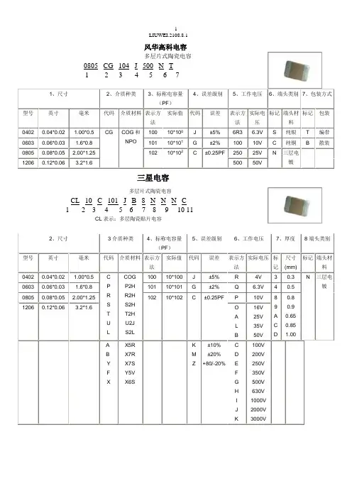
风华高科电容多层片式陶瓷电容0805 CG 104 J 500 N T1 2 3 4 5 6 71、尺寸2、介质种类3、标称电容量(PF)4、误差级别5、工作电压6、端头类别7、包装方式型号英寸毫米代码介质材料表示方法实际值代码误差表示方法实际电压标记端头材料标记包装0402 0.04*0.02 1.00*0.5 CG COG和NPO 100 10*100J ±5% 6R3 6.3V S 纯银T 编带0603 0.06*0.03 1.6*0.8 101 10*101G ±2% 100 10V C 纯铜 B 散装0805 0.08*0.05 2.00*1.25 102 10*102 C ±0.25PF 250 25V N 三层电镀1206 0.12*0.06 3.2*1.6 500 50V三星电容多层片式陶瓷电容CL 10 C 101 J B 8 N N N C1 2 3 4 5 6 7 8 9 10 11CL表示:多层陶瓷贴片电容2、尺寸3介质种类4、标称电容量(PF)5、误差级别6、工作电压7、厚度8端头类别型号英寸毫米代码介质材料表示方法实际值代码误差表示方法实际电压标记尺寸(mm)标记端头材料0402 0.04*0.02 1.00*0.5 CPRSTUL COGP2HR2HS2HT2HU2JS2L100 10*100 J ±5% R 4V 3 0.3 N 三层电镀0603 0.06*0.03 1.6*0.8 101 10*101 G ±2% Q 6.3V 4 0.50805 0.08*0.05 2.00*1.25 102 10*102 C ±0.25PF P 10V 89ACD0.8 0.9 0.650.851.001206 0.12*0.06 3.2*1.6 OALB 16V 25V 35V 50VAB Y F X X5RX7RX7SY5VX6SKMZ±10%±20%+80/-20%CDEFGHIJK100V200V250V350V500V630V1000V2000V3000V国巨(YAGEO)电容多层片式陶瓷电容CC ×××× × ×NPO ×BN ×××1 2 3 4 51、尺寸2、误差精度3、包装形式4、实际电压值5、标称电容量型号英制型号公制代码误差表示方法实际值代码电压代码实际值0201 0603 BCDFGJ±0.1PF±0.25PF±0.5PF±1%±2%±5%R 纸卷盘7inch 7 16V 100 10*1000402 1005 K 吸塑卷盘7inch 8 25V 101 10*101 0603 1608 P 纸卷盘13inch 9 50V 102 10*102 0805 2012 F 吸塑卷盘13inch1206 3216 C 散装1210 32251812 4532TDK贴片电容型号TDK贴片电容的参数识别C 2012 X7R 1H 104 K T系列名称体积材料电压容量误差包装0603=0201 CH 0J=6.3V C=0.25 T=卷带1005=0402 COG 1A=10V D=0.5 B=袋装1608=0603 JB 1C=16V J=5%2012=0805 JF 1E=25V K=10%3216=1206 X7R 1H=50V M=20%3225=1210 X5R 2A=100V Z=+80-20%4532=1812 Y5V 2E=250V5650=2220 2J=630V4520=1808 3A=1KV3D=2KV3F=3KV。
Approval SheetforThick Film Chip ResistorRL series1% 2% 5%YAGEO CORPORATIONFactory: No.11, Min Chuan Rd., Ta Sheh, Kaohsiung, Taiwan, R.O.C.Tel: 886-7-351-4117 Fax: 886-7-352-6475Headquarters: 3F, No.233-1, Pao Chiao Rd., Hsin Tien, Taipei, Taiwan,R.O.C.Tel: 886-2-2917-7555 Fax: 886-2-2917-4286RL Series Version 2000-3 Page-1RL SeriesVersion 2000-3 Page-21. SUBJECT : This specification describes of RL series chip resistors made of YAGEOCorporation by thick film process.2. PART NUMBER : Part number of the chip resistor is identified by the series, size,tolerance, packing style, temperature coefficient, special type and resistance value.Example :RL 1206 F R - 07 0R02Series Size Resistance Packing Temperature Special ResistanceName Code Tolerance Style Coefficient Type Valueof Resistance(1) Size : (unit: inches)0603=0.063×0.033 1210=0.122×0.102 0805=0.083×0.051 2010=0.197×0.098 1206=0.122×0.0632512=0.250×0.126(2) Tolerance : F=±1%, G=±2%, J=±5%(3) Packaging Style : R =Paper Taping Reel. K =Embossed Plastic Tape Reel. C =Bulk Cassette.(4) T .C .R.: “-“Base on Spec.(5) Special Type : 07= 7 inch Dia. Reel10=10 inch Dia. Reel 13=13 inch Dia. Reel(6) Resistance Value : 10m Ω、20 m Ω、51 m Ω、100 m Ω、330 m Ω、470 m Ω……(7) Resistance Series : E24 (E48/96 on request)RL SeriesVersion 2000-3 Page-33. MARKING :(1) RL0805/RL1206/RL1210/RL2010/RL2512Either tolerance in 5% or 1%: 4 digits, uses MIL Standard resistance marking. “R” signifies decimal place.Value =20m Ω(2) RL0603Tolerance in 5%: 3 digits, uses MIL Standard resistance marking. “R” signifies decimal place.Value =220m Ω1% Tolerance : no marking4. POWER RATING(1) Rated Power at 70°C :RL0603=1/10WRL1210=1/3W RL0805=1/8W RL2012=3/4W RL1206=1/4WRL2512=1W(2) Rated Voltage : The DC or AC (rms) continuous working voltage correspondingto the rated power is determined by the following formula : V= √(P X R)Where V= Continuous rated DC or AC (rms) working voltage (V)P= Rated power (W) R= Resistance value (Ω)5. ELECTRICAL CHARACTERISTICSSTYLE RL0603 RL0805 RL1206 Operating Temp. Range -55°C ~ +125°CDerated to 0 Load at +125°CResistance Range 100mΩ≦Rn<1Ω 20mΩ≦Rn<1Ω 10mΩ≦Rn<1ΩTemperature Coefficient ±600ppm/°C±1500ppm/°CSTYLE RL1210 RL2010 RL2512 Operating Temp. Range -55°C ~ +125°CDerated to 0 Load at +125°CResistance Range 10mΩ≦Rn<1Ω 10mΩ≦Rn<1Ω 10mΩ≦Rn<1ΩTemperature Coefficient ±1500ppm/°CRL Series Version 2000-3 Page-4RL SeriesVersion 2000-3 Page-58. ENVIRONMENTAL CHARACTERISTICS(1) Temperature Coefficient of Resistance (T.C.R.)Test Method : Measure resistance at +25°C or specified room temperature asR 1, then measure at -55°C or +125°C respectively as R 2. Determine the temperature coefficient of resistance from the following formula.R 2-R 1 `T.C.R.= ----------------- X 106(PPM/°C) R 1 (t 2-t 1)Where t 1 =+25°C or specified room temperaturet 2 = -55°C or +125°C test temperatureR 1=resistance at reference temperature in ohms. R 2=resistance at test temperature in ohms.Acceptance Standard : (Refer to item 5)(2) Thermal ShockTest Method : -55±3°C, 2 minutes and +125±2°C, 2 minutes as one cycle. After5 cycles, the specimen shall be stabilized at room temperature for 1 hour minimum and then measure the resistance to determine △R/R(%).Acceptance Standard : ±1.0%(3) Low Temperature OperationTest Method : Place the specimen in a test chamber maintained at -65 °C. After one hour stabilization at this temperature, full rated workingvoltage shall be applied 45 minutes. Have15 minutes after remove the voltage, the specimen shall be removed from the chamber and stabilized at room temperature for 24 hrs. Measure the resistance to determine △R/R(%).Acceptance Standard : ±1.0%No mechanical damage.+5+5 -0 +0+0-5+5+5-0RL SeriesVersion 2000-3 Page-6(4) Short Time OverloadTest Method : Apply 2.5 times of rated voltage but not exceeding the maximumoverload voltage for 5 seconds. Have the specimen stabilized at room temperature for 30 minutes minimum. Measure the resistance to determine △R/R(%).Acceptance Standard : ± 1.0% for 1% tolerance± 2.0% for 2~5% toleranceNo evidence of mechanical damage(5) Insulation ResistanceTest Method : Place the specimen in the jig and apply a rated continuesoverload voltage (R.C.O.V) for one minute as shown. Measure the insulation resistance.Type Voltage Type Voltage RL0603 100V RL1210 400V RL0805 300V RL2010 400V RL1206 400V RL2512 400VAcceptance Standard : ≧10000M Ω(6) Dielectric Withstand VoltageTest Method : Place the specimen in the jig and apply a specified valuecontinuous overload voltage as shown for one minute.Type Voltage TypeVoltage RL0603 100V RL1210 400V RL0805 300V RL2010 400V RL1206 400V RL2512 400VAcceptance Standard : Breakdown voltage>specification and without open/short(7) Resistance to Soldering HeatTest Method: Immerse the specimen in the solder pot at 260±5°C for 10±1seconds. Have the specimen stabilized at room temperature for30 minutes minimum.Measure the resistance to determine △R/R(%).Acceptance Standard:±1.0% & no visible damage(8) Moisture ResistanceTest Method: Place the specimen in the test chamber, and subjected to 42damp heat cycles. Each one of which consists of the steps 1 to 7as figure 1. The total length of test is 1000 hours. After the test,have the specimen stabilized at room temperature for 24 hoursand measure the resistance to determine △R/R(%).Acceptance Standard:±2.0% & no visible damageFig.1 Conditions of change of temperatureRL Series Version 2000-3 Page-7RL SeriesVersion 2000-3 Page-8(9) LifeTest Method : Place the specimen in the oven at 70±2°C. Apply the rated voltageto the specimen at the 1.5 hours on and 0.5 hour off cycle. The total length of test is 1000 hours. After the test, have the specimen stabilized at room temperature for one hour minimum and measure the △R/R(%).Acceptance Standard : ± 2.0% for 1% tolerance± 3.0% for 2~5% tolerance(10) SolderabilityTest Method : Immerse the specimen in the solder pot at 230±5°C for 5 sec.Acceptance Standard : At least 95% solder coverage on the termination.9. TAPING REELUnit :mmStyle Packaging Tape width ∅A ∅B ∅C W TRL0603 RL0805 RL1206 RL1210Paper 8mm 180+0-360+1-0 13.0±0.29.0±0.3 11.4±1RL2010 RL2512Embossed 12mm 180+0-360+1-0 13.0±0.213.0±0.3 15.4±1RL SeriesVersion 2000-3 Page-910. PAPER TAPINGUnit : mmDimensionA B W E F P0 P1 P2 ΦD0 TRL0603 1.10±0.1 1.90±0.1 0.70±0.10RL0805 1.65±0.1 2.40±0.1 0.85±0.10RL1206 1.90±0.1 3.50±0.1 0.85±0.10RL12102.80±0.13.50±0.18.0±0.2 1.75±0.13.5±0.054.0±0.14.0±0.052.0±0.051.5+0.1 -00.85±0.1011. EMBOSSED TAPINGDimensionA B W E F P0P1P2ΦD0ΦD1TRL2010 2.8±0.2 5.4±0.2RL2512 3.5±0.2 6.7±0.212.0±0.3 1.75±0.15.5±0.054.0±0.14.0±0.12.0±0.05 1.5±0.1 1.5±0.25 1.0±0.112. PACKING METHODSPAPERRL Series Version 2000-3 Page-10。

贴片铝电解电容规格书丝印说明引言:贴片铝电解电容是一种常见的电子元件,广泛应用于电子设备中。
规格书丝印说明是指印在电容器表面的一些标识和文字,用于表示电容器的参数和特性。
本文将详细介绍贴片铝电解电容规格书丝印说明的含义和解读方法。
一、电容值在贴片铝电解电容规格书丝印说明中,电容值通常以uF为单位表示,例如"100uF"表示电容器的电容值为100微法。
该数值表示了电容器可以储存的电荷量,越大的电容值意味着电容器可以储存更多的电荷。
根据实际需求,可以选择合适的电容值来满足电路的要求。
二、电压值电容器的电压值也是规格书丝印说明中的重要参数之一,通常以V 或者VDC为单位表示,例如"16V"表示电容器的额定工作电压为16伏特。
电压值是指电容器可以承受的最大工作电压,超过该电压可能导致电容器损坏。
在选择电容器时,应根据电路的电压要求选择合适的电压值,以确保电容器的安全工作。
三、温度系数贴片铝电解电容规格书丝印说明中还包含了温度系数的标识,通常以字母表示,例如"E"表示温度系数为-55℃~+105℃。
温度系数是指电容值随温度变化的程度,不同的温度系数对应不同的应用环境。
在高温环境下,应选择具有较高温度系数的电容器,以保证电容值的稳定性。
四、极性贴片铝电解电容是一种极性元件,规格书丝印说明中通常会标明正负极性,例如"+"和"-"符号。
正极性表示电容器的正极,负极性表示电容器的负极,接线时应确保正确连接,否则可能导致电容器损坏。
五、尺寸和外观贴片铝电解电容的规格书丝印说明中还包含了尺寸和外观的标识,通常以数字和字母组合表示,例如"6.3×5.4"表示电容器的尺寸为6.3毫米×5.4毫米。
尺寸和外观标识有助于确定电容器的安装位置和布局,以便于电路设计和组装。
结论:贴片铝电解电容规格书丝印说明提供了关于电容器参数和特性的重要信息,正确解读规格书丝印说明对于选择和使用电容器至关重要。
贴片电容型对照表三星国巨风华选型替代必备 SANY标准化小组 #QS8QHH-HHGX8Q8-GNHHJ8-HHMHGN#风华高科电容多层片式陶瓷电容0805CG104J500NT 1 23 4 5 6 71、尺寸2、介质种类3、标称电容量(PF )4、误差级别5、工作电压6、端头类别7、包装方式型号 英寸 毫米 代码 介质材料 表示方法实际值 代码 误差表示方法 实际电压 标记 端头材料标记 包装 0402 * * CG COG 和NPO 100 10*100J ±5%6R3 S 纯银 T 编带0603 * * 101 10*101G ±2%100 10V C 纯铜 B 散装0805 * * 102 10*102C ±250 25V N 三层电镀 1206**500 50V三星电容多层片式陶瓷电容CL10C101JB8NNNC 1 234 5 6 7 8 9 10 11CL 表示:多层陶瓷贴片电容2、尺寸3介质种类4、标称电容量(PF )5、误差级别6、工作电压7、厚度8端头类别型号 英寸 毫米 代码 介质材料 表示方法实际值 代码 误差表示方法 实际电压 标记 尺寸(mm) 标记 端头材料 0402 * * C P R S T U L COG P2H R2H S2H T2H U2J S2L 100 10*100 J ±5% R 4V 3N 三层电镀 0603 * * 101 10*101 G ±2% Q 40805 * * 102 10*102 C ± P 10V 89 A C D1206**O A L B 16V25V35V50VA ?B ? Y F XX5R X7R X7S Y5V X6SK M Z±10% ±20% +80/-20% C D E F G H I J K 100V200V 250V350V 500V 630V 1000V 2000V 3000V多层片式陶瓷电容CC ×××××× NPO × BN ×××123 45TDK型号TDK贴片电容的参数识别C 2012 X7R 1H 104 K T系列名称体积材料电压容量误差包装0603=0201 CH 0J= C= T=卷带1005=0402 COG 1A=10V D= B=袋装1608=0603 JB 1C=16V J=5%2012=0805 JF 1E=25V K=10%3216=1206 X7R 1H=50V M=20%3225=1210 X5R 2A=100V Z=+80-20% 4532=1812 Y5V 2E=250V5650=2220 2J=630V4520=1808 3A=1KV3D=2KV3F=3KV。
常见电容的识别TDK(东电化)电容识别:C1005COG1E100D T00N(1)(2)(3)(4)(5)(6)(7)(8)(1)产品类型:多层片式陶瓷电容。
(2)封装尺寸:型号公制型号英制长×宽050302010.5×0.25mm10050402 1.0×0.5mm16080603 1.5×0.76mm20120805 2.0×1.25mm32161206 3.2×1.6mm32251210 3.2×2.5mm45321812 4.5×3.2mm(3)温度特性(介质材料):一般有COG、X5R、X7V、Y5V、Z5U。
(4)额定电压:代码额定电压0J 6.3V1A10V1C16V1E25V1H50V2A100V2E250V2J630V3A1000V3D2000V3F3000V(5)标称电容量:代码电容量0R50.5pF3R5 3.5pF010 1.0pF10010pF102 1.0nF10310nF105 1.0uF10610uF(6)电容容差(误差精度):代码误差精度适用范围A ±0.05pF 等于或小于10pFB ±0.10pFC ±0.25pFD ±0.50pF F ±1.0pF F ±1.0%10pF 以上G ±2.0%J ±5.0%K ±10%L ±15%M ±20%Z+80/-20%(7)包装类型:代码包装类型B 袋装T编带(8)TDK 自用编码:MURATA (村田)电容识别:GR M 188B11H 102K A01D(1)(2)(3)(4)(5)(6)(7)(8)(9)(10)(1)产品编号:(2)系列号:(3)封装尺寸:代码型号英制长×宽02010050.4×0.2mm 0302010.6×0.3mm 0502020.5×0.5mm 0803030.8×0.8mm 0D 0150150.38×0.38mm 0M 03020.9×0.6mm 110504 1.25×1.0mm 150402 1.0×0.5mm 180603 1.6×0.8mm 1M 0504 1.37×1.0mm 210805 2.0×1.25mm 221111 2.8×2.8mm 311206 3.2×1.6mm 3212103.2×2.5mm421808 4.5×2.0mm431812 4.5×3.2mm522211 5.7×2.0mm552220 5.7×5.0mm (4)电容厚度:代码电容厚度20.2mm2两单元(阵列芯片类)30.3mm4四单元(阵列芯片类)50.50mm60.60mm70.70mm80.80mm90.85mmA 1.00mmB 1.25mmC 1.60mmD 2.00mmE 2.50mmF 3.20mmM 1.15mmN 1.35mmQ 1.50mmR 1.80mmS 2.80mmX根据个人标准(5)温度特性(介质材料):代码介质材料5C COGD7X7TF5Y5VR6X5RR7X7R(6)额定电压:代码额定电压0E 2.5V0G 4.0V0J 6.3V1A10V1C16V1E25VYA35V1H 50V 2A 100V 2D 200V 2E 250V YD 300V 2H 500V 2J 630V 3A 1000V 3D 2000V 3F3150V (7)标称电容量:代码电容量R500.5pF 1R0 1.0pF 010 1.0pF 10010pF 102 1.0nF 1051.0uF(8)电容容差(误差精度):代码误差精度适用范围W ±0.05pF 等于或小于10pFB ±0.1pFC ±0.25pFD ±0.5pF G ±2%大于10pFJ ±5%K ±10%M ±20%Z +80/-20%R根据个人标准(9)MURATA 自用编码:(10)包装编码:TAIYO YUDEN (太阳诱电)电容识别:J M K316BJ 106M L-T(1)(2)(3)(4)(5)(6)(7)(8)(9)(10)(1)额定电压:代码额定电压P 2.5V A 4.0V J6.3VL 10V E 16V T 25V G 35V U50V(2)系列号:(3)端电极类型:代码端电极类型K电镀(4)封装尺寸:代码型号英制长×宽1050402 1.0×0.5mm 1070603 1.6×0.8mm 2120805 2.0×1.25mm 3161206 3.2×1.6mm 32512103.2×2.5mm (5)温度特性(介质材料):代码介质材料F Y5V BJ X7R 或X5RCGCOG (6)标称电容量:代码电容量0R50.5pF 3R5 3.5pF 010 1.0pF 10010pF 102 1.0nF 10310nF 105 1.0uF 10610uF(7)电容容差(误差精度):代码误差精度适用范围A ±0.05pF 等于或小于10pFB ±0.10pFC ±0.25pFD ±0.50pF F ±1.0pF F ±1.0%10pF 以上G ±2.0%J ±5.0%K ±10%L±15%M±20%Z+80/-20%(8)电容厚度:代码电容厚度K0.45mmA0.80mmD0.85mmF 1.15mmG 1.25mmH 1.50mmL 1.60mmN 1.90mmY 2.00mmM 2.50mm(9)特殊编号:代码包装类型-标准产品(10)包装类型:代码包装类型B袋装T编带KYOCERAAVX(京瓷)电容识别:CM21X7R105K10A T000(1)(2)(3)(4)(5)(6)(7)(8)(9)(1)产品编码:代码用途CM普通应用CT薄型尺寸DM/DR汽车应用CF耐高压CA多联型CU高频用低ESR(2)封装尺寸:代码型号公制型号英制长×宽03060302010.6×0.3mm0510050402 1.0×0.5mm10516080603 1.6×0.8mm2120120805 2.0×1.25mm31632161206 3.2×1.6mm3232251210 3.2×2.5mm4245201808 4.5×2.0mm 4345321812 4.5×3.2mm 5257202208 5.7×2.0mm 55575022205.7×5.0mm(3)温度特性(介质材料):一般有X5R 、X7V 、Y5V 。
贴片电容的材质规格贴片电容的材质规格贴片电容(MLCC)Multilayer Ceramic Capacitor常规贴片电容按材料分为COG(NPO)、X7R、Y5V,常见封装有0201、0402、0603、0805、1206、1210、1812、2010。
NPO、X7R、Z5U和Y5V的主要区别是它们的填充介质不同。
在相同的体积下由于填充介质不同所组成的电容器的容量就不同,随之带来的电容器的介质损耗、容量稳定性等也就不同。
所以在使用电容器时应根据电容器在电路中作用不同来选用不同的电容器。
上表可看出各个不同材料的温度特性一 NPO电容器NPO是一种最常用的具有温度补偿特性的单片陶瓷电容器。
它的填充介质是由铷、钐和一些其它稀有氧化物组成的。
NPO电容器是电容量和介质损耗最稳定的电容器之一。
在温度从-55℃到+125℃时容量变化为0±30ppm/℃,电容量随频率的变化小于±0.3ΔC。
NPO电容的漂移或滞后小于±0.05%,相对大于±2%的薄膜电容来说是可以忽略不计的。
其典型的容量相对使用寿命的变化小于±0.1%。
NPO电容器随封装形式不同其电容量和介质损耗随频率变化的特性也不同,大封装尺寸的要比小封装尺寸的频率特性好。
NPO电容器适合用于振荡器、谐振器的槽路电容,以及高频电路中的耦合电容。
二 X7R电容器X7R电容器被称为温度稳定型的陶瓷电容器。
当温度在-55℃到+125℃时其容量变化为15%,需要注意的是此时电容器容量变化是非线性的。
X7R电容器的容量在不同的电压和频率条件下是不同的,它也随时间的变化而变化,大约每10年变化1%ΔC,表现为10年变化了约5%。
X7R电容器主要应用于要求不高的工业应用,而且当电压变化时其容量变化是可以接受的条件下。
它的主要特点是在相同的体积下电容量可以做的比较大。
三 Z5U电容器Z5U电容器称为”通用”陶瓷单片电容器。