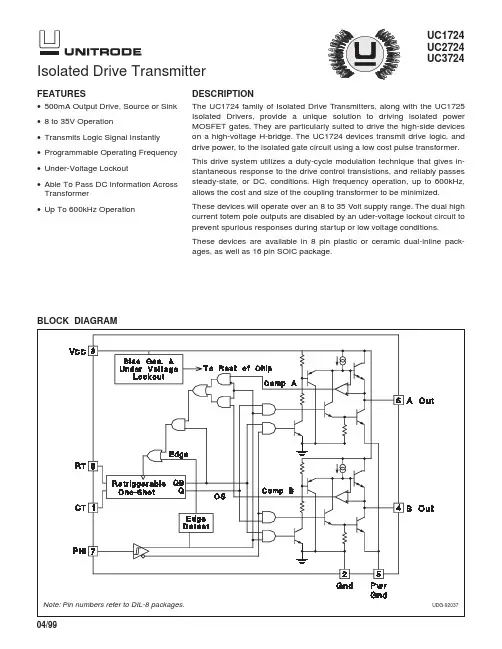
UC2724 UC3724FEATURES•500mA Output Drive, Source or Sink •8 to 35V Operation•Transmits Logic Signal Instantly •Programmable Operating Frequency •Under-Voltage Lockout•Able To Pass DC Information Across Transformer•Up To 600kHz Operation DESCRIPTIONThe UC1724family of Isolated Drive Transmitters,along with the UC1725 Isolated Drivers,provide a unique solution to driving isolated power MOSFET gates.They are particularly suited to drive the high-side devices on a high-voltage H-bridge.The UC1724devices transmit drive logic,and drive power, to the isolated gate circuit using a low cost pulse transformer.This drive system utilizes a duty-cycle modulation technique that gives in-stantaneous response to the drive control transistions,and reliably passes steady-state,or DC,conditions.High frequency operation,up to600kHz, allows the cost and size of the coupling transformer to be minimized.These devices will operate over an8to35Volt supply range.The dual high current totem pole outputs are disabled by an uder-voltage lockout circuit to prevent spurious responses during startup or low voltage conditions.These devices are available in8pin plastic or ceramic dual-inline pack-ages, as well as 16 pin SOIC package.Isolated Drive TransmitterBLOCK DIAGRAMUDG-92037 Note:Pin numbers refer to DIL-8 packages.CONNECTION DIAGRAMSELECTRICAL CHARACTERISTICS:Unless otherwise stated, V CC = 20V, R T = 4.3k Ω, C T = 1000pF, no load on anyoutput and these specifications apply for: –55o C < T A < 125o C for the UC1724, –25o C < T A < 85o C for the UC2724, and 0o C < T A < 70o C for the UC3724. T A =T J .PARAMETERTEST CONDITIONSMINTYPMAX UNITS Under-Voltage Lockout Start-Up Threshold V IN Rising7.759.5V Threshold Hysteresis 0.41.01.5V Retriggerable One-Shot Initial Accuracy T J = 25°C 1.54 1.92.25µs Temperature Stability Over Operating T J 1.02.9µs Voltage Stability V IN = 10 to 35V 0.20.5%/V Operating Frequency L LOAD = 1.4mH 100150200kHz Minimum Pulse Width RT = 2k CT = 300pF1005001200ns Operating FrequencyRT = 2k C T = 300pF L LOAD = 1.4mH5007501100kHzABSOLUTE MAXIMUM RATINGSSupply Voltage V IN . . . . . . . . . . . . . . . . . . . . . . . . . . . . . . .40V Source/Sink Current (Pulsed). . . . . . . . . . . . . . . . . . . . . . . .1A Source/Sink Current (Continuous). . . . . . . . . . . . . . . . . . .0.5A Ouput Voltage (Pins 4, 6). . . . . . . . . . . . . . .–0.3 to (V IN +0.3)V P HI , R T , and C T inputs (Pins 1, 7, and 8). . . . . . . . .–0.3 to 6V Operating Junction Temperature (Note 2). . . . . . . . . . . .150°C Storage Temperature Range . . . . . . . . . . . . . .–65°C to 150°C Lead Temperature (Soldering, 10 Seconds). . . . . . . . . .300°C Note 1:All voltages are with respect to GND (Pin 2);all cur-rents are positive into, negative out of part.Note 2:Consult Unitrode Integrated Circuit Databook for ther-mal limitations and considerations of package.Note 3:Pin numbers refer to DIL-8 packages.RECOMMENDED OPERATION CONDITIONSInput Voltage . . . . . . . . . . . . . . . . . . . . . . . . . . . . .+9V to +35V Sink/Source Load Current (each output). . . . . . . . .0 to 500mA Timing Resistor. . . . . . . . . . . . . . . . . . . . . . . . . . .2kW to 10kW Timing Capacitor . . . . . . . . . . . . . . . . . . . . . . . . .300pF to 3nF Operating Temperature Range (UC1724). . .–55°C<T A <125°C Operating Temperature Range (UC3724). . . . . .0°C<T A <70°C Note 4:Range over which the device is functional andparameter limits are guaranteed.TEMPERATURE RANGE PACKAGE UC1724J –55°C to +125°C CDIPUC2724DW –25°C to +85°C SOIC-Wide UC2724N PDIPUC3724DW 0°C to +70°CSOIC-Wide UC3724NPDIPORDERING INFORMATIONELECTRICAL CHARACTERISTICS:Unless otherwise stated, V CC = 20V, R T = 4.3k Ω, C T = 1000pF, no load on anyoutput and these specifications apply for: –55o C < T A < 125o C for the UC1724, –25o C < T A < 85o C for the UC2724, and 0o C < T A < 70o C for the UC3724. T A =T J .PARAMETERTEST CONDITIONSMINTYPMAX UNITSPhi Input (Control Input)HIGH Input Voltage 2.0V LOW Input Voltage 0.8V HIGH Input Current V IH =+2.4V –220–130µA LOW Input Current V IL =+0.4V–600–300µA Delay to One-Shot 350ns Delay to Output 250nsOutput Drivers Output Low LevelI SINK = 50mA 0.30.4V I SINK = 250mA 0.5 2.1V Output High Level (Volts Below V CC )I SOURCE = 50 mA 1.5 2.1V I SOURCE = 250 mA 1.7 2.5V Rise/Fall Time No load3090nsTotal Supply Current Supply CurrentC T = 1.4V1530mAUNITRODE CORPORA TION7 CONTINENTAL BLVD.• MERRIMACK, NH 03054TEL.(603) 424-2410FAX (603) 424-3460Additional InformationPlease refer to the following Unitrode application topics.[1]Application Note U-127,Unique Chip Pair Simplified Isolated High-Side Switch Drive by John A.O’Connor.[2]Design Note DN-35,IGBT Drive Using MOSFET Gate Drivers by John A.O’Conner.IMPORTANT NOTICETexas Instruments and its subsidiaries (TI) reserve the right to make changes to their products or to discontinue any product or service without notice, and advise customers to obtain the latest version of relevant information to verify, before placing orders, that information being relied on is current and complete. All products are sold subject to the terms and conditions of sale supplied at the time of order acknowledgement, including those pertaining to warranty, patent infringement, and limitation of liability.TI warrants performance of its semiconductor products to the specifications applicable at the time of sale in accordance with TI’s standard warranty. Testing and other quality control techniques are utilized to the extent TI deems necessary to support this warranty. Specific testing of all parameters of each device is not necessarily performed, except those mandated by government requirements.CERTAIN APPLICATIONS USING SEMICONDUCTOR PRODUCTS MAY INVOLVE POTENTIAL RISKS OF DEATH, PERSONAL INJURY, OR SEVERE PROPERTY OR ENVIRONMENTAL DAMAGE (“CRITICAL APPLICATIONS”). TI SEMICONDUCTOR PRODUCTS ARE NOT DESIGNED, AUTHORIZED, OR WARRANTED TO BE SUITABLE FOR USE IN LIFE-SUPPORT DEVICES OR SYSTEMS OR OTHER CRITICAL APPLICATIONS. INCLUSION OF TI PRODUCTS IN SUCH APPLICATIONS IS UNDERSTOOD TO BE FULLY AT THE CUSTOMER’S RISK.In order to minimize risks associated with the customer’s applications, adequate design and operating safeguards must be provided by the customer to minimize inherent or procedural hazards.TI assumes no liability for applications assistance or customer product design. TI does not warrant or represent that any license, either express or implied, is granted under any patent right, copyright, mask work right, or other intellectual property right of TI covering or relating to any combination, machine, or process in which such semiconductor products or services might be or are used. TI’s publication of information regarding any third party’s products or services does not constitute TI’s approval, warranty or endorsement thereof.Copyright © 1999, Texas Instruments Incorporated。