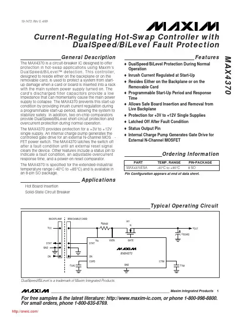
For free samples & the latest literature: , or phone 1-800-998-8800.For small orders, phone 1-800-835-8769.General DescriptionThe MAX4370 is a circuit-breaker IC designed to offer protection in hot-swap applications using Maxim’s DualSpeed/BiLevel™ detection. This controller,designed to reside either on the backplane or on the removable card, is used to protect a system from start-up damage when a card or board is inserted into a rack with the main system power supply turned on. The card’s discharged filter capacitors provide a low impedance that can momentarily cause the main power supply to collapse. The MAX4370 prevents this start-up condition by providing inrush current regulation during a programmable start-up period, allowing the system to stabilize safely. In addition, two on-chip comparators provide DualSpeed/BiLevel short-circuit protection and overcurrent protection during normal operation.The MAX4370 provides protection for a +3V to +12V single supply. An internal charge pump generates the controlled gate drive for an external N-channel MOS -FET power switch. The MAX4370 latches the switch off after a fault condition until an external reset signal clears the device. Other features include a status pin to indicate a fault condition, an adjustable overcurrent response time, and a power-on reset comparator.The MAX4370 is specified for the extended-industrial temperature range (-40°C to +85°C) and is available in an 8-pin SO package.ApplicationsHot Board InsertionSolid-State Circuit BreakerFeatureso DualSpeed/BiLevel Protection During Normal Operation o Inrush Current Regulated at Start-Up o Resides Either on the Backplane or on the Removable Card o Programmable Start-Up Period and Response Time o Allows Safe Board Insertion and Removal from Live Backplane o Protection for +3V to +12V Single Supplies o Latched Off After Fault Condition o Status Output Pino Internal Charge Pump Generates Gate Drive for External N-Channel MOSFETMAX4370Current-Regulating Hot-Swap Controller withDualSpeed/BiLevel Fault Protection________________________________________________________________Maxim Integrated Products1Typical Operating Circuit19-1472; Rev 0; 4/99Ordering InformationPin Configuration appears at end of data sheet.M A X 4370Current-Regulating Hot-Swap Controller with DualSpeed/BiLevel Fault Protection 2_______________________________________________________________________________________ABSOLUTE MAXIMUM RATINGSELECTRICAL CHARACTERISTICS(V IN = +2.7V to +13.2V, T A = -40°C to +85°C, unless otherwise noted. Typical values are at V IN = +5V and T A = +25°C.) (Note 2)Stresses beyond those listed under “Absolute Maximum Ratings” may cause permanent damage to the device. These are stress rating s only, and functional operation of the device at these or any other conditions beyond those indicated in the operational sections of the specificatio ns is not implied. Exposure to absolute maximum rating conditions for extended periods may affect device reliability.Note 1:ON can be pulled below ground. Limiting the current to 2mA ensures that this pin is never lower than about -0.8V.V IN to GND...........................................................................+15V STAT to GND..........................................................-0.3V to +14V GATE to GND ..............................................-0.3V to (V IN + 8.5V)ON to GND (Note 1).................................................-1V to +14V CSPD to GND.............-0.3V to the lower of (V IN + 0.3V) or +12V VSEN, CTIM to GND....................................-0.3V to (V IN + 0.3V) Current into ON...................................................................±2mACurrent into Any Other Pin................................................±50mA Continuous Power Dissipation (T A = +70°C)SO (derate 5.9mW/°C above +70°C)...........................471mW Operating Temperature Range ...........................-40°C to +85°C Storage Temperature Range.............................-65°C to +150°C Lead Temperature (soldering, 10sec)............................+300°CMAX4370Current-Regulating Hot-Swap Controller withDualSpeed/BiLevel Fault Protection_______________________________________________________________________________________3ELECTRICAL CHARACTERISTICS (continued)(V IN = +2.7V to +13.2V, T A = -40°C to +85°C, unless otherwise noted. Typical values are at V IN = +5V and T A = +25°C.) (Note 2)Note 2:All devices are 100% tested at T A = +25°C. All temperature limits are guaranteed by design.Note 3:The start-up period (t START ) is the time during which the slow comparator is ignored and the device acts as a current limiterby regulating the sense current with the fast comparator. It is measured from ON rising above 0.6V to STAT rising.Note 4:The current available at GATE is a function of V GATE (see Typical Operating Characteristics.)M A X 4370Current-Regulating Hot-Swap Controller with DualSpeed/BiLevel Fault Protection 4_______________________________________________________________________________________Typical Operating Characteristics(Circuit of Figure 7, V IN = 5V, R SENSE = 100m Ω, M1 = FDS6670A, C BOARD = 470µF, C GATE = 0, R S = 0, T A = +25°C, unless other-wise noted.)00.30.20.10.50.40.90.80.70.61.02468101214SUPPLY CURRENT vs. INPUT VOLTAGEV IN (V)S U P P L Y C U R R E N T (m A )-40-1510356085SUPPLY CURRENT vs. TEMPERATURETEMPERATURE (°C)00.30.20.10.50.40.90.80.70.61.0S U P P L Y C U R R E N T (m A )49.049.649.449.250.049.850.850.650.450.251.002468101214SLOW COMPARATOR THRESHOLDvs. INPUT VOLTAGEV IN (V)V S C , T H (m V )2001004003006005007001101001000FAST COMPARATOR RESPONSE TIMEvs. OVERDRIVE VOLTAGEV OD (mV)t F C D (n s )182019222123241820192221232406824101214SLOW COMPARATORRESPONSE TIME vs. INPUT VOLTAGEV IN (V)t C S P D (µs )t C S P D (m s)190196194192200198108206204202210FAST COMPARATOR THRESHOLDvs. INPUT VOLTAGEV F C , T H (m V )02468101214V IN (V)400430420410450440490480470460500-40-2020406080100FAST COMPARATOR RESPONSE TIMEvs. TEMPERATURETEMPERATURE (°C)t F C D (n s )2502703102903303504268101214START-UP TIME vs. INPUT VOLTAGEV IN (V)t S T A R T (µs )252731293335t S T A R T (m s )MAX4370Current-Regulating Hot-Swap Controller withDualSpeed/BiLevel Fault Protection_______________________________________________________________________________________506040208010012008624101214161820GATE CHARGE CURRENT vs. GATE VOLTAGEV GATE (V)I G A T E (µA )502510075125150-40-1035-156085GATE CHARGE CURRENT vs. TEMPERATURETEMPERATURE (°C)I G A T E (µA )5151020254268101214GATE VOLTAGE vs. INPUT VOLTAGEV IN (V)V G A T E (V )01005015030035025020040004681021214161820GATE DISCHARGE CURRENTvs. GATE VOLTAGEV GATE (V)I G A T E (µA)C BOARD = 0, R SENSE = 100m Ω,C TIM = 10nF, C GATE = 0V OUT (2V/div)V GATE (2V/div)ON 100µs/divSTART-UP TIME (C BOARD = 0)MAX4370-1610050200150350300250400GATE DISCHARGE CURRENTvs. TEMPERATURETEMPERATURE (°C)I G A T E (µA)C BOARD = 470µF, R SENSE = 100m Ω,C TIM = 10nF, C GATE= 0I LOAD (1A/div)V OUT (2V/div)V GATE (2V/div)ON 500µs/divSTART-UP TIME (C BOARD = 470µF)MAX4370-15C BOARD = 470µF, R SENSE = 100m Ω,C GATE= 22nF, C TIM = 10nF, R S = 0I LOAD (1A/div)V OUT (2V/div)V GATE (2V/div)ON 1ms/divSTART-UP TIME(EXTERNAL C GATE = 22nF, C BOARD = 470µF)MAX4370-17C BOARD = 470µF, R SENSE = 100m Ω,C GATE = 0I LOAD (1A/div)V OUT (2V/div)V GATE (2V/div)0A50µs/divTURN-OFF TIME (C BOARD = 470µF)MAX4370-18ON0VTypical Operating Characteristics (continued)(Circuit of Figure 7, V IN = 5V, R SENSE = 100m Ω, M1 = FDS6670A, C BOARD = 470µF, C GATE = 0, R S = 0, T A = +25°C, unless other-wise noted.)M A X 4370Current-Regulating Hot-Swap Controller with DualSpeed/BiLevel Fault Protection 6_______________________________________________________________________________________Typical Operating Characteristics (continued)(Circuit of Figure 7, V IN = 5V, R SENSE = 100m Ω, M1 = FDS6670A, C BOARD = 470µF, C GATE = 0, R S = 0, T A = +25°C, unless other-wise noted.)C BOARD = 0, R SENSE = 100m Ω,C GATE = 0, R S = 0I LOAD(1A/div)V OUT(2V/div)V GATE (2V/div)050µs/divTURN-OFF TIME (C BOARD = 0)MAX4370-19ONA0VC BOARD = 470µF, R SENSE = 100m Ω,C GATE = 22nF, R S = 0ILOAD (1A/div)V OUT (2V/div)V GATE (2V/div)0A0V200µs/divTURN-OFF TIME(EXTERNAL C GATE = 22nF, C BOARD = 470µF)MAX4370-20ON 0.010.11101001000TIME TO CHARGE GATEvs. C GATEC GATE (nF)T I M E T O C H A R G E G A T E (m s )10000.0010.0110.1100100.010.11101001000TIME TO DISCHARGE GATEvs. C GATEC GATE (nF)T I M E T O D I S C H A R G E G A T E (m s )10000.00110.10.01101000.5950.5970.6010.5990.6030.60504268101214ON COMPARATOR THRESHOLDvs. INPUT VOLTAGEV IN (V)O N C O M P A R A T O R T H R E S H O L D D (V )0.59500.60000.59750.60500.60250.60750.6100-403560-151085ON COMPARATOR THRESHOLDvs. TEMPERATURETEMPERATURE (°C)O N C O M P A R A T O R T H R E S H O L D (V )R I S I N GF A L L I NG 2.302.402.352.502.452.552.60-403560-151085UVLO THRESHOLD VOLTAGEvs. TEMPERATURETEMPERATURE (°C)U V L O T H R E S H O L D (V )140145150155160UVLO DELAY vs. TEMPERATURETEMPERATURE (°C)U V L O D E L A Y (m s )-403560-151085MAX4370Current-Regulating Hot-Swap Controller withDualSpeed/BiLevel Fault Protection_______________________________________________________________________________________7Pin DescriptionPIN Supply Voltage Input. Connect to 2.7V to 13.2V.V IN 1FUNCTIONNAME Current-Sense Resistor Voltage Input. R SENSE is connected from V IN to VSEN.VSEN 2GroundGND 4Gate Drive Output. Connect to gate of external N-channel MOSFET.GATE 3Start-Up Timer Setting. Leave floating or connect the timing capacitor from CTIM to GND. See Start-Up Timing Capacitor section.CTIM 6ON Comparator Input. Connect high for normal operation; connect low to force the MOSFET off. Comparator threshold V TH,ON = 0.6V allows for precise control over shutdown feature. Pulse ON low for at least 20µs,then high to restart after a fault.ON8Status Output—open drain. High indicates start-up completed with no fault. See Table 1.STAT 7Slow Comparator Speed Setting. Leave floating or connect the timing capacitor from CSPD to GND. See Slow Comparator Response Time section.CSPD 5Figure 1. Functional DiagramM A X 4370Current-Regulating Hot-Swap Controller with DualSpeed/BiLevel Fault Protection 8_______________________________________________________________________________________Detailed DescriptionThe MAX4370 is a circuit-breaker IC designed for hot-swap applications where a card or board is to be inserted into a rack with the main system power supply turned on. Normally, when a card is plugged into a live backplane, the card is discharged filter capacitors pro-vide a low impedance, which can momentarily cause the main power supply to collapse. The MAX4370 is designed to reside either in the backplane or in the removable card to provide inrush-current limiting and short-circuit protection. This is achieved using a charge pump as gate drive for an external N-channel MOSFET,an external current-sense resistor, and two on-chip comparators. Figure 1 shows the device’s functional diagram.The slow comparator response time and the start-up timer can be adjusted with external capacitors. The tim-ing components are optional; without them the part is set to its nominal values, as shown in the Electrical Characteristics.Start-Up PeriodCTIM sets the start-up period. This mode starts when the power is first applied to V IN if ON is connected to V IN , or at the rising edge of ON. In addition, the voltage at V IN must be above the undervoltage lockout for 150ms (see Undervoltage Lockout ).During start-up, the slow comparator is disabled and current limiting is provided two different ways:1)Slow ramping of the current to the load by controlling the external MOSFET gate voltage.2)Limiting the current to the load by regulating the volt-age across the external current-sense resistor.Unlike other circuit-breaker ICs, the MAX4370 hot-swap controller regulates the current to a preset level instead of completely turning off if an overcurrent occurs during start-up.In start-up mode, the gate drive current is limited to 100µA and decreases with the increase of the gate voltage (see Typical Operating Characteristics ). This allows the MAX4370 to slowly enhance the MOSFET. If the fast comparator detects an overcurrent, the gate voltage is momentarily discharged with a fixed 80µA current until the load current through the sense resistor (R SENSE ) decreases below its threshold point. This effectively regulates the turn-on current during start-up.Figure 2 shows the start-up waveforms. STAT goes high at the end of the start-up period if no fault condi-tion is present.Normal Operation (DualSpeed/BiLevel)In normal operation (after the start-up period has expired), protection is provided by turning off the exter-nal MOSFET when a fault condition is encountered.DualSpeed/BiLevel fault protection incorporates two comparators with different thresholds and response times to monitor the load current:1)Slow Comparator. This comparator has an externally set response time (20µs to seconds) and a fixed 50mV threshold voltage. The slow comparator ignores low-amplitude momentary current glitches.After an extended overcurrent condition, a fault is detected and the MOSFET gate is discharged.2)Fast Comparator. This comparator has a fixed response time and a higher 200mV threshold volt -age. The fast comparator turns off the MOSFET immediately after it detects a large amplitude event such as a short circuit.In each case, when a fault is encountered, the status pin (STAT) goes low and the MAX4370 stays latched off. Figure 3 shows the waveforms after a fault condi -tion.Figure 2. Start-Up WaveformsMAX4370Current-Regulating Hot-Swap Controller withDualSpeed/BiLevel Fault Protection_______________________________________________________________________________________9Slow ComparatorThe slow comparator is disabled at start-up while the external MOSFET is turning on. This allows the part to ignore the higher-than-normal inrush current charging the board capacitors (C BOARD ) when a card is first plugged in.If the slow comparator detects an overload current while in normal operation (after start-up is completed),it turns off the external MOSFET by discharging the gate capacitance with a 200µA current. The slow com-parator threshold is set at 50mV and has a default delay of 20µs (CSPD floating), allowing it to ignore power-supply glitches and noise. The response time can be lengthened with an external capacitor at CSPD (Figure 8).If the overcurrent condition is not continuous, the dura-tion above the threshold minus the duration below it must be greater than 20µs (or the external programmed value) for the device to trip. When the current is above the threshold, CSPD is charged with a 6µA current source; when the current is below the threshold, CSPD is discharged with a 6µA current source. A fault is detected when CSPD is charged to the trip point of 1.2V. A pulsing current with a duty cycle greater than50% (i.e., > 50% of the time the current is above the threshold level) will be considered a fault condition even if it is never higher than the threshold for more than the slow comparator’s set response time.Once the fault condition is detected, the STAT pin goes low and the device goes into latched mode. The GATE voltage discharge rate depends on the gate capaci-tance and the external capacitance at GATE.Fast ComparatorThe fast comparator behaves differently according to the operating mode. During start-up, the fast compara-tor is part of a simple current regulator. When the sensed current is above the threshold (V FC,TH =200mV), the gate is discharged with a 80µA current source. When the sensed current drops below the threshold, the charge pump turns on again. The sensed current will rise and fall near the threshold due to the fast comparator and charge-pump propagation delay.The gate voltage will be roughly saw-tooth shaped, and the load current will present a 20% ripple. The ripple can be reduced by adding a capacitor from GATE to GND. Once C BOARD is completely charged, the load current drops to its normal operating levels. If the sensed current is still high after the start-up timer expires, the MOSFET gate is discharged completely.In normal operation (after start-up), the fast comparator is used as an emergency off switch. If the load current reaches the fast comparator threshold, the device immediately forces the MOSFET off completely by dis-charging the GATE with a 200µA current. This can occur in the event of a serious current overload or a dead short. Given a 1000pF gate capacitance and 12V gate voltage, the MOSFET will be off in less than 60µs.Any additional capacitance connected between GATE and GND to slow down the turn-on time also increases the turn-off time.Latched Mode and ResetThe MOSFET driver of the MAX4370 stays latched off after a fault condition until it is reset by a negative-going pulse on the ON pin. Pulse ON low for 20µs (min), then high to restart after a fault. During start-up, a negative-going edge on ON will force the device to turn off the MOSFET and place the device in latched mode.Keep ON low for 20µs (min) to restart.Figure 3. Response to a Fault ConditionM A X 4370Current-Regulating Hot-Swap Controller with DualSpeed/BiLevel Fault Protection 10______________________________________________________________________________________Status OutputThe status output is an open-drain output that goes low when the part is:1)in start-up2)forced off (on = GND)3)in an overcurrent condition, or 4)latched off.STAT is high only if the part is in normal mode and no faults are present (Table 1). Figure 4 shows the STAT timing diagram.Over/Undervoltage LockoutsThe undervoltage lockout prevents the MAX4370 from turning on the external MOSFET until the input voltage at V IN exceeds the lockout threshold (2.25V min) for at least 150ms. The undervoltage lockout protects the external MOSFET from insufficient gate drive voltage.The 150ms timeout ensures that the board is fully plugged into the backplane and that V IN is stable.Voltage transients at V IN with voltages below the UVLO will reset the device and initiate a start-up sequence.The device also features a gate overvoltage lockout that prevents the device from restarting after a fault condition if the discharge has not been completed.V GATE must be discharged to below 0.1V before restarting. Since the MAX4370 does not monitor the output voltage, a start-up sequence can be initiated while the board capacitance is still charged.Gate Overvoltage ProtectionNewer-generation MOSFETs have an absolute maxi -mum rating of ±8V for the gate-to-source voltage (V GS ).To protect these MOSFETs, the MAX4370 limits the gate-to-drain (V GD ) to +7.5V with an internal zener diode. No protection is provided for negative V GD . If GATE can be discharged to GND faster than the output voltage, an external small-signal protection diode (D1)can be used, as shown in Figure 5.Table 1. Status Output Truth TableFigure 4. Status Output (STAT) Timing DiagramFigure 5. External Gate-Source ProtectionX = Don’t care分销商库存信息:MAXIMMAX4370ESA+MAX4370ESA+T。