STM32自学笔记
- 格式:pptx
- 大小:4.55 MB
- 文档页数:60
《STM32Cube高效开发教程》读书笔记目录一、前言 (2)1.1 书籍简介 (3)1.2 编写目的 (4)二、STM32Cube概述 (5)2.1 STM32Cube的意义 (6)2.2 STM32Cube的主要特点 (7)三、安装与配置 (9)3.1 STM32Cube的安装 (10)3.2 开发环境的配置 (11)四、创建项目 (12)4.1 新建项目 (13)4.2 项目设置 (14)五、HAL库介绍 (15)5.1 HAL库简介 (16)5.2 HAL库的主要组件 (18)六、STM32最小系统 (19)6.1 STM32最小系统的组成 (21)6.2 STM32最小系统的应用 (22)七、GPIO操作 (24)7.1 GPIO的基本概念 (25)7.2 GPIO的操作方法 (26)八、中断系统 (28)8.1 中断的基本概念 (29)8.2 中断的处理过程 (31)九、定时器 (33)9.1 定时器的功能介绍 (34)9.2 定时器的操作方法 (36)十五、文件系统 (37)一、前言随着科技的飞速发展,嵌入式系统已广泛应用于我们生活的方方面面,从智能手机到自动驾驶汽车,其重要性不言而喻。
而STM32作为一款广泛应用的微控制器系列,以其高性能、低功耗和丰富的外设资源赢得了广大开发者的青睐。
为了帮助开发者更好地掌握STM32系列微控制器的开发技巧,提升开发效率,我们特别推出了《STM32Cube 高效开发教程》。
本书以STM32Cube为核心,通过生动的实例和详细的讲解,全面介绍了STM32系列微控制器的开发过程。
无论是初学者还是有一定基础的开发者,都能从中找到适合自己的学习内容。
通过本书的学习,读者将能够更加深入地理解STM32的内部结构和工作原理,掌握其编程方法和调试技巧,从而更加高效地进行嵌入式系统的开发和应用。
在科技日新月异的今天,STM32系列微控制器将继续扮演着举足轻重的角色。
stm32学习经历(5篇可选)第一篇:stm32学习经历随便写写,关于stm32 最近在学习stm32,写点东西,虽然简单,但都是原创啊开发板是前辈画的,好像是用来测试一个3G功能的,不过对于我来说太远;我要来了3个,自己焊了一个最小系统,好在公司资源还是不错的,器件芯片有,还可以问问前辈--对公司还是比较满意的,虽然工资少了点,但学东西第一位O(∩_∩)O~。
最开始当然是建工程了,这个真不太会,前前后后竟用了一周(时间真长,别见笑啊),上网查资料,问前辈,自己琢磨。
总算搞定,然后从GPIO开始学,开始还真没什么头绪(虽然在大学学点51,但完全没有真正应用,顶多是跑马灯实验),开始纠结是从寄存器开始学还是从库函数开始学,后来看到一句“用库函数入门,用寄存器提高”于是下定决心用库,但当时没有库的概念,结果走了很多弯路,看了很多不必要的东西,当时竟没理解到只是调用库就OK了,别的不用管。
最后潜心的在教程网看完一个例程后照猫画虎写了一个,经过了多次调试以后,灯终于亮了!那个兴奋啊。
再次还要感谢希望自己坚持下去,早日能写出一个属于自己的程序,完成一个说的过去的功能,下面把我的程序粘出来,和大家分享下,大虾看到了别见笑啊注:1.有两个灯,PA4 B12,都是低电平点亮2.有两个按键,PB8 和 PB9,按下是低电平3.程序开始后两个灯常亮,按下按键后熄灭,抬起后继续亮main.c中#include "stm32f10x.h" #include "stm32f10x_gpio.h" #include "stm32f10x_rcc.h" #include "stm32f10x_exti.h" void RCC_Configuration(void) //时钟配置函数{ ErrorStatus HSEStartUpStatus; //使能外部晶振RCC_HSEConfig(RCC_HSE_ON); //等待外部晶振稳定HSEStartUpStatus = RCC_WaitForHSEStartUp(); //如果外部晶振启动成功,则进行下一步操作if(HSEStartUpStatus==SUCCESS) { //设置HCLK(AHB时钟)=SYSCLK 将系统时钟进行分频后,作为AHB总线时钟RCC_HCLKConfig(RCC_SYSCLK_Div1); //PCLK1(APB1) = HCLK/2 将HCLK时钟2分频后给低速外部总线RCC_PCLK1Config(RCC_HCLK_Div2); //PCLK2(APB2) = HCLK HCLK时钟配置给高速外部总线 RCC_PCLK2Config(RCC_HCLK_Div1); //外部高速时钟HSE 4倍频RCC_PLLConfig(RCC_PLLSource_HSE_Div1, RCC_PLLMul_4); //启动PLL RCC_PLLCmd(ENABLE); //等待PLL稳定while(RCC_GetFlagStatus(RCC_FLAG_PLLRDY) == RESET); //系统时钟SYSCLK来自PLL输出RCC_SYSCLKConfig(RCC_SYSCLKSource_PLLCLK); //切换时钟后等待系统时钟稳定 while(RCC_GetSYSCLKSource()!=0x08); } // 下面这些都是外设总线上所挂的外部设备时钟的配置RCC_APB2PeriphClockCmd(RCC_APB2Periph_GPIOA|RCC_AP B2Periph_GPIOB|RCC_APB2Periph_AFIO, ENABLE); }void GPIO_Configuration(void) //GPIO配置函数{ //GPIO_DeInit(GPIOA); GPIO_InitTypeDef GPIO_InitStructure; GPIO_InitStructure.GPIO_Pin=GPIO_Pin_4;GPIO_InitStructure.GPIO_Speed=GPIO_Speed_50MHz;GPIO_InitStructure.GPIO_Mode= GPIO_Mode_Out_PP; GPIO_Init(GPIOA,&GPIO_InitStructure);GPIO_InitStructure.GPIO_Pin=GPIO_Pin_12;GPIO_InitStructure.GPIO_Speed=GPIO_Speed_50MHz;GPIO_InitStructure.GPIO_Mode= GPIO_Mode_Out_PP; GPIO_Init(GPIOB,&GPIO_InitStructure);GPIO_InitStructure.GPIO_Pin=GPIO_Pin_8|GPIO_Pin_9; GPIO_InitStructure.GPIO_Speed=GPIO_Speed_50MHz;GPIO_InitStructure.GPIO_Mode= GPIO_Mode_IPU;GPIO_Init(GPIOB,&GPIO_InitStructure); } void EXTI_Config(void) { EXTI_InitTypeDef EXTI_InitStructure; // 管脚选择GPIO_EXTILineConfig(GPIO_PortSourceGPIOB,GPIO_PinSource8);GPIO_EXTILineConfig(GPIO_PortSourceGPIOB,GPIO_PinSource9); // 清除 EXTI线路挂起位EXTI_ClearITPendingBit(EXTI_Line8|EXTI_Line9); // EXTI_InitStructure.EXTI_Mode = EXTI_Mode_Interrupt; EXTI_InitStructure.EXTI_Trigger = EXTI_Trigger_Falling; EXTI_InitStructure.EXTI_Line = EXTI_Line8|EXTI_Line9; EXTI_InitStructure.EXTI_LineCmd = ENABLE; EXTI_Init(&EXTI_InitStructure); } void NVIC_Config(void) { NVIC_InitTypeDef NVIC_InitStructure; NVIC_PriorityGroupConfig(NVIC_PriorityGroup_0);NVIC_InitStructure.NVIC_IRQChannel = EXTI9_5_IRQn; // 注意名称是“_IRQn”,不是“_IRQChannel”NVIC_InitStructure.NVIC_IRQChannelPreemptionPriority = 0;// NVIC_InitStructure.NVIC_IRQChannelSubPriority = 0; // NVIC_InitStructure.NVIC_IRQChannelCmd = ENABLE; NVIC_Init(&NVIC_InitStructure); } int main(void) { RCC_Configuration(); GPIO_Configuration(); EXTI_Config(); NVIC_Config();while(1) { GPIO_ResetBits(GPIOB,GPIO_Pin_12); GPIO_ResetBits(GPIOA,GPIO_Pin_4); } } 中断文件 it.c中void EXTI9_5_IRQHandler(void) { if ( EXTI_GetITStatus(EXTI_Line8) != RESET ) { EXTI_ClearITPendingBit(EXTI_Line8);GPIO_SetBits(GPIOA,GPIO_Pin_4);while(GPIO_ReadInputDataBit(GPIOB,GPIO_Pin_8)==0); } if ( EXTI_GetITStatus(EXTI_Line9) != RESET ){ EXTI_ClearITPendingBit(EXTI_Line9);GPIO_SetBits(GPIOB,GPIO_Pin_12);while(GPIO_ReadInputDataBit(GPIOB,GPIO_Pin_9)==0);勤劳的蜜蜂有糖吃} }第二篇:STM32入门经历,高手不要进!现在STM32初学入门,写些关于入门的帮助,也算答谢帮助过我的人.希望象我这样想学STM32的朋友不用迷茫.(本入门只适合低手,高手不要见笑).1.硬件平台.现在可以买到学习有的有英蓓特的MCBSTM32 和万利的EK-STM32F,可能目前出来最好的还是的神舟系列开发板,包括神舟I号(103RBT),神舟II号(103VCT),神舟III号(103ZET),神舟iv号(107VCT)几款都有,反正这几个板我都买了,学校出钱买的,还挺实惠,让老板打了个折扣,如果你自己开板做,成本还比这高.学会了才自己做自己的板子吧.2.软件平台.现在流行的有Keil MDK 3.15b和 IAR EWARM 4.42A. 购买评估板时,里面的光盘已经带了.为什么选这两个平台,用的人多,你以后遇到问题,可以找人解决的机会就大.英蓓特的MCBSTM32用的是Keil MDK 平台, 万利的是 IAR EWARM.3.C语言知识如果想补这推荐一本入门的书C Primer Plus 中文版.这本也是入门的好书.4.ST的数据手册STM32F10x参考手册看完这个就对STM32的内部有认识.STM32 Document and library rules 个人认为这个最重要.因为你学会了C语言看例程时.很多如GPIO_SetBits GPIO_ResetBits.很多C语言以外的函数库.这些都是STM32的库文件.5.看例程.如keil MDK 3.15b下的C:/Keil/ARM/Boards/Keil/MCBSTM32 有很多例程.GPIO口,RTC,PWM,USB,CAN等等....你想到的都有例程.6.多上论坛,呵呵.....有不明问下高手,我也是这样.只要不断努力,你一定会成功的.第三篇:STM32学习心得笔记STM32学习心得笔记时钟篇在STM32中,有五个时钟源,为HSI、HSE、LSI、LSE、PLL。
STM32⾃学笔记⼀、原⼦位操作:原⼦位操作定义在⽂件中。
令⼈感到奇怪的是位操作函数是对普通的内存地址进⾏操作的。
原⼦位操作在多数情况下是对⼀个字长的内存访问,因⽽位号该位于0-31之间(在64位机器上是0-63之间),但是对位号的范围没有限制。
原⼦操作中的位操作部分函数如下:void set_bit(int nr, void *addr)原⼦设置addr所指的第nr位void clear_bit(int nr, void *addr)原⼦的清空所指对象的第nr位void change_bit(nr, void *addr)原⼦的翻转addr所指的第nr位int test_bit(nr, void *addr)原⼦的返回addr位所指对象nr位inttest_and_set_bit(nr, void *addr)原⼦设置addr所指对象的第nr位,并返回原先的值int test_and_clear_bit(nr, void *addr)原⼦清空addr所指对象的第nr位,并返回原先的值int test_and_change_bit(nr, void *addr)原⼦翻转addr所指对象的第nr位,并返回原先的值unsigned long word = 0;set_bit(0, &word); /*第0位被设置*/set_bit(1, &word); /*第1位被设置*/clear_bit(1, &word); /*第1位被清空*/change_bit(0, &word); /*翻转第0位*/⼆、STM32的GPIO锁定:三、中断挂起:因为某种原因,中断不能马上执⾏,所以“挂起”等待。
⽐如有⾼、低级别的中断同时发⽣,就挂起低级别中断,等⾼级别中断程序执⾏完,在执⾏低级别中断。
四、固⽂件:固件(Firmware)就是写⼊EROM(可擦写只读存储器)或EEPROM(电可擦可编程只读存储器)中的程序。
/******************************************************************* 文件名:书写程序中一些特别需要留意的地方文件编辑人:张恒编辑日期:15/11/23功能:快速查阅巩固知识点*******************************************************************/ 版本说明:v1.0版本:1.开始编辑书写整个文档,开始用的为TXT文档的形式,整理了部分学习到的东西和一些在书写常用程序中容易出错的地方,以及经常忽视细节而导致程序运行失败,是巩固知识点,提醒值得注意地方的工具文档。
2.添加的功能上基本涵盖了所有的模块,除了串口通信中的SPI和I2C、I2S等,应用是比较简单后续可能会添加。
3.对一些特定的功能综合应用并未加入进去,这是一个不好的地方,后续应该会随着学习总结更新,每次更新记录为一个版本。
// 2015/11/24;v1.1版本:1.将所有的TXT版本的文档全部转换为DOC模式,并且更新的加入了目录显示,显示为1级目录,方便查阅相关内容。
2.更新了SysTick书写中值得注意的地方3.更新了FSMC的一些细微操作,后续继续追捕更新书写细节。
V1.2版本:1.更新了FSMC部分功能显示,详细了FSMC的使用注意事项2.添加了RTC实时时钟的一些注意事项。
//2015/12/1;V1.3版本:1.更新RTC部分注意事项。
//2015/12/11V1.4版本:1.更新ADC校准标志部分注意事项。
2.更新了TIM1和TIM8的高级定时器特殊功能说明。
//2015/12/13V1.5版本:1.优化了部分注意事项,SysTick的写法上重新的定制写法。
2.优化了ADC在使用过程的一些细节注意地方。
3.面对最近出现的浮点数运算错误,配合AD数据进行总结。
4.RTC细节的把握-配置正确顺序的错误。
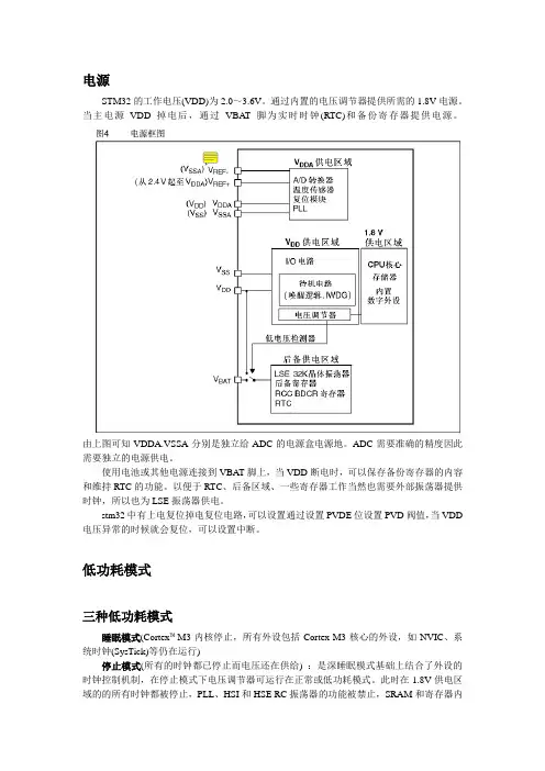
电源STM32的工作电压(VDD)为2.0~3.6V。
通过内置的电压调节器提供所需的1.8V电源。
当主电源VDD掉电后,通过VBA T脚为实时时钟(RTC)和备份寄存器提供电源。
由上图可知VDDA.VSSA分别是独立给ADC的电源盒电源地。
ADC需要准确的精度因此需要独立的电源供电。
使用电池或其他电源连接到VBAT脚上,当VDD断电时,可以保存备份寄存器的内容和维持RTC的功能。
以便于RTC、后备区域、一些寄存器工作当然也需要外部振荡器提供时钟,所以也为LSE振荡器供电。
stm32中有上电复位掉电复位电路,可以设置通过设置PVDE位设置PVD阀值,当VDD 电压异常的时候就会复位,可以设置中断。
低功耗模式三种低功耗模式睡眠模式(Cortex™-M3内核停止,所有外设包括Cortex-M3核心的外设,如NVIC、系统时钟(SysTick)等仍在运行)停止模式(所有的时钟都已停止而电压还在供给) :是深睡眠模式基础上结合了外设的时钟控制机制,在停止模式下电压调节器可运行在正常或低功耗模式。
此时在1.8V供电区域的的所有时钟都被停止,PLL、HSI和HSE RC振荡器的功能被禁止,SRAM和寄存器内容被保留下来。
在停止模式下,所有的I/O引脚都保持它们在运行模式时的状态。
待机模式(1.8V电源关闭):待机模式可实现系统的最低功耗。
该模式是在Cortex-M3深睡眠模式时关闭电压调节器。
整个1.8V供电区域被断电。
PLL、HSI和HSE振荡器也被断电。
SRAM和寄存器内容丢失。
只有备份的寄存器和待机电路维持供电。
前面是三者的详细介绍,初一看看不出有什么区别,我当时都看的晕呼呼地,做笔记时候才发现他们真正的不同。
现在讲解一下。
睡眠模式只是关掉了CM3的内核,外设都在运行包过内部外部时钟、IO口、中断NVIC 等等。
停止模式是进一步的睡眠模式它是关掉了所有的外设时钟,但是仍旧在供电。
待机模式是最低功耗的模式,它连时钟供电全部禁止除了备份的寄存器和待机电路维持供电。
STM32F20xxx_21xxx单⽚机硬件开发⼊门笔记AN3320Application noteGetting started with STM32F20xxx/21xxx MCUhardware developmentIntroductionThis application note is intended for system designers who require a hardwareimplementation overview of the development board features such as the power supply, theclock management, the reset control, the boot mode settings and the debug management. It shows how to use the high-density performance line STM32F20xxx/21xxx product familiesand describes the minimum hardware resources required to develop anSTM32F20xxx/21xxx application.Detailed reference design schematics are also contained in this document with descriptionsof the main components, interfaces and modes.August 2011Doc ID 18267 Rev 21/29/doc/20ec15b314791711cd7917a6.htmlContents AN3320Contents1Power supplies . . . . . . . . . . . . . . . . . . . . . . . . . . . . . . . . . . . . . . . . . . . . . 61.1Introduction . . . . . . . . . . . . . . . . . . . . . . . . . . . . . . . . . . . . . . . . . . . . . . . . 61.1.1Independent A/D converter supply and reference voltage . . . . . . . . . . . . 71.1.2Battery backup . . . . . . . . . . . . . . . . . . . . . . . . . . . . . . . . . . . . . . . . . . . . . 71.1.3Voltage regulator . . . . . . . . . . . . . . . . . . . . . . . . . . . . . . . . . . . . . . . . . . . 71.2Power supply schemes . . . . . . . . . . . . . . . . . . . . . . . . . . . . . . . . . . . . . . . . 81.3Reset & power supply supervisor . . . . . . . . . . . . . . . . . . . . . . . . . . . . . . . . 91.3.1Power on reset (POR) / power down reset (PDR) . . . . . . . . . . . . . . . . . . 91.3.2Programmable voltage detector (PVD) . . . . . . . . . . . . . . . . . . . . . . . . . 101.3.3System reset . . . . . . . . . . . . . . . . . . . . . . . . . . . . . . . . . . . . . . . . . . . . . 112Clocks . . . . . . . . . . . . . . . . . . . . . . . . . . . . . . . . . . . . . . . . . . . . . . . . . . . . 122.1HSE OSC clock . . . . . . . . . . . . . . . . . . . . . . . . . . . . . . . . . . . . . . . . . . . . 122.1.1External source (HSE bypass) . . . . . . . . . . . . . . . . . . . . . . . . . . . . . . . . 132.1.2External crystal/ceramic resonator (HSE crystal) . . . . . . . . . . . . . . . . . 132.2LSE OSC clock . . . . . . . . . . . . . . . . . . . . . . . . . . . . . . . . . . . . . . . . . . . . . 142.2.1External source (LSE bypass) . . . . . . . . . . . . . . . . . . . . . . . . . . . . . . . . 142.2.2External crystal/ceramic resonator (LSE crystal) . . . . . . . . . . . . . . . . . . 142.3Clock security system (CSS) . . . . . . . . . . . . . . . . . . . . . . . . . . . . . . . . . . 153Boot configuration . . . . . . . . . . . . . . . . . . . . . . . . . . . . . . . . . . . . . . . . . 163.1Boot mode selection . . . . . . . . . . . . . . . . . . . . . . . . . . . . . . . . . . . . . . . . . 163.2Boot pin connection . . . . . . . . . . . . . . . . . . . . . . . . . . . . . . . . . . . . . . . . . 163.3Embedded boot loader mode . . . . . . . . . . . . . . . . . . . . . . . . . . . . . . . . . . 174Debug management . . . . . . . . . . . . . . . . . . . . . . . . . . . . . . . . . . . . . . . . 184.1Introduction . . . . . . . . . . . . . . . . . . . . . . . . . . . . . . . . . . . . . . . . . . . . . . . 184.2SWJ debug port (serial wire and JTAG) . . . . . . . . . . . . . . . . . . . . . . . . . . 184.3Pinout and debug port pins . . . . . . . . . . . . . . . . . . . . . . . . . . . . . . . . . . . 184.3.1SWJ debug port pins . . . . . . . . . . . . . . . . . . . . . . . . . . . . . . . . . . . . . . . 184.3.2Flexible SWJ-DP pin assignment . . . . . . . . . . . . . . . . . . . . . . . . . . . . . . 194.3.3Internal pull-up and pull-down resistors on JT AG pins . . . . . . . . . . . . . . 194.3.4SWJ debug port connection with standard JTAG connector . . . . . . . . . 20 2/29 Doc ID 18267 Rev 2AN3320Contents5Recommendations . . . . . . . . . . . . . . . . . . . . . . . . . . . . . . . . . . . . . . . . . 215.1Printed circuit board . . . . . . . . . . . . . . . . . . . . . . . . . . . . . . . . . . . . . . . . . 215.2Component position . . . . . . . . . . . . . . . . . . . . . . . . . . . . . . . . . . . . . . . . . 215.3Ground and power supply (V SS, V DD) . . . . . . . . . . . . . . . . . . . . . . . . . . . 215.4Decoupling . . . . . . . . . . . . . . . . . . . . . . . . . . . . . . . . . . . . . . . . . . . . . . . . 215.5Other signals . . . . . . . . . . . . . . . . . . . . . . . . . . . . . . . . . . . . . . . . . . . . . . 225.6Unused I/Os and features . . . . . . . . . . . . . . . . . . . . . . . . . . . . . . . . . . . . 226Reference design . . . . . . . . . . . . . . . . . . . . . . . . . . . . . . . . . . . . . . . . . . 236.1Description . . . . . . . . . . . . . . . . . . . . . . . . . . . . . . . . . . . . . . . . . . . . . . . . 236.1.1Clock . . . . . . . . . . . . . . . . . . . . . . . . . . . . . . . . . . . . . . . . . . . . . . . . . . . 236.1.2Reset . . . . . . . . . . . . . . . . . . . . . . . . . . . . . . . . . . . . . . . . . . . . . . . . . . . 236.1.3Boot mode . . . . . . . . . . . . . . . . . . . . . . . . . . . . . . . . . . . . . . . . . . . . . . . 236.1.4SWJ interface . . . . . . . . . . . . . . . . . . . . . . . . . . . . . . . . . . . . . . . . . . . . . 236.1.5Power supply . . . . . . . . . . . . . . . . . . . . . . . . . . . . . . . . . . . . . . . . . . . . . 236.2Component references . . . . . . . . . . . . . . . . . . . . . . . . . . . . . . . . . . . . . . . 24 7Revision history . . . . . . . . . . . . . . . . . . . . . . . . . . . . . . . . . . . . . . . . . . . 28Doc ID 18267 Rev 23/29List of tables AN3320 List of tablesTable 1.Boot modes. . . . . . . . . . . . . . . . . . . . . . . . . . . . . . . . . . . . . . . . . . . . . . . . . . . . . . . . . . . . . 16 Table 2.Debug port pin assignment. . . . . . . . . . . . . . . . . . . . . . . . . . . . . . . . . . . . . . . . . . . . . . . . . 19 Table 3.SWJ I/O pin availability. . . . . . . . . . . . . . . . . . . . . . . . . . . . . . . . . . . . . . . . . . . . . . . . . . . . 19 Table 4.Mandatory components . . . . . . . . . . . . . . . . . . . . . . . . . . . . . . . . . . . . . . . . . . . . . . . . . . . 24 Table 5.Optional components . . . . . . . . . . . . . . . . . . . . . . . . . . . . . . . . . . . . . . . . . . . . . . . . . . . . . 24 Table 6.Reference connection for all packages. . . . . . . . . . . . . . . . . . . . . . . . . . . . . . . . . . . . . . . . 26 Table 7.Document revision history . . . . . . . . . . . . . . . . . . . . . . . . . . . . . . . . . . . . . . . . . . . . . . . . . 28 4/29 Doc ID 18267 Rev 2AN3320List of figures List of figuresFigure 1.Power supply overview. . . . . . . . . . . . . . . . . . . . . . . . . . . . . . . . . . . . . . . . . . . . . . . . . . . . . 6 Figure 2.Power supply scheme. . . . . . . . . . . . . . . . . . . . . . . . . . . . . . . . . . . . . . . . . . . . . . . . . . . . . . 9 Figure 3.Power-on reset/power-down reset waveform. . . . . . . . . . . . . . . . . . . . . . . . . . . . . . . . . . . 10 Figure 4.PVD thresholds. . . . . . . . . . . . . . . . . . . . . . . . . . . . . . . . . . . . . . . . . . . . . . . . . . . . . . . . . . 10 Figure 5.Reset circuit . . . . . . . . . . . . . . . . . . . . . . . . . . . . . . . . . . . . . . . . . . . . . . . . . . . . . . . . . . . . 11 Figure 6.HSE external clock. . . . . . . . . . . . . . . . . . . . . . . . . . . . . . . . . . . . . . . . . . . . . . . . . . . . . . . 12 Figure 7.HSE crystal/ceramic resonators. . . . . . . . . . . . . . . . . . . . . . . . . . . . . . . . . . . . . . . . . . . . . 12 Figure 8.LSE external clock . . . . . . . . . . . . . . . . . . . . . . . . . . . . . . . . . . . . . . . . . . . . . . . . . . . . . . . 14 Figure 9.LSE crystal/ceramic resonators . . . . . . . . . . . . . . . . . . . . . . . . . . . . . . . . . . . . . . . . . . . . . 14 Figure 10.Boot mode selection implementation example. . . . . . . . . . . . . . . . . . . . . . . . . . . . . . . . . . 16 Figure 11.Host-to-board connection. . . . . . . . . . . . . . . . . . . . . . . . . . . . . . . . . . . . . . . . . . . . . . . . . . 18 Figure 12.JTAG connector implementation . . . . . . . . . . . . . . . . . . . . . . . . . . . . . . . . . . . . . . . . . . . . 20 Figure 13.Typical layout for V DD/V SS pair . . . . . . . . . . . . . . . . . . . . . . . . . . . . . . . . . . . . . . . . . . . . . 22 Figure 14.STM32F207IG(H6) microcontroller reference schematic. . . . . . . . . . . . . . . . . . . . . . . . . . 25Doc ID 18267 Rev 25/29Power supplies AN33206/29 Doc ID 18267 Rev 21 Power supplies1.1 IntroductionThe device requires a 1.8V to 3.6V operating voltage supply (V DD ), excepted the WLCSPpackage witch requires 1.65V to 3.6V. An embedded regulator is used to supply the internal 1.2V digital power.The real-time clock (RTC) and backup registers can be powered from the V BAT voltage when the main V DD supply is powered off.1.V DDA and V SSA must be connected to V DD and V SS , respectively.2.The voltage on V REF ranges from 1.65V to V DDA for WLCSP64+2 packages.AN3320Power suppliesDoc ID 18267 Rev 27/291.1.1 Independent A/D converter supply and reference voltageTo improve conversion accuracy, the ADC has an independent power supply that can be filtered separately, and shielded from noise on the PCB.●the ADC voltage supply input is available on a separate V DDA pin ●an isolated supply ground connection is provided on the V SSA pinWhen available (depending on package), V REF– must be tied to V SSA .On 100-pin package and above and on WLCSP64+2To ensure a better accuracy on low-voltage inputs, the user can connect a separate external reference voltage ADC input on V REF+. The voltage on V REF+ may range from 1.8V to V DDA . On WLCSP64+2, the V REF- pin is not available, it is internally connected to the ADC ground (V SSA ).On 64-pin packagesThe V REF+ and V REF- pins are not available, they are internally connected to the ADC voltage supply (V DDA ) and ground (V SSA ).1.1.2 Battery backupTo retain the content of the Backup registers when V DD is turned off, the V BAT pin can beconnected to an optional standby voltage supplied by a battery or another source.The V BAT pin also powers the RTC unit, allowing the RTC to operate even when the main digital supply (V DD ) is turned off. The switch to the V BAT supply is controlled by the power down reset (PDR) circuitry embedded in the Reset block.If no external battery is used in the application, it is highly recommended to connect V BAT externally to V DD .1.1.3 Voltage regulatorThe voltage regulator is always enabled after reset. It works in three different modesdepending on the application modes.●in Run mode, the regulator supplies full power to the 1.2V domain (core, memories and digital peripherals)●in Stop mode, the regulator supplies low power to the 1.2V domain, preserving the contents of the registers and SRAM●in Standby mode, the regulator is powered down. The contents of the registers and SRAM are lost except for those concerned with the Standby circuitry and the Backup domain.Note:Depending on the selected package, there are specific pins that should be connected either to V SS or V DD to activate or deactivate the voltage regulator. Refer to section "Voltage regulator" in STM32F20xxx/21xxx datasheet for details .Power supplies AN33208/29 Doc ID 18267 Rev 21.2 Power supply schemesThe circuit is powered by a stabilized power supply, V DD .●Caution:–The V DD voltage range is 1.8V to 3.6V (and 1.65V to 3.6V for WLCSP64+2 package)●The V DD pins must be connected to V DD with external decoupling capacitors: one single T antalum or Ceramic capacitor (min. 4.7µF typ.10µF) for the package + one 100nF Ceramic capacitor for each V DD pin.●The V BAT pin can be connected to the external battery (1.65V < V BA T < 3.6V). If no external battery is used, it is recommended to connect this pin to V DD with a 100nF external ceramic decoupling capacitor.●The V DDA pin must be connected to two external decoupling capacitors (100nF Ceramic + 1µF Tantalum or Ceramic).●The V REF+ pin can be connected to the V DDA external power supply. If a separate, external reference voltage is applied on V REF+, a 100nF and a 1µF capacitors must be connected on this pin. In all cases, V REF+ must be kept between 1.65V and V DDA .●Additional precautions can be taken to filter analog noise:–V DDA can be connected to V DD through a ferrite bead.–The V REF+ pin can be connected to V DDA through a resistor (typ. 47Ω).●For the voltage regulator configuration, there are specific pins (REGOFF and IRROFF depending on the package) that should be connected either to VSS or VDD to activate or deactivate the voltage regulator specific. Refer to section "Voltage regulator" in STM32F20xxx/21xxx datasheet for details .●When the voltage regulator is enabled, V CAP1 and V CAP2 pins must be connected to 2*2.2µF Ceramic capacitor.AN3320Power suppliesDoc ID 18267 Rev 29/291.Optional. If a separate, external reference voltage is connected on V REF+, the two capacitors (100 nF and1µF) must be connected.2.V REF + is either connected to V REF or to V DDA .3.N is the number of V DD and V SS inputs.4.Refer to section "Voltage regulator" in STM32F20xxx/21xxx datasheet to connect REGOFF and IRROFFpins.1.3Reset & power supply supervisor1.3.1Power on reset (POR) / power down reset (PDR)The device has an integrated POR/PDR circuitry that allows proper operation starting from 1.8V .The device remains in the Reset mode as long as V DD is below a specified threshold, V POR/PDR , without the need for an external reset circuit. For more details concerning the power on/power down reset threshold, refer to the electrical characteristics in STM32F20xxx/21xxx datasheets.On WLCSP66 package if IRROFF pin is set to V DD (in that case REGOFF pin must not be activated, refer to section "Voltage regulator" in STM32F20xxx/21xxx datasheet for details ), the PDR is not functional. Then the V DD can lower below 1.8V , but the external circuitry must ensure that reset pin is activated when V DD /V DDA becomes below 1.65V .Power suppliesAN332010/29 Doc ID 18267 Rev 21.t RSTTEMPO is approximately2.6ms. V POR/PDR rising edge is 1.74V (typ.) and V POR/PDR falling edge is1.70V (typ.). Refer to STM32F20xxx/21xxx datasheets for actual value.1.3.2 Programmable voltage detector (PVD)Y ou can use the PVD to monitor the V DD power supply by comparing it to a thresholdselected by the PLS[2:0] bits in the Power control register (PWR_CR).The PVD is enabled by setting the PVDE bit.A PVDO flag is available, in the Power control/status register (PWR_CSR), to indicatewhether V DD is higher or lower than the PVD threshold. This event is internally connected to EXTI Line16 and can generatean interrupt if enabled through the EXTI registers. The PVD output interrupt can be generated when V DD drops below the PVD threshold and/or when VDD rises above the PVD threshold depending on the EXTI Line16 rising/falling edge configuration. As an example the service routine can perform emergency shutdown tasks.AN3320Power suppliesDoc ID 18267 Rev 211/291.3.3 System resetA system reset sets all registers to their reset values except for the reset flags in the clockcontroller CSR register and the registers in the Backup domain (see Figure 1).A system reset is generated when one of the following events occurs:1. A low level on the NRST pin (external reset)2. window watchdog end-of-count condition (WWDG reset)3. Independent watchdog end-of-count condition (IWDG reset)4. A software reset (SW reset)5.Low-power management resetThe reset source can be identified by checking the reset flags in the Control/Status register, RCC_CSR.The STM32F20xxx/21xxx does not require an external reset circuit to power-up correctly. Only a pull-down capacitor is recommended to improve EMS performance by protecting the device against parasitic resets. See Figure 5.Charging and discharging a pull-down capacitor through an internal resistor increases the device power consumption. The capacitor recommended value (100nF) can be reduced to 10nF to limit this power consumption;Clocks AN332012/29 Doc ID 18267 Rev 22 ClocksThree different clock sources can be used to drive the system clock (SYSCLK):●HSI oscillator clock (high-speed internal clock signal)●HSE oscillator clock (high-speed external clock signal)●PLL clockThe devices have two secondary clock sources:●32kHz low-speed internal RC (LSI RC) that drives the independent watchdog and, optionally, the RTC used for Auto-wakeup from the Stop/Standby modes.●32.768kHz low-speed external crystal (LSE crystal) that optionally drives the real-time clock (RTCCLK)Each clock source can be switched on or off independently when it is not used, to optimize the power consumption.Refer to the STM32F20xxx/21xxx reference manual RM0033 for the description of the clock tree.2.1 HSE OSC clockThe high-speed external clock signal (HSE) can be generated from two possible clock sources:●HSE external crystal/ceramic resonator (see Figure 7)●HSE user external clock (see Figure 6)1.The value of R EXT depends on the crystal characteristics. Typical value is in the range of 5 to 6 R S(resonator series resistance).2.Load capacitance C L has the following formula: C L = C L1 x C L2 / (C L1 + C L2) + C stray where: C stray is the pincapacitance and board or trace PCB-related capacitance. Typically, it is between 2pF and 7pF. Please refer to Section 5: Recommendations on page 21 to minimize its value.Figure 6.HSE external clockFigure 7.HSE crystal/ceramicAN3320ClocksDoc ID 18267 Rev 213/292.1.1 External source (HSE bypass)In this mode, an external clock source must be provided. It can have a frequency from 1 to 16MHz (refer toSTM32F20xxx/21xxx datasheets for actual max value).The external clock signal (square, sine or triangle) with a duty cycle of about 50%, has to drive the OSC_IN pin while the OSC_OUT pin must be left in the high impedance state (see Figure 7 and Figure 6).2.1.2 External crystal/ceramic resonator (HSE crystal)The external oscillator frequency ranges from 4 to 26MHz.The external oscillator has the advantage of producing a very accurate rate on the mainclock. The associated hardware configuration is shown in Figure 7. Using a 25MHz oscillator frequency is a good choice to get accurate Ethernet, USB OTG high-speed peripheral, and I 2S.The resonator and the load capacitors have to be connected as close as possible to the oscillator pins in order to minimize output distortion and startup stabilization time. The load capacitance values must be adjusted according to the selected oscillator.For C L1 and C L2 it is recommended to use high-quality ceramic capacitors in the 5pF-to-25pF range (typ.), designed for high-frequency applications and selected to meet the requirements of the crystal or resonator. C L1 and C L2, are usually the same value. Thecrystal manufacturer typically specifies a load capacitance that is the series combination of C L1 and C L2. The PCB andMCU pin capacitances must be included when sizing C L1 and C L2 (10 pF can be used as a rough estimate of the combined pin and board capacitance).Refer to the electrical characteristics sections in the datasheet of your product for more details.Clocks AN332014/29 Doc ID 18267 Rev 22.2 LSE OSC clockThe low-speed external clock signal (LSE) can be generated from two possible clocksources:●LSE external crystal/ceramic resonator (see Figure 9)●LSE user external clock (see Figure 8)1.“LSE crystal/ceramic resonators” figure:To avoid exceeding the maximum value of C L1 and C L2 (15pF) it is strongly recommended to use a resonator with a load capacitance C L ≤7pF. Never use a resonator with a load capacitance of 12.5pF.2.“LSE external clock” and “LSEcrystal/ceramic resonators” figures:OSC32_IN and OSC32_OUT pins can be used also as GPIO, but it is recommended not to use them as both RTC and GPIO pins in the same application.3.“LSE crystal/ceramic resonators” figure:The value of R EXT depends on the crystal characteristics. A 0Ω resistor would work but would not be optimal. To fine tube R S value, refer to AN2867 - Oscillator design guide for ST microcontrollers.2.2.1 External source (LSE bypass)In this mode, an external clock source must be provided. It can have a frequency of up to 1MHz. The external clock signal (square, sine or triangle) with a duty cycle of about 50% has to drive the OSC32_IN pin while the OSC32_OUT pin must be left high impedance (see Figure 8).2.2.2 External crystal/ceramic resonator (LSE crystal)The LSE crystal is a 32.768kHz low-speed external crystal or ceramic resonator. It has theadvantage of providing a low-power, but highly accurate clock source to the real-time clock peripheral (RTC) forclock/calendar or other timing functions.The resonator and the load capacitors have to be connected as close as possible to the oscillator pins in order to minimize output distortion and startup stabilization time. The load capacitance values must be adjusted according to the selected oscillator.Figure 8.LSE external clockFigure 9.LSE crystal/ceramicAN3320ClocksDoc ID 18267 Rev 215/292.3 Clock security system (CSS)The clock security system can be activated by software. In this case, the clock detector is enabled after the HSE oscillator startup delay, and disabled when this oscillator is stopped.●If a failure is detected on the HSE oscillator clock, the oscillator is automaticallydisabled. A clock failure event is sent to the break input of the TIM1 advanced control timer and an interrupt is generated to inform the software about the failure (clocksecurity system interrupt CSSI), allowing the MCU to perform rescue operations. The CSSI is linked to the Cortex?-M3 NMI (non-maskable interrupt) exception vector.●If the HSE oscillator is used directly or indirectly as the system clock (indirectly means that it is used as the PLL input clock, and the PLL clock is used as the system clock), a detected failure causes a switch of the system clock to the HSI oscillator and thedisabling of the external HSE oscillator. If the HSE oscillator clock (divided or not) is the clock entry of the PLL used as system clock when the failure occurs, the PLL is disabled too.For details, see the STM32F20xxx/21xxx (RM0033) reference manuals available from the STMicroelectronics website /doc/20ec15b314791711cd7917a6.html .Boot configuration AN332016/29 Doc ID 18267 Rev 23 Boot configuration3.1 Boot mode selectionIn the STM32F20xxx/21xxx, three different boot modes can be selected by means of theBOOT[1:0] pins as shown in Table 1.The values on the BOOT pins are latched on the 4th rising edge of SYSCLK after a reset. It is up to the user to set the BOOT1 and BOOT0 pins after reset to select the required boot mode.The BOOT pins are also resampled when exiting the Standby mode. Consequently, they must be kept in the required Boot mode configuration in the Standby mode. After this startup delay has elapsed, the CPU fetches the top-of-stack value from address 0x0000 0000, and starts code execution from the boot memory starting from 0x0000 0004.3.2 Boot pin connectionFigure 10 shows the external connection required to select the boot memory of the STM32F20xxx/21xxx.1.Resistor values are given only as a typical example.Table 1.Boot modesBOOT mode selection pinsBoot mode AliasingBOOT1BOOT0x 0Main Flash memory Main Flash memory is selected as boot space01System memory System memory is selected as boot space11Embedded SRAMEmbedded SRAM is selected as boot spaceAN3320Boot configuration3.3 Embedded boot loader modeThe Embedded boot loader mode is used to reprogram the Flash memory using one of theavailable serial USART1(PA9/PA10), USART3(PB10/11 & PC10/11), CAN2(PB5/13) or USBOTG FS(PA11/12) in Device mode (DFU: device firmware upgrade).The USART peripheral operates with the internal 16MHz oscillator (HSI). The CAN andUSB OTG FS, however, can only function if an external clock (HSE) multiple of 1 MHz(between 4 and 26 MHz)is present.This embedded boot loader is located in the System memory and is programmed by STduring production.For additional information, refer to AN2606.Doc ID 18267 Rev 217/29Debug management AN332018/29 Doc ID 18267 Rev 24 Debug management4.1 IntroductionThe Host/Target interface is the hardware equipment that connects the host to theapplication board. This interface is made of three components: a hardware debug tool, a JTAG or SW connector and a cable connecting the host to the debug tool.Figure 11 shows the connection of the host to the evaluation board STM3220G-EVAL.Figure 11.Host-to-board connection 4.2 SWJ debug port (serial wire and JTAG)The STM32F20xxx/21xxx core integrates the serial wire / JT AG debug port (SWJ-DP). It is an ARM? standard CoreSight? debug port that combines a JTAG-DP (5-pin) interface and a SW-DP (2-pin) interface.●The JTAG debug port (JTAG-DP) provides a 5-pin standard JTAG interface to the AHP-AP port●The serial wire debug port (SW-DP) provides a 2-pin (clock + data) interface to the AHP-AP portIn the SWJ-DP , the two JTAG pins of the SW-DP are multiplexed with some of the five JTAG pins of the JTAG-DP .4.3 Pinout and debug port pinsThe STM32F20xxx/21xxx MCU is offered in various packages with different numbers of available pins. As a result, some functionality related to the pin availability may differ from one package to another.4.3.1 SWJ debug port pinsFive pins are used as outputs for the SWJ-DP as alternate functions of general-purpose I/Os (GPIOs). These pins, shown in Table 2, are available on all packages.%VALUATION BOARD(OST 0#0OWER SUPPLY*4!' 37 CONNECTOR$EBUG TOOLAI BAN3320Debug managementDoc ID 18267 Rev 219/294.3.2 Flexible SWJ-DP pin assignmentAfter reset (SYSRESETn or PORESETn), all five pins used for the SWJ-DP are assigned as dedicated pins immediately usable by the debugger host (note that the trace outputs are not assigned except if explicitly programmed by the debugger host).However, some of the JTAG pins shown in Table 3 can be configured to an alternate function through the GPIOx_AFRx registers.Table 3 shows the different possibilities to release some pins.For more details, see the STM32F20xxx/21xxx (RM0033) reference manual, available from the STMicroelectronics website /doc/20ec15b314791711cd7917a6.html .4.3.3 Internal pull-up and pull-down resistors on JTAG pinsThe JTAG input pins must not be floating since they are directly connected to flip-flops to control the debug mode features. Special care must be taken with the SWCLK/TCK pin that is directly connected to the clock of some of these flip-flops. Table 2.Debug port pin assignmentSWJ-DP pin nameJTAG debug portSW debug portPinassignment TypeDescription Type Debug assignment JTMS/SWDIO I JTAG test mode selection I/O Serial wire data input/output PA13JTCK/SWCLK I JTAG test clock I Serial wire clock P A14JTDII JTAG test data input --P A15JTDO/TRACESWO O JTAG test data output -TRACESWO if async traceis enabled PB3JNTRSTIJTAG test nReset。

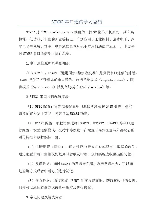
STM32串口通信学习总结STM32是STMicroelectronics推出的一款32位单片机系列,具有高性能、低功耗、丰富的外设等特点,广泛应用于工业控制、消费电子、汽车电子等领域。
其中,串口通信是单片机中常用的通信方式之一,本文将对STM32串口通信学习进行总结。
1.串口通信原理及基础知识在STM32中,USART(通用同步/异步收发器)是负责串口通信的外设。
USART提供了多种模式的串口通信,包括异步模式(Asynchronous)、同步模式(Synchronous)以及单线模式(Single-wire)等。
2.STM32串口通信配置步骤(1)GPIO配置:首先需要配置串口通信所涉及的GPIO引脚,通常需要配置为复用功能,使其具备USART功能。
(2)USART配置:根据需要选择USART1、USART2、USART3等串口进行配置,设置通信模式、波特率等参数。
在配置时需要注意与外部设备的通信标准和参数保持一致。
(3)中断配置(可选):可以选择中断方式来实现串口数据的收发。
通过配置中断,当接收到数据时会触发中断,从而实现接收数据的功能。
(4)发送数据:通过USART的发送寄存器将数据发送出去,可以通过查询方式或者中断方式进行发送。
(5)接收数据:通过读取USART的接收寄存器,获取接收到的数据。
同样可以通过查询方式或者中断方式进行接收。
3.常见问题及解决方法(1)波特率设置错误:在进行串口通信时,波特率设置错误可能会导致通信失败。
需要根据外设的要求,选择适当的波特率设置,并在STM32中进行配置。
(2)数据丢失:在高速通信或大量数据传输时,由于接收速度跟不上发送速度,可能会导致数据丢失。
可以通过增加接收缓冲区大小、优化接收中断处理等方式来解决该问题。
(3)数据帧错误:在数据传输过程中,可能发生数据位错误、校验错误等问题。
可以通过对USART的配置进行检查,包括校验位、停止位、数据位等的设置是否正确。
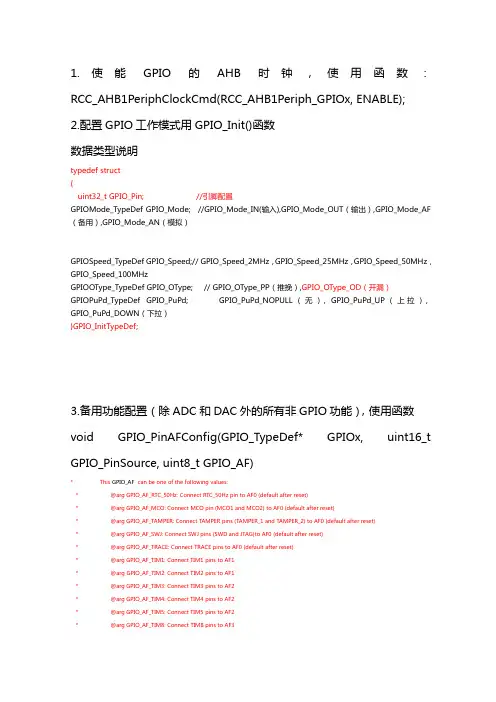
1.使能GPIO的AHB时钟,使用函数:RCC_AHB1PeriphClockCmd(RCC_AHB1Periph_GPIOx, ENABLE);2.配置GPIO工作模式用GPIO_Init()函数数据类型说明typedef struct{uint32_t GPIO_Pin; //引脚配置GPIOMode_TypeDef GPIO_Mode; //GPIO_Mode_IN(输入),GPIO_Mode_OUT(输出),GPIO_Mode_AF (备用),GPIO_Mode_AN(模拟)GPIOSpeed_TypeDef GPIO_Speed;// GPIO_Speed_2MHz,GPIO_Speed_25MHz,GPIO_Speed_50MHz,GPIO_Speed_100MHzGPIOOType_TypeDef GPIO_OType; // GPIO_OType_PP(推挽),GPIO_OType_OD(开漏)GPIOPuPd_TypeDef GPIO_PuPd; GPIO_PuPd_NOPULL(无),GPIO_PuPd_UP(上拉),GPIO_PuPd_DOWN(下拉)}GPIO_InitTypeDef;3.备用功能配置(除ADC和DAC外的所有非GPIO功能),使用函数void GPIO_PinAFConfig(GPIO_TypeDef* GPIOx, uint16_t GPIO_PinSource, uint8_t GPIO_AF)* This GPIO_AF can be one of the following values:* @arg GPIO_AF_RTC_50Hz: Connect RTC_50Hz pin to AF0 (default after reset)* @arg GPIO_AF_MCO: Connect MCO pin (MCO1 and MCO2) to AF0 (default after reset)* @arg GPIO_AF_TAMPER: Connect TAMPER pins (TAMPER_1 and TAMPER_2) to AF0 (default after reset)* @arg GPIO_AF_SWJ: Connect SWJ pins (SWD and JTAG)to AF0 (default after reset)* @arg GPIO_AF_TRACE: Connect TRACE pins to AF0 (default after reset)* @arg GPIO_AF_TIM1: Connect TIM1 pins to AF1* @arg GPIO_AF_TIM2: Connect TIM2 pins to AF1* @arg GPIO_AF_TIM3: Connect TIM3 pins to AF2* @arg GPIO_AF_TIM4: Connect TIM4 pins to AF2* @arg GPIO_AF_TIM5: Connect TIM5 pins to AF2* @arg GPIO_AF_TIM8: Connect TIM8 pins to AF3* @arg GPIO_AF_TIM9: Connect TIM9 pins to AF3* @arg GPIO_AF_TIM10: Connect TIM10 pins to AF3* @arg GPIO_AF_TIM11: Connect TIM11 pins to AF3* @arg GPIO_AF_I2C1: Connect I2C1 pins to AF4* @arg GPIO_AF_I2C2: Connect I2C2 pins to AF4* @arg GPIO_AF_I2C3: Connect I2C3 pins to AF4* @arg GPIO_AF_SPI1: Connect SPI1 pins to AF5* @arg GPIO_AF_SPI2: Connect SPI2/I2S2 pins to AF5* @arg GPIO_AF_SPI3: Connect SPI3/I2S3 pins to AF6* @arg GPIO_AF_I2S3ext: Connect I2S3ext pins to AF7* @arg GPIO_AF_USART1: Connect USART1 pins to AF7* @arg GPIO_AF_USART2: Connect USART2 pins to AF7* @arg GPIO_AF_USART3: Connect USART3 pins to AF7* @arg GPIO_AF_UART4: Connect UART4 pins to AF8* @arg GPIO_AF_UART5: Connect UART5 pins to AF8* @arg GPIO_AF_USART6: Connect USART6 pins to AF8* @arg GPIO_AF_CAN1: Connect CAN1 pins to AF9* @arg GPIO_AF_CAN2: Connect CAN2 pins to AF9* @arg GPIO_AF_TIM12: Connect TIM12 pins to AF9* @arg GPIO_AF_TIM13: Connect TIM13 pins to AF9* @arg GPIO_AF_TIM14: Connect TIM14 pins to AF9* @arg GPIO_AF_OTG_FS: Connect OTG_FS pins to AF10* @arg GPIO_AF_OTG_HS: Connect OTG_HS pins to AF10* @arg GPIO_AF_ETH: Connect ETHERNET pins to AF11* @arg GPIO_AF_FSMC: Connect FSMC pins to AF12* @arg GPIO_AF_OTG_HS_FS: Connect OTG HS (configured in FS) pins to AF12* @arg GPIO_AF_SDIO: Connect SDIO pins to AF12* @arg GPIO_AF_DCMI: Connect DCMI pins to AF13* @arg GPIO_AF_EVENTOUT: Connect EVENTOUT pins to AF154.使用GPIO_ReadInputData(GPIO_TypeDef* GPIOx)和GPIO_ReadInputDataBit(GPIO_TypeDef* GPIOx, uint16_t GPIO_Pin)读输入信号5.使用GPIO_SetBits()/GPIO_ResetBits()设置输出引脚6.上电或复位后,引脚备用功能都没启用(JTAG引脚除外),为悬浮输入状态7.LSE引脚OSC32_IN 和OSC32_OUT(PC14 and PC15)的优先级高于GPIO8.HSE引脚OSC_IN/OSC_OUT (PH0 / PH1)的优先级高于GPIO例程:int main(void){GPIO_InitTypeDef GPIO_InitStructure;/* GPIOG Periph clock enable */RCC_AHB1PeriphClockCmd(RCC_AHB1Periph_GPIOD, ENABLE);RCC_AHB1PeriphClockCmd(RCC_AHB1Periph_GPIOA, ENABLE);GPIO_InitStructure.GPIO_Pin = GPIO_Pin_12 | GPIO_Pin_13;GPIO_InitStructure.GPIO_Mode = GPIO_Mode_OUT;GPIO_InitStructure.GPIO_OType = GPIO_OType_PP;GPIO_InitStructure.GPIO_Speed = GPIO_Speed_100MHz;GPIO_InitStructure.GPIO_PuPd = GPIO_PuPd_NOPULL;GPIO_Init(GPIOD, &GPIO_InitStructure);GPIO_InitStructure.GPIO_Pin = GPIO_Pin_0;GPIO_InitStructure.GPIO_Mode = GPIO_Mode_IN;GPIO_InitStructure.GPIO_PuPd = GPIO_PuPd_NOPULL;GPIO_Init(GPIOA,&GPIO_InitStructure);GPIO_SetBits(GPIOD, GPIO_Pin_12);GPIO_ResetBits(GPIOD, GPIO_Pin_13);while (1){if(GPIO_ReadInputDataBit(GPIOA,GPIO_Pin_0)==0){GPIO_SetBits(GPIOD, GPIO_Pin_13);GPIO_ResetBits(GPIOD, GPIO_Pin_12);}else{GPIO_SetBits(GPIOD, GPIO_Pin_12); GPIO_ResetBits(GPIOD, GPIO_Pin_13);}}}。
推挽输出与开漏输出的区别推挽输出推挽输出::可以输出高可以输出高,,低电平低电平,,连接数字器件连接数字器件; ;开漏输出开漏输出::输出端相当于三极管的集电极输出端相当于三极管的集电极. . 要得到高电平状态需要上拉电阻才行要得到高电平状态需要上拉电阻才行. . 适合于做电流型的驱动电流型的驱动,,其吸收电流的能力相对强其吸收电流的能力相对强((一般20ma 以内以内). ).推挽结构一般是指两个三极管分别受两互补信号的控制推挽结构一般是指两个三极管分别受两互补信号的控制,,总是在一个三极管导通的时候另一个截止另一个截止. .要实现“线与”需要用OC(open collector)collector)门电路门电路门电路..是两个参数相同的三极管或MOSFET,以推挽方式存在于电路中以推挽方式存在于电路中,,各负责正负半周的波形放大任务各负责正负半周的波形放大任务,,电路工作时,两只对称的功率开关管每次只有一个导通,所以导通损耗小关管每次只有一个导通,所以导通损耗小,,效率高。
输出既可以向负载灌电流,也可以从负载抽取电流。
抽取电流。
问题:问题:很多芯片的供电电压不一样,有3.3v 和5.0v 5.0v,需要把几种,需要把几种IC 的不同口连接在一起,是不是直接连接就可以了?实际上系统是应用在I2C 上面。
上面。
简答:简答:1、部分3.3V 器件有5V 兼容性,可以利用这种容性直接连接兼容性,可以利用这种容性直接连接2、应用电压转换器件,如TPS76733就是5V 输入,转换成3.3V 3.3V、、1A 输出。
输出。
开漏电路特点及应用在电路设计时我们常常遇到开漏(在电路设计时我们常常遇到开漏(open drain open drain )和开集()和开集()和开集(open collector open collector )的概念。
所)的概念。
所谓开漏电路概念中提到的“漏”就是指MOSFET 的漏极。
STM32中C语言知识点初学者必看1. 数据类型:在C语言中,常用的数据类型包括整型(如int、long)、浮点型(如float、double)、字符型(如char),以及指针类型等。
2.变量和常量:变量是用来存储数据的,而常量是固定的数值,不可修改。
3. 运算符:C语言提供了一系列的运算符,包括算术运算符(如+、-、*、/),关系运算符(如<、>、==、!=),逻辑运算符(如&&,!),位运算符(如&,^),赋值运算符(如=、+=、-=),以及其他一些特殊的运算符(如sizeof、?:)等。
4. 控制语句:C语言提供了若干种控制语句,包括条件语句(如if、switch),循环语句(如for、while、do-while),以及跳转语句(如break、continue、goto)等。
5.数组:数组是一种用于存储相同类型数据的结构,可以通过下标来访问数组中的元素。
6.字符串:字符串是由字符组成的数组,在C语言中,字符串以'\0'结尾。
7.函数:函数是一段具有特定功能的代码块,可以通过函数调用来执行。
C语言中,函数有返回值和无返回值的两种类型。
8.结构体:结构体是一种自定义的数据类型,可以包含多个不同类型的成员变量。
9.指针:指针是用来存储内存地址的变量,可以通过指针来访问和修改内存中的数据。
10.文件操作:C语言提供了一系列的文件操作函数,可以对文件进行读写操作。
11.预处理器:C语言中的预处理器指令以#开头,用于在程序编译之前进行一些预处理操作,如宏定义、条件编译等。
12. 头文件和库:头文件是包含一些函数和变量声明的文件,可以通过#include指令引用。
库文件是包含一些函数和变量实现的文件,可以通过链接库来使用其中的函数和变量。
13. 内存管理:C语言中可以通过动态内存分配函数(如malloc、free)来管理内存的分配和释放。
14. 异常处理:C语言中没有内置的异常处理机制,但可以通过返回错误码或使用setjmp和longjmp来实现简单的异常处理。
STM32系统结构STM32f10xxx系统结构内核IP从结构框图上看,Cortex-M3内部有若干个总线接口,以使CM3能同时取址和访内(访问内存),它们是:指令存储区总线(两条)、系统总线、私有外设总线。
有两条代码存储区总线负责对代码存储区(即 FLASH 外设)的访问,分别是 I-Code 总线和 D-Code 总线。
I-Code用于取指,D-Code用于查表等操作,它们按最佳执行速度进行优化。
系统总线(System)用于访问内存和外设,覆盖的区域包括SRAM,片上外设,片外RAM,片外扩展设备,以及系统级存储区的部分空间。
私有外设总线负责一部分私有外设的访问,主要就是访问调试组件。
它们也在系统级存储区。
还有一个DMA总线,从字面上看,DMA是data memory access的意思,是一种连接内核和外设的桥梁,它可以访问外设、内存,传输不受CPU的控制,并且是双向通信。
简而言之,这个家伙就是一个速度很快的且不受老大控制的数据搬运工。
处理器外设(内核之外的外设)从结构框图上看,STM32的外设有串口、定时器、IO口、FSMC、SDIO、SPI、I2C等,这些外设按照速度的不同,分别挂载到AHB、APB2、APB1这三条总线上。
寄存器什么是寄存器?寄存器是内置于各个IP外设中,是一种用于配置外设功能的存储器,并且有想对应的地址。
一切库的封装始于映射。
是不是看的眼都花了,如果进行寄存器开发,就需要怼地址以及对寄存器进行字节赋值,不仅效率低而且容易出错。
库的存在就是为了解决这类问题,将代码语义化。
语义化思想不仅仅是嵌入式有的,前端代码也在追求语义特性。
从点灯开始学习STM32内核库文件分析cor_cm3.h这个头文件实现了:1、内核结构体寄存器定义。
2、内核寄存器内存映射。
3、内存寄存器位定义。
跟处理器相关的头文件stm32f10x.h实现的功能一样,一个是针对内核的寄存器,一个是针对内核之外,即处理器的寄存器。
STM32 自学笔记(三)一、USART 简介 USAR T 的 使 用TD_Simon 2013/03/22 STM32 最多可提供 5 路串口,STM32F103RBT6,只有 3 个串口串口最基本的设置, 就是波特率的设置。
STM32 的串口使用起来还是蛮简单的,只要开启了串口时钟,并设 置相应 IO 口的模式,然后配置一下波特率,数据位长度,奇偶校验位等信息,就可以 使用了。
二、USART 的使用设置 1. NVIC_InitTypeDef NVIC_InitStructure; 的结构体 //定义 NVIC_InitTypeDef 型2. RCC_APB2PeriphClockCmd(RCC_APB2Periph_USART1|RCC_APB2Periph_GPIOA| RCC_APB2Periph_AFIO, ENABLE); //使能串口时钟、GPIO 时钟、端口复用时钟 3. 发送 TXD 端口设置,需设置为复用推挽输出 GPIO_Mode_AF_PP ; 4. NVIC 配置中断通道 NVIC_IRQChannel、中断抢占优先级 NVIC_IRQChannelPreemptionPriority、 中断子优先级 NVIC_IRQChannelSubPriority,IRQ 通道使能 NVIC_InitStructure.NVIC_IRQChannelCmd = ENABLE; 5. USART 初始化设置 (1) 波特率设置 9600; USART_InitStructure.USART_BaudRate = bound;//一般设置为 接收 RXD 端口初始化,需设置为浮空输入模式 GPIO_Mode_FLOATIG。
(2) 数据为长度设置(一个帧中传输或者接收到的数据位数) USART_InitStructure.USART_WordLength = USART_WordLength_8b; (3) 设置发送的停止位数目 USART_InitStructure.USART_StopBits = USART_StopBits_1; (4) 奇偶模式设置 USART_Parity_NO:奇偶失能 USART_Parity_Odd:奇校验 USART_Parity_Even:偶校验 例如: USART_InitStructure.USART_Parity = USART_Parity_No; STM32 自学笔记(三) TD_Simon 2013/03/22(5) 硬件流控制 USART_HardwareFlowControl_None 失能 USART_HardwareFlowControl_RTS 发送请求 RTS 使能 USART_HardwareFlowControl_CTS 清除发送 CTS 使能 USART_HardwareFlowControl_RTS_CTS RTS 和 CTS 使能.例如: SART_InitStructure.USART_HardwareFlowControl = USART_HardwareFlowControl_None; (6) 指定使能或失能发送和接收模式 USART_InitStructure.USART_Mode = USART_Mode_Rx | USART_Mode_Tx; (7) 根据 USART_InitStruct 中指定的参数初始化外设 USARTx 寄存器 USART_Init(USART1, &USART_InitStructure); (8) 使能或者失能指定的 USART 中断 USART_ITConfig(USART1, USART_IT_RXNE, ENABLE); //参数 2 为待使能的中断源 (9) 使能或者失能 USART 外设 6. 编写串口服务子程序 void USART1_IRQHandler(void) { } USART_Cmd(USART1, ENABLE); 发现错误请联系我QQ:859054503。
STM32学前班教程之一:为什么是它经过几天的学习,基本掌握了STM32的调试环境和一些基本知识。
想拿出来与大家共享,笨教程本着最大限度简化删减STM32入门的过程的思想,会把我的整个入门前的工作推荐给大家。
就算是给网上的众多教程、笔记的一种补充吧,所以叫学前班教程。
其中涉及产品一律隐去来源和品牌,以防广告之嫌。
全部汉字内容为个人笔记。
所有相关参考资料也全部列出。
:lol教程会分几篇,因为太长啦。
今天先来说说为什么是它——我选择STM32的原因。
我对未来的规划是以功能性为主的,在功能和面积之间做以平衡是我的首要选择,而把运算放在第二位,这根我的专业有关系。
里面的运算其实并不复杂,在入门阶段想尽量减少所接触的东西。
不过说实话,对DSP的外设并和开发环境不满意,这是为什么STM32一出就转向的原因。
下面是我自己做过的两块DSP28的全功能最小系统板,在做这两块板子的过程中发现要想尽力缩小DSP的面积实在不容易(目前只能达到50mm×45mm,这还是没有其他器件的情况下),尤其是双电源的供电方式和1.9V的电源让人很头疼。
后来因为一个项目,接触了LPC2148并做了一块板子,发现小型的ARM7在外设够用的情况下其实很不错,于是开始搜集相关芯片资料,也同时对小面积的AVR和51都进行了大致的比较,这个时候发现了CortexM3的STM32,比2148拥有更丰富和灵活的外设,性能几乎是2148两倍(按照MIPS值计算)。
正好2148我还没上手,就直接转了这款STM32F103。
与2811相比较(核心1.8V供电情况下),135MHz×1MIPS。
现在用STM32F103,72MHz×1.25MIPS,性能是DSP的66%,STM32F103R型(64管脚)芯片面积只有2811的51%,STM32F103C型(48管脚)面积是2811的25%,最大功耗是DSP的20%,单片价格是DSP的30%。