版图寄生参数提取技术的研究
- 格式:pdf
- 大小:1.87 MB
- 文档页数:70
寄生参数提取 starrc流程英文回答:## Parasitic Parameter Extraction (StarRC Flow)。
Introduction.Parasitic parameters are key factors influencing the accuracy and efficiency of modern integrated circuit (IC) designs. These parameters account for the unwantedelectrical effects caused by the physical layout of transistors and interconnects, and their accurateextraction is crucial for predicting circuit performance and reliability.StarRC is a widely used commercial tool for parasitic parameter extraction. It employs a full-wave electromagnetic field solver to compute the resistance, capacitance, and inductance of various structures within an IC layout. This approach provides highly accurate resultsbut can be computationally intensive for large and complex designs.StarRC Extraction Flow.The StarRC parasitic parameter extraction flowtypically involves the following steps:1. Layout Preparation: The IC layout is prepared by flattening the layers and removing unnecessary details.2. Mesh Generation: A mesh is generated over the layout to define the geometry for electromagnetic field simulations.3. Electromagnetic Field Simulation: The full-wave solver in StarRC is employed to compute the electromagnetic fields and extract the parasitic parameters.4. Post-Processing: The extracted parasitic parameters are post-processed to remove unwanted effects and improve the accuracy of the extraction.Applications of Parasitic Parameter Extraction.The parasitic parameters extracted using StarRC can be utilized in various applications, including:Circuit simulation: Parasitic parameters can be incorporated into circuit simulators to predict circuit behavior under different operating conditions.Timing analysis: Parasitic parameters impact circuit delays and timing characteristics, and their accurate extraction is essential for accurate timing analysis.Electrostatic discharge (ESD) analysis: Parasitic parameters influence the ESD susceptibility of ICs, and their extraction is crucial for ESD protection design.Power integrity analysis: Parasitic parameters affect power distribution networks and can lead to power supply noise and voltage drop issues, which can be mitigated by considering these parameters in power integrity analysis.Benefits of Using StarRC.StarRC offers several advantages for parasitic parameter extraction:Accuracy: StarRC employs a full-wave electromagnetic field solver, which provides highly accurate results.Scalability: StarRC can handle large and complex designs with millions of transistors and billions of interconnects.Efficiency: StarRC utilizes advanced algorithms and parallelization techniques to optimize the extraction process.User-Friendliness: StarRC provides a user-friendly interface and comprehensive documentation to facilitate its usage.Conclusion.Parasitic parameter extraction is critical for modern IC design. StarRC offers a robust and accurate solution for extracting these parameters, enabling designers to better predict circuit performance, improve reliability, and mitigate design risks.中文回答:## 寄生参数提取(StarRC 流程)。
版图设计中的寄生参数分析1.引言正如我们了解的,工艺层是芯片设计的重要组成部分。
一层金属搭在另一层金属上面,一个晶体管靠近另一个晶体管放置,而且这些晶体管全部都是在衬底上制作的。
只要在工艺制造中引入了两种不同的工艺层,就会产生相应的寄生器件,这些寄生器件广泛地分布在芯片各处,更糟糕的是我们无法摆脱它们。
寄生器件是我们非常不希望出现的,它会降低电路的速度,改变频率响应或者一些意想不到的事情发生。
既然寄生是无法避免的,那么电路设计者就要充分将这些因素考虑进去,尽量留一些余量以便把寄生参数带来的影响降至最低。
2.寄生参数的种类寄生参数主要包括了电容寄生、电阻寄生,和电感寄生。
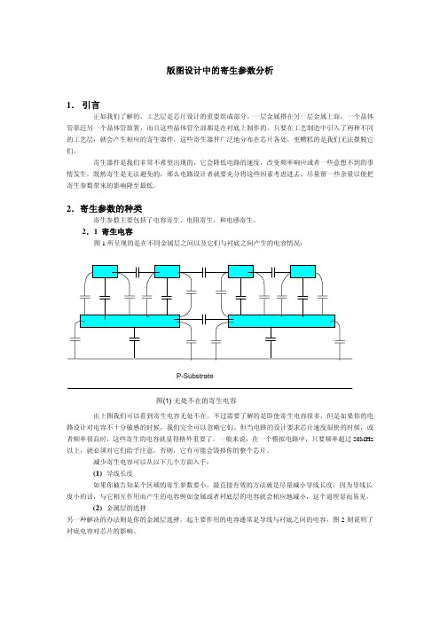
2.1 寄生电容图1所呈现的是在不同金属层之间以及它们与衬底之间产生的电容情况:图(1) 无处不在的寄生电容由上图我们可以看到寄生电容无处不在。
不过需要了解的是即使寄生电容很多,但是如果你的电路设计对电容不十分敏感的时候,我们完全可以忽略它们。
但当电路的设计要求芯片速度很快的时候,或者频率很高时,这些寄生的电容就显得格外重要了。
一般来说,在一个模拟电路中,只要频率超过20MHz 以上,就必须对它们给予注意,否则,它有可能会毁掉你的整个芯片。
减少寄生电容可以从以下几个方面入手:(1)导线长度如果你被告知某个区域的寄生参数要小,最直接有效的方法就是尽量减小导线长度,因为导线长度小的话,与它相互作用而产生的电容例如金属或者衬底层的电容就会相应地减小,这个道理显而易见。
(2)金属层的选择另一种解决的办法则是你的金属层选择。
起主要作用的电容通常是导线与衬底之间的电容,图2则说明了衬底电容对芯片的影响。
Noisy Quiet图(2) 衬底电容产生的噪声影响如上所示,电路1和电路2都对地产生了一个衬底电容,衬底本身又有一个寄生电阻,这样一来电路1的噪声就通过衬底耦合到电路2上面,这是我们不希望看到的。
(设法使所有的噪声都远离衬底)因此我们改变一下金属层,通常情况下,最高金属层所形成的电容总是最小的。

OverviewSynopsys’ Star-RCXT™ is the electronic design automation (EDA) industry’s gold standard for parasitic extraction. It provides a single solution for ASIC, system-on-chip (SoC), digital custom,memory and analog designs. Trusted by over 250 semiconductor companies and proven in thousands of production designs, Star-RCXT delivers fast and sub-femtofarad accurate technology. The Star-RCXT solution offers advanced capabilities needed for sub-65-nanometer (nm) designs, including variation-aware parasitic extraction, chemical-mechanical polishing (CMP) based and litho-aware extraction, inductance extraction and analog mixed signal design flow. Its seamless integration with industry leading physical verification, circuit simulation, timing, signal integrity, power, reliability and RTL2GDSII flows enables unmatched ease-of-use, increased productivity and reduced time-to-market. Star-RCXT is used by leading foundries to solve process modeling challenges at 65-nm and 45-nm.Star-RCXT™Parasitic extractionStar-RCXT Parasitic Extraction SolutionSemiconductor process technology has been continually scaling down for the past four decades and the trend continues. In the early days of integrated circuits (ICs), the speed bottleneck was at the circuit level, whereas interconnects were treated as ideal connections with the parasitic effects ignored. With shrinking process technologies, increasing die size and clock frequency, interconnect parasitic effects have begun to manifest themselves in signal delay and noise. Consequently, interconnects now play an important role in the design flow. Today, IC design is interconnect-limited and the design flow is interconnect-driven. A trusted parasitic extraction tool that models advanced process effects and has the capacity to handle large designs with tens of millions of transistors and cells is required to enable designers to quickly achieve their sign-off goals.Star-RCXT has the capacity and accuracy for sign-off extraction on the world’s largest SoC designs. Star-RCXT’s proprietary, advanced technology extracts full-chip designs extremely fast and provides accurate results within 5 percent or 0.2 femto-farad of industry-standard field solvers. Star-RCXT achieves its high accuracy by performing detailed modeling of every capacitive interaction. While, other extraction tools attempt to increase speed by modeling only a subset of the capacitive interactions, Star-RCXT extracts billions of capacitors for a typical design and by using a proprietary parasitic reduction capability, generates the smallest possible netlist, to achieve accurate results. Figure 2 shows excellent correlation between Star-RCXT and Raphael-NXT and demonstrates the accuracy of Star-RCXT.Star-RCXT provides parasitic extraction solution for full-chip gate-level implementation and sign-off as well as for transistor-level custom, memory, analog-mixed-signal (AMS) and radio-frequency (RF) designers, as shown in Figure 1.Gate-level ExtractionStar-RCXT is easily integrated into all industry standard design flows – Synopsys’ Galaxy™ Design Platform, and other third party implementation platforms – using Synopsys’ Milkyway™, LEF/DEF or GDSII interfaces. Galaxy users benefit from the increased productivity of Milkyway as well as the integration and faster convergence and flexibility of full-chip extraction at any time during the design cycle. In addition, Star-RCXT’s tight binary interface with PrimeTime®, PrimeTime SI, PrimeTime PX and integration with PrimeRail enables accurate post-layout optimization and timing, noise and power network sign-off.Transistor-level ExtractionStar-RCXT is integrated with the EDA industry’s leading layout-versus-schematic verification tools and simulation tools – Hercules™, Calibre, HSIM plus, NanoSim™ , HSPICE® and NanoTime for high-seed productive design. Star-RCXT also reads connectivity, cross-reference, and device information from a generated data-base and integrates with third-party analysis tools through industry standard SPICE, DSPF and SPEF netlist formats. For the highest throughput, Star-RCXT offers hierarchical and in-context modes of extraction.Virtuoso Custom Design Platform IntegrationStar-RCXT is integrated with Virtuoso® Analog Design Environment (ADE) for AMS and RF design. Star-RCXT generates Design Framework II (DFII) database parasitic views for netlisting and simulation, compatible with common netlisting interfaces used within ADE. A probing utility is also providedto probe parasitics either within the parasitic view or within the matching schematic view. The parasitic prober also provides the ability to output probed parasitics to an ASCII report file, and to annotate parasitic view total capacitance values to an associated schematic view.Reluctance (Inductance) ExtractionInductance effect becomes more and more prominent as the resistance (both device and interconnect) decreases andthe operating frequency increases. At low frequencies, RC modeling is sufficient and inductance can safely be ignored.As clock frequencies increase, however, modeling global interconnects such as RC circuits are no longer adequate and inductance must be included in the modeling. Ignoring the inductance effect can underestimate signal integrity problems as well.Star-RCXT provides a novel approach to modeling on-chip inductance effects, called partial reluctance extraction. Reluc-tance is defined as the inverse of inductance. Reluctance effects are localized just like capacitance and unlike inductance, resulting in a much sparser matrix compared to inductance. This enables Star-RCXT to produce the smallest netlist without losing any accuracy – overall achieving orders of magnitude faster extraction and simulation.Variation-aware extractionWith shrinking technology, parametric yield due to variationsin critical device and interconnect process parameters has become the dominant factor in yield loss. In order to improve silicon predictability it is mandatory that extraction tools model the process variation accurately. Also, as the uncertainty grows,Figure 1: Star-RCXT provides comprehensive solution for gate-level and transistor-level extractionthe traditional corner-based methodologies requiring multiple process technology files and time-consuming multiple extraction and simulation runs are becoming impractical. Statistical techniques are needed to model these process variation effects. Star-RCXT offers advanced statistical solution that enables sensitivity based parasitic extraction for interconnect process and temperature variation-aware designs at 65-nm and beyond. The variation of each process parameter, such as conductor or dielectric thickness, is available through the variation-aware process technology file and is used to compute sensitivities of parasitic values based on each of the process variations. Star-RCXT’s sensitivity-based extraction solution offers unique benefits to traditional STA flow users as well as to the variation-aware STA flow users, as shown in figure . It enhances the productivity of the traditional flow designers by eliminating the need to do multiple corner extractions, instead providing a single run sensitivity based extraction and multiple netlisting to feed into the traditional analysis – overall, providing 2X faster solution than traditional 5-corner extraction. On the other hand, for variation-aware STA, it generates a single sensitivity-based netlist for fast and robust sign-off. Star-RCXT Key FeaturesComprehensive Process Modeling Conformal dielectric process support Support of Air Gap Via cap extraction Layer ETCHNonlinear RPSQ variation in function of Silicon width Temperature dependent resistance modeling for conducting layers and vias••••••Support of background dielectric Nonlinear via resistance modeling 45-degree routing supportSupport of multiple inter-layer dielectric Support of multiple intra-layer dielectric Support for co-vertical conductors Support for non-planarized metalMultiple cap accuracy mode for different technology (MODE100/MODE200/MODE400) Advanced Process Modeling Sensitivity Extraction CMP simulator interface Litho-aware extractionSingle run multi-corner extraction Reluctance extraction Substrate extractionAccurate D interconnect modelingWidth and Spacing dependent Thickness variation Bottom Thickness variation Density-based thickness variation Multiple density-based variationWidth and Spacing dependent RPSQ variation RPSQ variation in function of Silicon width Nonlinear RPSQ variation Trapezoidal polygon support Dielectric damage modeling Automatic Field Solver FlowCopper interconnect, local interconnect modeling Low-K dielectric, silicon on insulator (SOI) modeling•••••••••••••••••••••••••••Over 99% of nets within 5% or 200aF-10%-5%0%5%10%N u m b e r o f N e t s50100150200250Percentage ErrorFigure 2: Star-RCXT is strongly correlated with Raphael-NXT (field solver)Figure 3: Star-RCXT’s sensitivity based extraction solution supports traditional corner-based and variation-aware STA and simulation flowsGate-level Flow Gray-Box ExtractionDirect interface with Milkyway Database Direct interface with LEF/DEF 5.6Flexibility of Instance port handling Reading of gzip compressed LEF/DEF files Reduction of netlist sizeSupport metal fill polygons from GDSII file.Support GDS inputs for LEF macros.Support hierarchical LEF/DEF inputs.Power net extraction Transistor-level FlowFlexibility of cap threshold handling Resistance threshold handlingAbility to add probe texts to the final netlist Support coupling capacitance to bulk layersSupport all device types including user-defined devices and generic devicesInterface to Hercules physical verificationInterface to Calibre physical verification through CCI Flexibility to control netlist type Support multiple cross-reference flowFlexibility of ignoring the parameter parasitic presented in spice modelSupport parasitic with model namesAbility to extract device of shrunk design parasitic for actual drawn design••••••••••••••••••••••Productivity and Ease of Use Incremental Extraction Distributed Processing License Queuing ADE integration Hierarchical Extraction Selective net extractionSupport of multiple netlist formats (SBPF/SPF/SPEF) Ability to control a number of characters in a line of netlist Ability to write device parameter in parasitic netlist Ability to split power net parasitic into a separate netlist Ability to extract device parameters such as width/length and report in parasitic netlistAbility to output original design coordinates of instance.Ability to extract a design in a given temperature Ability to read time capacitance or designed cap during extractionAbility to extract multiple corners simultaneously Ability to merge multiple extraction result to one file Flexibility to control of ground capacitanceAbility to write parasitic diode to parasitic capacitance User-control reduction of parasitic netlists Multiple reduction mode for different application Validated silicon models available from leading foundries including TSMC, UMC, Chartered•••••••••••••••••••••Synopsys, Inc.700 East Middlefield Road Mountain View, CA 9404 Specifications File Format SupportStar-RCXT supports the following industry-standard formats and interfaces:Layout data in: GDSII, LEF/DEF, Milkyway, Hercules,CalibreOutput formats: DSPF, SPICE, SPEF, SSPEF Binary interface: Direct binary interface to PrimeTime SI System RequirementsDRAM: 512MB, recommend 1GB Swap Space: 512MB, recommend 2GBInstallation disk space: 250MB baseline plus 250MB per platformDesign disk space depends on the circuit size, recommended minimum 500MB•••••••For more information about this product, sales, support services or training, please contact your local Synopsys representative or call 1-800-388-9125.。

西安邮电大学集成电路版图设计实验报告学号:XXX姓名:XX班级:微电子XX日期:20XX目录实验一、反相器电路的版图验证1)反相器电路2)反相器电路前仿真3)反相器电路版图说明4)反相器电路版图DRC验证5)反相器电路版图LVS验证6)反相器电路版图提取寄生参数7)反相器电路版图后仿真8)小结实验二、电阻负载共源放大器版图验证9)电阻负载共源放大器电路10)电阻负载共源放大器电路前仿真11)电阻负载共源放大器电路版图说明12)电阻负载共源放大器电路版图DRC验证13)电阻负载共源放大器电路版图LVS验证14)电阻负载共源放大器电路版图提取寄生参数15)电阻负载共源放大器电路版图后仿真16)小结实验一、反相器电路的版图验证1、反相器电路反相器电路由一个PMOS、NPOS管,输入输出端、地、电源端和SUB 端构成,其中VDD接PMOS管源端和衬底,地接NMOS管的漏端,输入端接两MOS管栅极,输出端接两MOS管漏端,SUB端单独引出,搭建好的反相器电路如图1所示。
图1 反相器原理图2、反相器电路前仿真通过工具栏的Design-Create Cellview-From Cellview将反相器电路转化为symbol,和schemetic保存在相同的cell中。
然后重新创建一个cell,插入之前创建好的反相器symbol,插入电感、电容、信号源、地等搭建一个前仿真电路,此处最好在输入输出网络上打上text,以便显示波形时方便观察,如图2所示。
图2 前仿真电路图反相器的输入端设置为方波信号,设置合适的高低电平、脉冲周期、上升时间、下降时间,将频率设置为参数变量F,选择瞬态分析,设置变量值为100KHZ,仿真时间为20u,然后进行仿真,如果仿真结果很密集而不清晰可以右键框选图形放大,如图3所示。
图3 前仿真结果3、反相器电路版图说明打开之前搭建好的反相器电路,通过Tools-Design Synthesis-Laout XL新建一个同cell目录下的Laout文件,在原理图上选中两个MOS管后在Laout中选择Create-Pick From Schematic从原理图中调入两个器件的版图模型。

使用Calibre xRC实现RFCMOS电路的寄生参量提取及后仿真郭慧民[摘要]Calibre xRC是Mentor Graphics公司用于寄生参量提取的工具,其强大的功能和良好的易用性使其得到业界的广泛认可。
本文以采用RFCMOS工艺实现的LNA为例,介绍使用Calibre xRC对RFCMOS电路寄生参量提取,以Calibreview 形式输出以及在Virtuoso的ADE中直接后仿真的流程。
本文还将讨论Calibre xRC特有的XCELL方式对包含RF器件的电路仿真结果的影响。
采用Calibre xRC提取寄生参量采用RFCMOS工艺设计低噪声放大器(LNA),其电路图如图1所示,版图如图2所示。
图1 LNA的电路图图2 LNA的版图Calibre支持将其快捷方式嵌入在Virtuoso平台中。
用户只需在自己.cdsinit文件中加入以下一行语句:load( strcat( getShellEnvVar("MGC_HOME") "/lib/calibre.skl" ))就可以在virtuoso的菜单中出现“calibre”一项,包含如下菜单:点击Run PEX,启动Calibre xRC的GUI,如图3所示。
Outputs菜单中的Extraction Type里,第一项通常选择Transistor Level或Gate Level,分别代表晶体管级提取和门级提取。
第二项可以选择R+C+CC,R+C,R,C+CC,其中R 代表寄生电阻,C代表本征寄生电容,CC代表耦合电容。
第三项可以选择No Inductance,L或L+M,分别代表不提取电感,只提取自感和提取自感与互感。
这些设置由电路图的规模和提取的精度而定。
在Format一栏中,可以选择SPECTRE,ELDO,HSPICE等网表形式,也可以选择Calibre xRC提供的CALIBREVIEW形式。

cadence qrc提取寄生参数流程英文版Cadence QRC Extraction of Parasitic Parameters ProcessIn the realm of electronic design automation (EDA), parasitic parameters play a crucial role in accurate circuit simulation and analysis. These parameters, such as resistance, capacitance, and inductance, arise due to the physical layout and interconnects of components within a circuit. Cadence QRC extraction is a process that aims to efficiently compute these parasitic parameters, enabling designers to obtain a more realistic representation of their circuit's behavior.The Cadence QRC extraction process begins with the import of the circuit layout data. This typically involves importing geometry information, material properties, and component placements from a CAD tool. Once the layout data is loaded, the extraction process begins by analyzing the geometry anddetermining the appropriate parasitic elements for each component and interconnect.Next, the tool performs a mesh generation step, creating a discrete representation of the circuit geometry. This mesh serves as the basis for the subsequent computation of parasitic parameters. The mesh generation considers the complexity of the circuit geometry, ensuring that fine details are captured while maintaining computational efficiency.After mesh generation, the QRC extraction algorithm is applied. This algorithm computes the parasitic resistance, capacitance, and inductance values based on the geometry, material properties, and interconnects present in the mesh. The algorithm takes into account various factors such as the proximity of components, the thickness and material of interconnects, and the presence of dielectric materials.The computed parasitic parameters are then exported in a format suitable for circuit simulation tools. This allows designersto incorporate the parasitic effects into their simulation models, enabling more accurate predictions of circuit performance.In summary, the Cadence QRC extraction process provides an efficient way to compute parasitic parameters for electronic circuits. By accurately capturing the parasitic effects arising from the physical layout and interconnects, designers can obtain a more realistic understanding of their circuit's behavior, leading to better design decisions and improved product performance.中文版Cadence QRC寄生参数提取流程在电子设计自动化(EDA)领域,寄生参数对于准确的电路仿真和分析至关重要。
1概述基于全定制设计方法设计的模拟模块以及标准单元库在完成版图工作后,为确保版图符合设计要求且连线正确需要进行DRC和LVS检查。
集成电路通过版图设计最终转化到硅片后,由于同层以及不同层材料之间寄生参数的影响会使电路性能与最初仿真结果产生偏差甚至使电路无法正常工作。
因此,电路完成DRC和LVS后还需进行版图寄生参数提取(LPE:layout parasitic extraction)和寄生电阻提取(PRE,parasitic resistance extraction)[1]。
大规模数字集成电路芯片的物理实施中,完成布线后的一项重要工作是进行静态时序分析(STA:static timing analysis)。
在时序分析前,则首先需要对芯片的物理版图设计进行包括电阻、电容以及电感的参数提取,再进行延时计算。
版图设计的完整寄生参数应当包括R、C、L、K,其中L(电感)和K(互感)在单元库版图和低频数字IC中常常忽略[2]。
LPE/PRE完成后我们将会得到一个含有大量寄生元件信息的电路SPICE或CDL 格式网表文件。
该网表文件反映了电路版图的精确特性。
用它进行SPICE后仿真(post-simulation)。
如RC寄生参数提取在数模混合IC设计中的应用王巍(国家集成电路设计深圳产业化基地)摘要:目前的数模混合集成电路设计中,需要对模拟部分进行后版图仿真并对整体电路进行时序分析。
版图后仿真需要进行晶体管级的寄生参数提取,芯片时序分析则需要对互连线进行寄生参数提取。
RC 寄生参数提取的精确度和效率在很大程度上影响着整体芯片设计的质量和效率。
Abstract:In the current mixed analog-digital circuit design,the analog module need to do post-layout simulation and the full-chip need to do STA.While the post-layout simulation need the RC extraction in transistor-level and the interconnect delay also need to be extracted in order to do STA.The definition and efficiency of the RC extraction are very important to the quality of the full-chip design.果后仿真结果同样满足设计要求,那么这时就能够确定版图设计有问题。
集成电路CAD实验报告姓名:席悦学号:2120503018 班级:微电子31班一、实验目的:通过设计一个简单的缓冲器的原理图到最终的版图,对Cadence的Composer,Analog Design Environment,Virtuoso,Assura等各大功能模块逐一了解,使学生掌握模拟集成电路设计的总体流程,为日后的学习、工作打下坚实的基础。
二、实验项目:1.缓冲器的设计:在配置好Cadence之后,进入Cadence的CIW界面。
为设计一个完整的缓冲器,首先需要设计一个反相器。
利用Cadence的电路编辑工具Composer-Schematic绘制如下图所示的inverter电路:之后利用此inverter Schematic 构建如下图所示的inverter Symbol:我们知道,一个Buffer是由两个Inverter组成,利用前边构建Inverter Schematic的方法,画出缓冲器Buffer的电路原理图:其中的反相器直接调用之前做好的Inverter的Symbol。
同样的,利用此缓冲器的原理图生成相应的缓冲器Symbol图:之后构建仿真电路,对所设计的Buffer电路进行电路仿真(ADE)。
仿真电路图如下:在仿真过程中,我们分别采用tt,ss,ff工艺角进行仿真,得到了如下的波形图和仿真数据:①tt工艺角:其相应数据参数为:Marker, /I5/V1, /OUT, /INM0: Y, 900mV, 900mV, 900mVx[0], 111.36ps, 778.31ps, 50psx[1], 5.1063ns ,5.9952ns, 5.05ns②ss工艺角:其相应数据参数为:Marker, /I5/V1, /OUT, /INM0: Y, 900mV, 900mV, 900mVx[0], 121.55ps, 927.99ps, 50psx[1], 5.1155ns, 6.1676ns, 5.05ns③ff工艺角:其相应数据参数为:Marker, /I5/V1, /OUT, /INM0: Y, 900mV, 900mV, 900mVx[0], 103.43ps, 653.72ps, 50psx[1], 5.0984ns, 5.8613ns, 5.05ns④分析总结:通过对不同工艺角的仿真,可以清晰的看到ss的上升延迟和下降延迟时间最长,而ff的上升延迟和下降延迟最短,而tt工艺角是上升延迟和下降延迟的典型值。


使用Calibre xRC实施深亚微米IC寄生参数提取培训时间:2007年 7 月 19 日(9:00 AM –5:00PM) ( 1 天)培训地址:上海市浦东新区世纪大道 88号金茂大厦 2902室课程描述:一、为什么需要摘取寄生电阻电容效应:1.电路设计工程师做设计仿真仿真时,并无法确切得知实际版图绘制后,寄生效应的影响.2.传统>0.35um硅制程,设计工程师普遍的观念是Mos Gate delay 占70%, net delay 占30%. 当硅制程<= 0.25um时此观念渐渐并不适用.3.先进制程虽然线宽缩小,但是其导线厚度却相对的增加.如此一来,偶合电容的重要性逐渐增加.如何能精确摘取寄生电阻电容执行版图绘制后后段仿真模拟的工作变得异常重要.如此才能确认Tape out的设计质量.二、Calibre xRC 的价值:1.完整整合Calibre LVS 并提供五种不同的网表输出.HSPICE, ELDO, DSPF,SPEF, SPECTRE2.晶元代工厂(TSMC, UMC, SMIC, Chartered , IBM…. Etc)提供完整的rulefile.3.针对Cadence PDK用户, Calibre xRC 提供“Calibre view”的网表输出格式让设计工程师能在Cadence 整合环境中执行版图绘制后后段仿真模拟的工作.让模拟或射频的电路能符合当初设计的规格,让设计工程师更有信心.4.Calibre RVE提供寄生电阻电容预览的功能(Parasitic Browsing).工程师能透过Calibre RVE显示寄生电阻电容的摘取坐标,让工程师能充分了解实际看到此片段寄生电阻电容的值.5.针对更先进铜导线制程(Copper)<=0.13um, Calibre xRC 提供新的in-die variation寄生电阻电容效应的摘取方法.此法针对铜导线的特性建立一系列的表格.必须充分与晶元代工厂合作.才能提供完整的rule file. TSMC已经验证过xRC精确度,并也已经提供xRC rule file在其网站上供使用者下载.6.针对先进制程除了要有精确的寄生电阻电容摘取之外,新组件模型参数的摘取也需要一起配合.Calibre xRC 结合Calibre LVS提供新组件模型参数LOD(length over diffusion), N-well ProximityMentor Graphics 的Calibre 是深亚微米物理验证的工业标准。
Calibre xRC 的使用1.版图中的寄生参数在使用Calibre xRC提取寄生参数之前,先介绍一下电路中的寄生参数。
一般来讲,寄生参数有寄生电阻、寄生电容、寄生电感等,其中寄生电阻和寄生电容对电路的影响最为明显。
在版图中,各导电层如铝线、多晶等及导电层之间的接触孔只要有电流通过就会有寄生电阻。
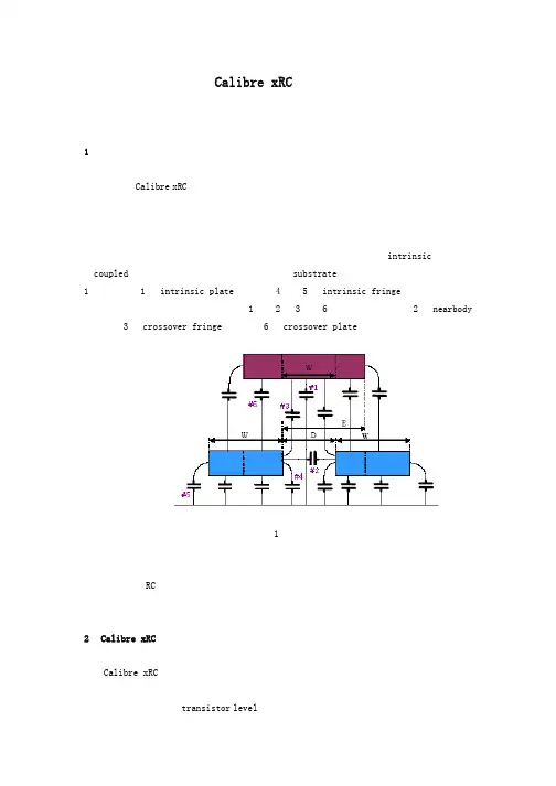
两层导电层之间会存在寄生电容,寄生电容一般可分为本征(intrinsic)和耦合(coupled)两种,本征电容是指导电层到衬底(substrate)的电容,它有两种类型,如图1中所示:#1为intrinsic plate电容,#4和#5为intrinsic fringe电容;耦合电容是指导电层在不同网线之间的电容,图1中#2、#3和#6就属于这种,其中#2为nearbody 电容,#3为crossover fringe电容,#6为crossover plate电容。
图1 寄生电容模型电路中寄生参数的存在给电路的工作造成了一定的影响,寄生电阻的存在会影响到电路的功耗,寄生RC会影响电路中的信号完整性,等等。
所以在版图完成后,必须提取出版图中的寄生参数,将它们反标入逻辑电路中一起进行仿真,以此来检查版图设计的准确性。
2.Calibre xRC功能简介Calibre xRC提供了多种寄生参数提取解决方案。
它可以根据电路设计的不同要求来提取不同的寄生参数网表,针对全定制电路和模拟电路可以提取晶体管级(transistor level)的网表,针对自动布局布线产生的电路可以提取门级(gate level)网表,针对数模混合电路可以提取混合级(ADMS)的电路网表。
它还可以根据不同的电路分析要求进行提取,针对电路的功耗(Power)分析,只进行寄生电阻的提取,针对电路的噪声(Noise)分析而仅对寄生电容的提取,针对电路的时序(Timing)分析而提取相应的RC或RCC网表,针对电路的信号完整性(Signal Integrity)分析提取寄生RC或RCC网表。
实验八寄生参数提取(PE)及信号完整性分析(SI)一、实验目的1.了解寄生参数的产生及对电路的影响。
2.掌握寄生参数提取和信号完整性分析的流程和意义。
二、实验内容1. 寄生参数提取(1)在Zeni LE窗口中,选择V erification->Layout V erification,在弹出的对话框中,选择Tool->Zeni V eri。
(2)在Command file栏里,浏览输入以下路径/zeni/v4627/demo/veri/PE_demo/pe_demo.pe,该文件是Zeni系统中PE_demo样本库所提供的用于PE提取的规则命令文件。
(3)将Custom Operation前的方框选中,选择PE选项卡。
(4)按下Appy键或OK键,Zeni开始运行PE分析。
报告结果存放在工作路径中的<cellname>.veri.log文件中。
注意:PE分析完成后,Zeni将在工作路径下生成一个以<cellname>.spi为名称的SPICE网表文件。
打开该文件可以看到,PE过程将按照提取规则,提取出版图中存在的所有器件,而不仅仅是寄生电阻和寄生电容,用户自己设计的晶体管及电容电阻等也会被一起提取出来。
该文件的名字和设计原理图时生成的网表一样,所以在PE进行时,原理图的spi网表将被覆盖。
如果需要保留,应该在PE之前将原spi网表文件换一个名字保存。
2. 局部寄生参数提取(Partial PE)(1)Partial PE执行的过程和全局PE是一样的,采用同样的PE规则命令文件。
只是在Custom Operation选项处,选择Partial PE选项卡,如下图所示。
3. 信号完整性分析(SI)在版图进行寄生参数提取(PE)之后,应该进行信号完整性分析(SI Analysis),以考察寄生参数对信号的影响程度,是否达到不可接受的程度。
目前,Zeni SI工具可以提供以下分析:Time Delay(时延分析)RC-Reduction(R,C值分析)Noise Analysis(噪声分析)(1)在PE进行完成之后,在LE窗口中,选择主菜单栏-verification,在下拉菜单中选择SI Analysis。
使用Calibre xRC实现RFCMOS电路的寄生参量提取及后仿真中国科学院微电子研究所郭慧民[摘要]Calibre xRC是Mentor Graphics公司用于寄生参量提取的工具,其强大的功能和良好的易用性使其得到业界的广泛认可。
本文以采用RFCMOS工艺实现的LNA为例,介绍使用Calibre xRC对RFCMOS电路寄生参量提取,以Calibreview 形式输出以及在Virtuoso的ADE中直接后仿真的流程。
本文还将讨论Calibre xRC特有的XCELL方式对包含RF器件的电路仿真结果的影响。
采用Calibre xRC提取寄生参量采用RFCMOS工艺设计低噪声放大器(LNA),其电路图如图1所示,版图如图2所示。
图1 LNA的电路图图2 LNA的版图Calibre支持将其快捷方式嵌入在Virtuoso平台中。
用户只需在自己.cdsinit文件中加入以下一行语句:load( strcat( getShellEnvVar("MGC_HOME") "/lib/calibre.skl" ))就可以在virtuoso的菜单中出现“calibre”一项,包含如下菜单:点击Run PEX,启动Calibre xRC的GUI,如图3所示。
Outputs菜单中的Extraction Type里,第一项通常选择Transistor Level或Gate Level,分别代表晶体管级提取和门级提取。
第二项可以选择R+C+CC,R+C,R,C+CC,其中R 代表寄生电阻,C代表本征寄生电容,CC代表耦合电容。
第三项可以选择No Inductance,L或L+M,分别代表不提取电感,只提取自感和提取自感与互感。
这些设置由电路图的规模和提取的精度而定。
在Format一栏中,可以选择SPECTRE,ELDO,HSPICE等网表形式,也可以选择Calibre xRC提供的CALIBREVIEW形式。
基于ansys Q3D仿真软件的寄生参数提取方法
在电子电路中难免存在寄生电感、寄生电容等参数,这时需要将PCB文件导出成.anf文件,再导入至ansys slave软件,现来具体描述寄生参数的提取过程
1.安装ansys electronic desktop 安装完成后会自动安装一
系列的插件
图标如图所示
2.生成.anf文件
打开PCB文件,点击file➡export➡ansoft neutral,这一步非常关键,处理不好会导致ansys 软件导入失败,注意此时文件名、路径以及PCB工程、元件参数设置均不能有中文、小数点等特殊字符出现,必须由英文、数字或下划线组成。
保存文件格式如下:
3.打开ANSYS SLAVE 软件
其界面如图所示
点击import ANF,选择刚刚保存的ANF文件打开后点击上方的export菜单中的Q3D软件
导入成功之后如下图所示
对需要仿真的net选择,然后添加source和sink,再设置analysis setup,点击对号检查,检查无误后点击叹号即可仿真。