IP5206 datasheet v1.0
- 格式:pdf
- 大小:2.40 MB
- 文档页数:11
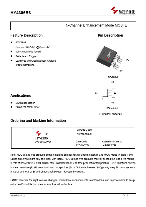
Pin1Pin7Pin1Pin2,3,5,6,7 Pin4Feature Description Pin Description●60V/290AR DS(ON)= 1.8m Ω(typ.)@V GS = 10V● 100% Avalanche Tested ● Reliable and Rugged●Lead Free and Green Devices Available (RoHS Compliant)Applications● Switch application ● Brushless Motor DriveOrdering and Marking InformationHY4306 YYXXXJWW G Note: HOOYI lead-free products contain molding compounds/die attach materials and 100% matte tin plate Termi- Nation finish;which are fully compliant with RoHS. HOOYI lead-free products meet or exceed the lead-Free require- ments of IPC/JEDEC J-STD-020 for MSL classification at lead-free peak reflow temperature. HOOYI defines “Green ” to mean lead-free (RoHS compliant) and halogen free (Br or Cl does not exceed 900ppm by weight in homogeneous material and total of Br and Cl does not exceed 1500ppm by weight).HOOYI reserves the right to make changes, corrections, enhancements, modifications, and improvements to this pr -oduct and/or to this document at any time without notice.TO-263-6LN-Channel MOSFETAbsolute Maximum RatingsNote: * Repetitive rating;pulse width limited by max.junction temperature.** Surface mounted on FR-4 board.*** Limited by T J max , starting T J=25°C, L =0.5mH, R G= 25Ω, V GS =10V. Electrical Characteristics(Tc =25°C Unless Otherwise Noted)Electrical Characteristics (Cont.) (Tc =25°C Unless Otherwise Noted)Note: *Pulse test,pulse width ≤ 300us,duty cycle ≤ 2%Typical Operating CharacteristicsFigure 1: Power Dissipation Figure 2: Drain CurrentTc-Case Temperature(℃) Tc-Case Temperature(℃)Figure 3: Safe Operation Area Figure 4: Thermal Transient ImpedanceV DS -Drain-Source Voltage(V)Maximum Effective Transient ThermalImpedance, Junction-to-CaseFigure 5: Output Characteristics Figure 6: Drain-Source On ResistanceV DS -Drain-Source Voltage (V) I D -Drain Current(A)I D -D r a i n C u r r e n t (A )I D -D r a i n C u r r e n t (A )R D S (O N )-O N -R e s i s t a n c e (Ω)Typical Operating Characteristics(Cont.)Figure 7: On-Resistance vs. Temperature Figure 8: Source-Drain Diode ForwardTj-Junction Temperature (℃)V SD -Source-Drain Voltage(V)Figure 9: Capacitance Characteristics Figure 10: Gate Charge CharacteristicsV DS -Drain-Source Voltage (V) Q G -Gate Charge (nC )C -C a p a c i t a n c e (p F )N o r m a l i z e d O n -R e s i s t a n c eI S -S o u r c e C u r r e n t (A )Avalanche Test Circuit and WaveformsSwitching Time Test Circuit and WaveformsGate Charge Test Circuit and WaveformsDevice Per UnitPackage Information TO-263-6LClassification ProfileClassification Reflow ProfilesCustomer ServiceWorldwide Sales and Service: sales@Technical Support: technical @Xi’an Hooyi Semiconductor Technology Co., Ltd.No.105,5th Fengcheng Road, Economic and Technological Development Zone, Xi'an,China TEL: (86-029) 86685706FAX: (86-029) 86685705E-mail: sales@Web net: 。
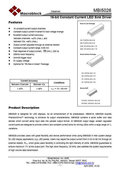
MBI5026 provides users with great flexibility and device performance while using MBI5026 in their system design for LED display applications, e.g. LED panels. Users may adjust the output current from 5 mA to 90 mA through an external resistor, R ext, which gives users flexibility in controlling the light intensity of LEDs. MBI5026 guarantees to endure maximum 17V at the output port. The high clock frequency, 25 MHz, also satisfies the system requirements of high volume data transmission.Macroblock, Inc. 2005Floor 6-4, No.18, Pu-Ting Rd., Hsinchu, Taiwan 30077, ROC.MBI5026CN\GN Outline Drawing MBI5026CNS\GNS Outline DrawingDisclaimerMacroblock reserves the right to make changes, corrections, modifications, and improvements to their products and documents or discontinue any product or service without notice. Customers are advised to consult their sales representative for the latest product information before ordering. All products are sold subject to the terms and conditions supplied at the time of order acknowledgement, including those pertaining to warranty, patent infringement, and limitation of liability.Macroblock’s products are not designed to be used as components in device intended to support or sustain life or in military applications. Use of Macroblock’s products in components intended for surgical implant into the body, or other applications in which failure of Macroblock’s products could create a situation where personal death or injury may occur, is not authorized without the express written approval of the President of Macroblock. Macroblock will not be held liable for any damages or claims resulting from the use of its products in medical and military applications.All text, images, logos and information contained on this document is the intellectual property of Macroblock. Unauthorized reproduction, duplication, extraction, use or disclosure of the above mentioned intellectual property will be deemed as infringement.。
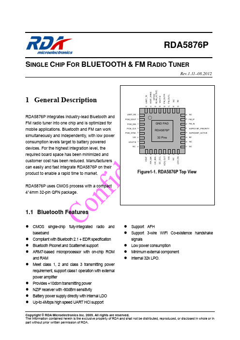
RDA5876PSINGLE CHIP FOR BLUETOOTH & FM RADIO TUNERRev.1.11–08.2012GPIO2/ WLAN_ACTIVEHOST_WAKEFM_OUTR1 General DescriptionRDA5876P integrates industry-lead Bluetooth and FM radio tuner into one chip and is optimized for mobile applications. Bluetooth and FM can work simultaneously and independently, with low power consumption levels target to battery powered devices. For the highest integration level, the required board space has been minimized and customer cost has been reduced. Manufacturers can easily and fast integrate RDA5876P on their product to enable a rapid time to market. RDA5876P uses CMOS process with a compact 4*4mm 32-pin QFN package.UART_RX 1 PCM_DOUT 2 PCM_DIN 3 PCM_CLK 4 PCM_SYNC 5 VIO 6 VOUT18 7 NC8UART_TXFM_OUTLVOUT12NC26323130292827NC2524 23NC FM_IP FM_IN AGPIO1/BT_PRIORITY AGPIO0/BT_ACTIVE RF NC NCGND PAD RDA5876P 32 Pins22 21 20 19 18 17910111213141516XIN_32KI2C_SDAXEN_OUTFigure1-1. RDA5876P Top View1.1 Bluetooth FeaturesCMOS single-chip fully-integrated radio and baseband Compliant with Bluetooth 2.1 + EDR specification Bluetooth Piconet and Scatternet support ARM7-based microprocessor with on-chip ROM and RAM Meet class 1, 2 and class 3 transmitting power requirement, support class1 operation with external power amplifier Provides +10dbm transmitting power NZIF receiver with -90dBm sensitivity Battery power supply directly with internal LDO Up-to 4Mbps high speed UART HCI supportCopyright © RDA Microelectronics Inc. 2009. All rights are reserved. The information contained herein is the exclusive property of RDA and shall not be distributed, reproduced, or disclosed in whole or in part without prior written permission of RDA.Support AFH Support 3-wire WIFI Co-existence handshake signals Low power consumption Minimum external component Internal 32k LPO.LDO_ONI2C_SCLVBATXINNCRDA Microelectronics, Inc.RDA5876P Datasheet V1.111.2 FM FeaturesCMOS single-chip fully-integrated FM tuner Low power consumption Total current consumption lower than 20mA at 3.0V power supply Support worldwide frequency band 50 -115 MHz Support flexible channel spacing mode 100KHz, 200KHz, 50KHz and 25KHz Support RDS/RBDS Digital low-IF tuner Image-reject down-converter High performance A/D converter IF selectivity performed internally Fully integrated digital frequency synthesizer Fully integrated on-chip RF and IF VCO Fully integrated on-chip loop filter Autonomous search tuning Support 32.768KHz crystal oscillator Digital auto gain control (AGC) Digital adaptive noise cancellation Mono/stereo switch Soft mute High cutProgrammable de-emphasis (50/75 μs) Receive signal strength indicator (RSSI) Bass boost Volume control Line-level analog output voltage I2C control bus interface Directly support 32Ω resistance loading Integrated LDO regulator 1.8 to 5.5 V operation voltage1.3 ApplicationsMobile handset MP3,MP4 and PMP PDA Cordless phoneThe information contained herein is the exclusive property of RDA and shall not be distributed, reproduced, or disclosed in whole or in part without prior written permission of RDA. Page 2 of 22RDA Microelectronics, Inc.RDA5876P Datasheet V1.112 Table of Contents1 General Description ....................................................................................................................................1 1.1 Bluetooth Features .............................................................................................................................1 1.2 FM Features........................................................................................................................................2 1.3 Applications ........................................................................................................................................2 Table of Contents.........................................................................................................................................3 Bluetooth Section Functional Description.................................................................................................4 Bluetooth Section Features.........................................................................................................................5 Bluetooth Section Electrical Characteristics ............................................................................................6 Bluetooth Section Radio Characteristics...................................................................................................8 FM Section Functional Description .........................................................................................................10 FM Section Electrical Characteristics.....................................................................................................12 FM Section Receiver Characteristics ......................................................................................................13 Pins Description.........................................................................................................................................14 Application Circuit....................................................................................................................................17 Package Physical Dimension ....................................................................................................................17 PCB Land Pattern.....................................................................................................................................18 Change List................................................................................................................................................21 Contact Information .................................................................................................................................222 3 4 5 6 7 8 9 10 11 12 13 14 15The information contained herein is the exclusive property of RDA and shall not be distributed, reproduced, or disclosed in whole or in part without prior written permission of RDA. Page 3 of 22RDA Microelectronics, Inc.RDA5876P Datasheet V1.113 Bluetooth Section Functional DescriptionVBATDC/DCBBModemA AΦ BT_RF PLLx xRFLDOROMROMDEnvelonFM_IP LDO_ONPORRAMRAMFM_IN GPIO_FM1AHB ARM TRAP SPI2 FMGPIO_FM2 GPIO_FM3 FM_OUTRVICI2C_SDA I2C_SCLSCUFM_OUTLI2C DMA TIMER PLLXINUART_TX UART_RXUARTAPB BRIDGEAPB GPIO 32K/LPOXIN_32KFigure3-1. RDA5876P Bluetooth Block Diagram RDA5876P is designed for use in UART HCI with handset chipsets. As shown in Figure3-1, RDA5876P integrates radio unit, baseband core, ARM7 core and memory which provides a complete lower Bluetooth protocol stack including the LC, LM and HCI interface.The information contained herein is the exclusive property of RDA and shall not be distributed, reproduced, or disclosed in whole or in part without prior written permission of RDA. Page 4 of 22RDA Microelectronics, Inc.RDA5876P Datasheet V1.114 Bluetooth Section FeaturesRadio♦ ♦ ♦ ♦ ♦ ♦ ♦ Build-in TX/RX switch Fully integrated synthesizer without any external component Support external reference clock direct input Class1, 2 and class3 transmit output power supported and over 30dB dynamic control range Supports π/4 DQPSK and 8DPSK modulation High performance in receiver sensitivity and over 80dB dynamic range Integrated channel filterAuxiliary features♦ ♦ ♦ ♦ ♦ On-chip regulator to support battery power supply directly Power management support low power mode Support share handset system reference clock Support 3-wire wifi cooperation handshake protocol Support external class1 PA and antenna switchBaseband♦ ♦ ♦ ♦ ♦ Internal RAM allows fully speed data transfer, mixed voice and data, and fully piconet operation Logic for forward error correction, header error control, access code correlation, CRC, demodulation , encryption bit stream generation, whitening and transmit pulse shaping Support eSCO and AFH Support up to Bluetooth v2.1 + EDR Support A-law, μ-law and CVSD digitize audio CODEC in PCM interfaceInterface♦ ♦ ♦ ♦ Provides UART HCI interface, up-to 4Mbps Provides I2C interface for host to do configuration Provides PCM audio interface Provides 3-wire and 2-wire WIFI Co-existence handshake interfaceBluetooth Stack♦ Compliant with Bluetooth 2.1 + EDR specificationThe information contained herein is the exclusive property of RDA and shall not be distributed, reproduced, or disclosed in whole or in part without prior written permission of RDA. Page 5 of 22RDA Microelectronics, Inc.RDA5876P Datasheet V1.115 Bluetooth Section Electrical CharacteristicsTable 5-1SYMBOLDC Electrical Specification (Recommended Operation Conditions):DESCRIPTION Supply Voltage from battery or LDO Ambient Temperature CMOS Low Level Input Voltage CMOS High Level Input Voltage CMOS Threshold Voltage MIN 3.3 -20 0 0.7*VIO 0.5*VIO TYP 4.0 27 MAX 4.2 +50 0.3*VIO VIO UNIT V ℃ V V VVBAT Tamb VIL VIH VTHNotes:1. VIO=1.8~3.3VTable 5-2SYMBOLDC Electrical Specification (Absolute Maximum Ratings):DESCRIPTION Ambient Temperature Input Current Input Voltage LNA Input Level MIN -20 -10 -0.3 TYP MAX +60 +10 VIO+0.3 +5 UNIT °C mA V dBmTamb IIN VIN VlnaTable 5-3LDOPower consumption specification(VBAT = 4.0 V, VIO = 2.8V, TA = +27℃, RF 9dBm, LDO mode unless otherwise specified) STATE Headset voice Headset SNIFF HCI only active Both SCAN DeepSleep internal LDO off 1.28S cycle 26Mhz crystal off LDO_ON off INQUIRE and PAGE SCAN DESCRIPTION HV3 type 500ms cycle NO INQUIRE and PAGE SCAN Condition TYP 18 0.5 5.7 1.0 118 7 UNIT mA mA mA mA μA μAIvbat=105uA,Ivio=13uA,External 32K input Ivbat=6uA,Ivio=1uAThe information contained herein is the exclusive property of RDA and shall not be distributed, reproduced, or disclosed in whole or in part without prior written permission of RDA. Page 6 of 22RDA Microelectronics, Inc.RDA5876P Datasheet V1.116 Bluetooth Section Radio CharacteristicsTable 6-1 Receiver Characteristics ------ Basic Data Rate(VBAT = 4.0 V, TA = 27°C, unless otherwise specified) SYMBOL PARAMETER CONDITIONS MIN / 0 / F=F0 + 1MHz F=F0 - 1MHz Adjacent channel selectivity C/I F=F0 + 2MHz F=F0 - 2MHz F=F0 + 3 MHz F=F0 - 3MHz Adjacent channel selectivity C/I F=Fimage 30MHz–2000MHz Out-of-band blocking performance 2000MHz–2400MHz 2500MHz–3000MHz 3000MHz–12.5GHz Intermodulation Spurious output level / / / / / / / -10 -27 -27 -10 -35 -150 TYP -90 / +10 / / / / / / / / / / / / / MAX / / / -5 0 -33 -30 -45 -40 0 / / / / / / UNIT dBm dBm dB dB dB dB dB dB dB dB dBm dBm dBm dBm dBm dBm/HzGeneral specificationsSensitivity @0.1% BER Maximum received signal@0.1% BER C/I c-channelNotes:Table 6-2Transmit Characteristics ------ Basic Data Rate(VBAT = 4.0V, TA = 27 °C, unless otherwise specified) SYMBOL General specifications PARAMETER CONDITIONS MIN / 20 / F=F0 + 1MHz F=F0 - 1MHz F=F0 + 2MHz F=F0 - 2MHz F=F0 + 3MHz F=F0 - 3MHz F=F0 + >3MHz / / / / / / / TYP +4 / 0.9 -20 -20 -35 -35 -40 -40 / MAX +10 / / / / / / / / -46 UNIT dBm dB MHz dBm dBm dBm dBm dBm dBm dBmMaximum RF transmit power RF power control range 20dB band widthAdjacent channel transmit powerThe information contained herein is the exclusive property of RDA and shall not be distributed, reproduced, or disclosed in whole or in part without prior written permission of RDA. Page 7 of 22RDA Microelectronics, Inc.F=F0 - >3MHz △f1avg Maximum modulation △f2max Minimum modulation △f2avg/△f1avg ICFT Drift rate Drift (1 slot packet) Drift (5 slot packet) -46 / / 0.80 / / / /RDA5876P Datasheet V1.11 / 164 145 / +4 0.1 -2 -2 / / / / / / / / dBm kHz kHz / kHzkHz/50uskHz kHzNotes:Table 6-3Receiver Characteristics ------ Enhanced Data Rate(VBAT = 4.0 V, TA = 27°C, unless otherwise specified) PARAMETER CONDITIONS MIN / 0 / F=F0 + 1MHz F=F0 - 1MHz Adjacent channel selectivity C/I F=F0 + 2MHz F=F0 - 2MHz F=F0 + 3MHz F=F0 - 3MHz Adjacent channel selectivity C/I F=Fimage / / / / / / / TYP -86 / / / / / / / / / MAX / / +13 +5 0 -20 -20 -40 -40 -7 UNIT dBm dBm dB dB dB dB dB dB dB dBπ/4 DQPSK Sensitivity @0.01% BER Maximum received signal@0.1% BER C/I c-channel8DPSKSensitivity @0.01% BER Maximum received signal@0.1% BER C/I c-channelF=F0 + 1MHz F=F0 - 1MHz Adjacent channel selectivity C/I F=F0 + 2MHz F=F0 - 2MHz F=F0 + 3MHz F=F0 - 3MHz Adjacent channel selectivity C/I F=Fimage/ 0 / / / / / / / /-83 / / / / / / / / // / +18 +5 +5 -20 -20 -35 -35 0dBm dBm dB dB dB dB dB dB dB dBNotes:The information contained herein is the exclusive property of RDA and shall not be distributed, reproduced, or disclosed in whole or in part without prior written permission of RDA. Page 8 of 22RDA Microelectronics, Inc.RDA5876P Datasheet V1.11Table 6-4Transmit Characteristics ------ Enhanced Data Rate(VBAT = 4.0 V, TA = 27°C, unless otherwise specified) PARAMETER General specifications CONDITIONS MIN / / / / / / / / RMS DEVM / / / / / / / / / / / / / / 99% DEVM Peak DEVM RMS DEVM TYP +2 -1.6 +7.4 +6.7 +2.4 +7.1 +4.4 +2.7 4.7 / 8.8 4.6 / 11.3 -14.7 -15.2 -51.0 -51.2 -30 -30 / 100 MAX / / / / / / / / / 30 / / 20 / / / / / / / -32 / UNIT dBm dB kHz kHz kHz kHz kHz kHz kHz % % % % % % dBm dBm dBm dBm dBm dBm dBm %Maximum RF transmit powerRelative transmit controlπ/4 DQPSK max w0 π/4 DQPSK max wi π/4 DQPSK max |wi + w0| 8DPSK max w0 8DPSK max wi 8DPSK max |wi + w0| π/4 DQPSK Modulation Accuracy8DPSK Modulation Accuracy99% DEVM Peak DEVM F=F0 + 1MHz F=F0 - 1MHz F=F0 + 2MHzIn-band spurious emissionsF=F0 - 2MHz F=F0 + 3MHz F=F0 - 3MHz F=F0 +/- > 3MHzEDR Differential Phase CodingNotes:The information contained herein is the exclusive property of RDA and shall not be distributed, reproduced, or disclosed in whole or in part without prior written permission of RDA. Page 9 of 22RDA Microelectronics, Inc.RDA5876P Datasheet V1.117 FM Section Functional DescriptionLOUTI PGALNAP LNAN LNA +I ADCAudio DSP Coredigital filter MPX decoder stereo/mono audioL DACLimiterQ PGAQ ADCR DACROUT32.768 KHzVCO SynthesizerRDS /RBDS RSSIGPIOGPIORCLK 2.7-5.5 V VDDSCLKMCU LDOInterface Bus SDIO VIOFM ReceiverFigure 7-1. RDA5876P FM Tuner Block Diagram The PGA amplifies the mixer output IF signal and then digitized with ADCs. The DSP core finishes the channel selection, FM demodulation, stereo MPX decoder and output audio signal. The MPX decoder can autonomous switch from stereo to mono to limit the output noise. The DACs convert digital audio signal to analog and change the volume at same time. The DACs has low-pass feature and -3dB frequency is about 30 KHz. Synthesizer The frequency synthesizer generates the local oscillator signal which divide to quadrature, then be used to downconvert the RF input to a constant low intermediate frequency (IF). The synthesizer reference clock is 32.768 KHz. The synthesizer frequency is defined by bits CHAN[9:0] with the range from 50MHz to 115MHz.The receiver uses a digital low-IF architecture that avoids the difficulties associated with direct conversion while delivering lower solution cost and reduces complexity, and integrates a low noise amplifier (LNA) supporting the FM broadcast band (50 to 115MHz), a quadrature image-reject mixer, a programmable gain control (PGA), a high resolution analog-to-digital converters (ADCs), an audio DSP and a highfidelity digital-to-analog converters (DACs). The LNA has differential input ports (LNAP and LNAN) and supports any input port by set according registers bits (LNA_port_sel[1:0]). It default input common mode voltage is GND. The limiter prevents overloading and limits the amount of intermodulation products created by strong adjacent channels. The quadrature mixer down converts the LNA output differential RF signal to low-IF, it also has image-reject function.The information contained herein is the exclusive property of RDA and shall not be distributed, reproduced, or disclosed in whole or in part without prior written permission of RDA. Page 10 of 22RDA Microelectronics, Inc. Power Supply The RDA5876P FM section integrated LDO which supplies power to the chip. The external supply voltage range is 1.8-5.5 V. RESET and Control Interface select The RDA5876P FM section is RESET itself When VIO is Power up. And also support soft reset by trigger 02H BIT1 from 0 to 1. The control interface is I2C. Control Interface The I2C interface is compliant to I2C Bus Specification 2.1. It includes two pins: SCL and SDA. A I2C interface transfer begins with START condition, a command byte and data bytes, each byte has a followed ACK (or NACK) bit, and ends with STOP condition. The command byte includes a 7-bit chip address (0010000b) and a R/W bit. The ACK (or NACK) is always sent out by receiver. When in write transfer, data bytes is written out from MCU, and when in read transfer, data bytes is read out from RDA5876P. There is no visible register address in I2C interface transfers. The I2C interface has a fixed start register address (0x02h for write transfer and 0x0Ah for read transfer), and an internal incremental address counter. If register address meets the end of register file, 0x3Ah, register address will wrap back to 0x00h. For write transfer, MCU programs registers from register 0x02h high byte, then register 0x02h low byte, then register 0x03h high byte, till the last register. RDA5876P always gives out ACK after every byte, and MCU gives out STOP condition when register programming is finished. For read transfer, after command byte from MCU, RDA5876P sends out register 0x0Ah high byte, then register 0x0Ah low byte, then register 0x0Bh high byte, till receives NACK from MCU. MCU gives out ACK for data bytes besides last data byte. MCU gives out NACK for last data byte, and then RDA5876P will return the bus to MCU, and MCU will give out STOP condition. Details please refer to RDA5876P Programming Guide and RDA5802N Programming Guide and Datasheet.RDA5876P Datasheet V1.11The information contained herein is the exclusive property of RDA and shall not be distributed, reproduced, or disclosed in whole or in part without prior written permission of RDA. Page 11 of 22RDA Microelectronics, Inc.RDA5876P Datasheet V1.118 FM Section Electrical CharacteristicsTable 8-1 DC Electrical Specification (Recommended Operation Conditions): SYMBOL VBAT VIO Tamb VIL VIH VTHNotes: 1. VIO=1.8~3.3VDESCRIPTION Supply Voltage Interface Supply Voltage Ambient Temperature CMOS Low Level Input Voltage CMOS High Level Input Voltage CMOS Threshold VoltageMIN 3.3 1.5 -20 0 0.7*VIOTYP 4.0 3.0 27MAX 4.2 3.6 +75 0.3*VIO VIOUNIT V V ℃ V V V0.5*VIOTable 8-2 DC Electrical Specification (Absolute Maximum Ratings): SYMBOL VIO Tamb IIN VIN Vlna Notes: 1. For Pin: SCL, SDA DESCRIPTION Interface Supply Voltage Ambient Temperature Input Current (1) Input Voltage(1) LNA FM Input Level MIN -0.5 -40 -10 -0.3 TYP MAX +3.6 +90 +10 VIO+0.3 +10 UNIT V °C mA V dBmTable 8-3 Power Consumption Specification (VBAT = 4.0 V, VIO=1.5 to 3.6V, TA = -25 to 85 ℃, unless otherwise specified) SYMBOL IA IVIO IAPD IVIO DESCRIPTION Analog Supply Current Interface Supply Current Analog Powerdown Current Interface Powerdown Current Condition ENABLE=1 SCL and SDA inactive ENABLE=0 ENABLE=0 TYP 20 90 5 10 UNIT mA μA μA μAThe information contained herein is the exclusive property of RDA and shall not be distributed, reproduced, or disclosed in whole or in part without prior written permission of RDA. Page 12 of 22RDA Microelectronics, Inc.RDA5876P Datasheet V1.119 FM Section Receiver CharacteristicsTable 9-1 Receiver Characteristics (VBAT = 4.0 V, VIO= 3.0V, TA = 25 °C, unless otherwise specified)SYMBOL PARAMETER FM Input Frequency Range CONDITIONS Adjust BAND Register 50MHz 65MHz 88MHz 98MHz 108MHz 115MHz MIN 50 80 60 50 60 55 53 35 Single-ended Volume[3:0] =1111 Rload=1KΩ Rload=32Ω 32 Volume[3:0]=0000 1KHz=0dB ±3dB point Low Freq9TYPMAX 115UNIT MHzGeneral specificationsFin1.4 1.2 1.2 1.3 1.3 1.3 70 85 360 57 55 0.15 0.2 100 141.8 1.5 1.5 1.5 1.5 1.8 0.2 0.05 dBμV dB dB dB mV dB dB Ω % dB dB Hz μV EMFVrfSensitivity1,2,3S/N=26dBIP3inInput IP34AGCD=11,2αamS200 S400 VAFL; VAFR S/NAM Suppressionm=0.3 ±200KHz ±400KHz1,2Adjacent Channel Selectivity 400KHz Selectivity Audio L/R Output Voltage (Pins LOUT and ROUT) Maximum Signal to Noise Ratio1,2,3,5Volume [3:0] =1111 Mono2 Stereo6αSCS RLTHDStereo Channel Separation Audio Output Loading Resistance Audio Total Harmonic Distortion1,3,6αAOIRmute BWaudioAudio Output L/R Imbalance1,6 Mute Attenuation Ratio1 Audio Response160 -High FreqPins LNAN, LNAP, LOUT, ROUT and NC(22,23)Vcom_rfin Vcom Vcom_ncPinsLNAN/LNAPInputCommon Mode Voltage Audio Output Common Mode Voltage8 Pins NC ( 22,23 ) Common Mode Voltage 1.00 1.05 1.1V V VFloatingNotes:1. Fin=65 to 115MHz; Fmod=1KHz; de-emphasis=75μs; MONO=1; L=R unless noted otherwise;2. Δf=22.5KHz; 3. BAF = 300Hz to 15KHz, RBW <=10Hz; 6. Δf=75KHz,fpilot=10% 5. PRF=60dBUV; 8. At LOUT and ROUT pins 4. |f2-f1|>1MHz, f0=2xf1-f2, AGC disable, Fin=76 to 108MHz; 7. Measured at VEMF = 1 m V, f RF = 65 to 108MHz 9. AdjustableThe information contained herein is the exclusive property of RDA and shall not be distributed, reproduced, or disclosed in whole or in part without prior written permission of RDA. Page 13 of 22RDA Microelectronics, Inc.RDA5876P Datasheet V1.1110 Pins DescriptionGPIO2/ WLAN_ACTIVE HOST_WAKEFM_OUTRUART_TXFM_OUTLVOUT12323130292827NC26UART_RX 1 PCM_DOUT 2 PCM_DIN 3 PCM_CLK 4 PCM_SYNC 5 VIO 6 VOUT18 7 NC 8NC2524 23NC FM_IP FM_IN AGPIO1/BT_PRIORITY AGPIO0/BT_ACTIVE RF NC NCGND PAD RDA5876P 32 Pins22 21 20 19 18 17910111213141516XIN_32KI2C_SDAXEN_OUTFigure10-1. RDA5876P Top ViewThe information contained herein is the exclusive property of RDA and shall not be distributed, reproduced, or disclosed in whole or in part without prior written permission of RDA. Page 14 of 22LDO_ONI2C_SCLVBATXINNCRDA Microelectronics, Inc.RDA5876P Datasheet V1.11Table 10-1RDA5876P Pins DescriptionPINNO.DESCRIPTIONUART_RX PCM_DOUT PCM_DIN PCM_CLK PCM_SYNC VIO VOUT18 NC VBAT XIN_32K I2C_SDA I2C_SCL XEN_OUT XIN NC LDO_ON NC NC RF AGPIO0 AGPIO1 FM_IN FM_IP NC NC NC FM_OUTL FM_OUTR VOUT12 GPIO2 HOST_WAKE UART_TX1 2 3 4 5 6 7 8 9 10 11 12 13 14 15 16 17 18 19 20 21 22 23 24 25 26 27 28 29 30 31 32UART data input Synchronous data output Synchronous data input Synchronous data clock Synchronous data sync IO power supply Analog voltage output, connected with decouple capacitor Should be not connected Bluetooth and FM power supply 32.768K clock input I2C interface Data signal I2C interface Clock signal Clock request output For 26Mhz external clock input Should be not connected Internal LDO power on Should be not connected Should be not connected Bluetooth Radio signal Programmable I/O Also used ad bt_active when using WIFI co-existence handshake interface. Programmable I/O. Also used as bt_priority when using WIFI co-existence handshake interface. LNA input port. For single-ended input, LNAN should be connected to RFGND LNA input port. For single-ended input, LNAN should be connected to RFGND Should be not connected Should be not connected Should be not connected Left audio output Right audio output Digital voltage output, connected with decouple capacitor Programmable I/O. Also used as wl_active when using WIFI co-existence handshake interface. Output to wakeup host UART data outputThe information contained herein is the exclusive property of RDA and shall not be distributed, reproduced, or disclosed in whole or in part without prior written permission of RDA. Page 15 of 22RDA Microelectronics, Inc.RDA5876P Datasheet V1.1111 Application CircuitThe information contained herein is the exclusive property of RDA and shall not be distributed, reproduced, or disclosed in whole or in part without prior written permission of RDA. Page 16 of 22RDA Microelectronics, Inc.RDA5876P Datasheet V1.1112 Package Physical DimensionFigure12-1illustratesthepackage RoHS-compliant. details for the RDA5876P. The package is lead-free andThe information contained herein is the exclusive property of RDA and shall not be distributed, reproduced, or disclosed in whole or in part without prior written permission of RDA. Page 17 of 22RDA Microelectronics, Inc. Figure12-1. 32-Pin 4x4 Quad Flat No-Lead (QFN)RDA5876P Datasheet V1.1113 PCB Land PatternFigure13-3.Classification Reflow ProfileTable 13-1Classification Reflow ProfilesSn-Pb Eutectic Assembly 3 ℃/second max. Pb-Free Assembly 3 ℃/second max.Profile Feature Average Ramp-Up Rate (TSmax to Tp) Preheat -Temperature Min (Tsmin) -Temperature Max (Tsmax) -Time (tsmin to tsmax) Time maintained above: -Temperature (TL) -Time (tL) Peak /Classification Temperature(Tp) Time within 5 oC of actual Peak Temperature (tp) Ramp-Down Rate Time 25 oC to Peak100 ℃ 100 ℃ 60-120 seconds 183 ℃ 60-150seconds See Table 9-2 10-30 seconds 6 ℃/second max. 6 minutes max.150 ℃ 200 ℃ 60-180 seconds 217℃ 60-150 seconds See Table 9-3 20-40 seconds 6 ℃/seconds max. 8 minutes max.The information contained herein is the exclusive property of RDA and shall not be distributed, reproduced, or disclosed in whole or in part without prior written permission of RDA. Page 18 of 22RDA Microelectronics, Inc. TemperatureRDA5876P Datasheet V1.11Table 13-2 Pb-free Process – Package Peak Reflow Temperatures Package Thickness Volume mm3 <350<2.5mm ≥2.5mm 240 + 0/-5 ℃ 225 + 0/-5 ℃Volume mm3 ≥350 225 + 0/-5 ℃ 225 + 0/-5 ℃Table 13-3 Pb-free Process – Package Classification Reflow Temperatures Package Volume mm3 Volume mm3 Volume mm3 Thickness 350-2000 <350 >2000<1.6mm 1.6mm – 2.5mm ≥2.5mm 260 + 0 ℃ * 260 + 0 ℃ * 250 + 0 ℃ * 260 + 0 ℃ * 250 + 0 ℃ * 245 + 0 ℃ * 260 + 0 ℃ * 245 + 0 ℃ * 245 + 0 ℃ **Tolerance : The device manufacturer/supplier shall assure process compatibility up to and including the stated classification temperature(this mean Peak reflow temperature + 0 ℃. For example 260+ 0 ℃ ) at the rated MSL Level. Note 1: All temperature refer topside of the package. Measured on the package body surface. Note 2: The profiling tolerance is + 0 ℃, - X ℃ (based on machine variation capability)whatever is required to control the profile process but at no time will it exceed – 5 ℃. The producer assures process compatibility at the peak reflow profile temperatures defined in Table 13-3. Note 3: Package volume excludes external terminals(balls, bumps, lands, leads) and/or non integral heat sinks. Note 4: The maximum component temperature reached during reflow depends on package the thickness and volume. The use of convection reflow processes reduces the thermal gradients between packages. However, thermal gradients due to differences in thermal mass of SMD package may sill exist. Note 5: Components intended for use in a “lead-free” assembly process shall be evaluated using the “lead free” classification temperatures and profiles defined in Table13-1, 13-2, 13-3 whether or not lead free.RoHS CompliantThe product does not contain lead, mercury, cadmium, hexavalent chromium, polybrominated biphenyls (PBB) or polybrominated biphenyl ethers (PBDE), and are therefore considered RoHS compliant.ESD SensitivityIntegrated circuits are ESD sensitive and can be damaged by static electricity. Proper ESD techniques should be used when handling these devices.The information contained herein is the exclusive property of RDA and shall not be distributed, reproduced, or disclosed in whole or in part without prior written permission of RDA. Page 19 of 22。
ORIGINATE DATEEDIT DATE PAGE 1545 Barber Lane, Milpitas, CA 95035 U.S.A.PI5USB30216CXUA Demo Board Rev.B User ManualMeasurement by: NA Report by: Lee, JustinTable of Contents1 Introduction ..................................................................................................................................2 2 Overview ....................................................................................................................................... 23 Quick Start ....................................................................................................................................4 3.1 Source(DFP) Mode ................................................................................................................... 4 3.2 Battery-powered Sink(UFP) Mode ...........................................................................................5 3.3 Bus-powered Sink(UFP) Mode ................................................................................................6 3.4 Try.SNK DRP Mode ..................................................................................................................7 4 Circuit Description ....................................................................................................................... 9 4.1 DIP Switch Setting .................................................................................................................... 9 4.2 Mode Selection, I2C Address and I2C Bus ............................................................................ 9 4.3 VBUS Power Supply ................................................................................................................. 9 4.4 Power ...................................................................................................................................... 10 4.5 Disable/Low Power State ....................................................................................................... 10 5 Appendix A: Demo Board Schematic....................................................................................... 12 6Appendix B: Demo Board Picture (13)ORIGINATE DATEEDIT DATE PAGE 1545 Barber Lane, Milpitas, CA 95035 U.S.A.1 IntroductionPI5USB30216C provides a cost-effective solution for USB 2.0 Type-C connector applications. PI5USB30216C detects the plug-in orientation of the cable at a Type-C connector. It supports host mode, device mode and dual role mode ports with automatic configuration based on the voltage levels detected on CC pins. It is a fully-integrated solution with ultra-low power dissipation. PI5USB30216C enters power-saving mode when ENB pin is pulled up to VDD through an internal resistor.PI5USB30216C supports both pin and I2C control base on ADDR pin setting. It allows the system choose between pin control and I2C control mode. In pin control mode, the PORT input pin determines the port setting in which host, device or dual-role port can be selected. In host mode, the system can monitor ID pin to know the connector status while default current mode is set. Systems running in device mode can monitor system VBUS for connector status as well as OUT1 and OUT2 pins for host’s charging profile capability. Enabling I2C control mode allows higher flexibility for port control and communications through registers read/write in PI5USB30216C. There is also flexibility to support Default, 1.5A and 3A current modes. An interrupt signal for indicating changes with the I2C registers is sent to the master to notify the system any change in the Type-C connector while in parallel the system can still monitor ID pin.This user manual describes the components and the usage of PI5USB30216C Demo Board Rev.B.2 OverviewFigure 1 is the block diagram of Diodes PI5USB30216C demo board and figure 2 shows the demo board layout. A USB-C cable can be connected between the USB-C receptacle connector (J1) on PI5USB30216C demo board and another USB-C device. A USB-C to USB-A cable can be connected between J1 and a USB host, such as PC. A USB-C to USB-A receptacle adapter can be connected between J1 and a USB device, such as USB flash drive. One USB3 micro-AB receptacle (J2) is used to connect mobile phones/notebook/tablet/PC to transmit USB2 data to/from J1.Slide switch at reference SW1 is used to set control mode (GPIO/I2C) and operating mode (Source/Sink/DRP) of PI5USB30216C and LED indicator to SDA/SCL/INTB/ID pins of PI5USB30216C. The processor can connect to SDA/SCL/INTB/ID pins through Test Header J3.+5V can be employed to the demo board via 5VPW header pin or mini-B receptacle (J4).VBUS of Type-C connector can be source from on-board VBUS switch via JP1.ORIGINATE DATEEDIT DATE PAGE 1545 Barber Lane, Milpitas, CA 95035 U.S.A.Figure 1: Simplified Block Diagram of PI5USB30216C Demo Board Rev.BFigure 2: Layout of PI5USB30216C Demo Board Rev.BORIGINATE DATEEDIT DATE PAGE 1545 Barber Lane, Milpitas, CA 95035 U.S.A.3 Quick StartThis section provides different configuration examples to start-up PI5USB30216C demo board rev.B in Source, Sink or DRP mode. 3.1 Source (DFP) ModeTo start-up the PI5USB30216C demo board rev.B in pin control DFP mode, complete the following steps: 1. Configure pin headers and DIP switches SW1 as shown in Table 1.2. Power-up PI5USB30216C demo board by connecting J2 to a USB host using Type-A to micro-B cable. D2 should lightup indicating the board has power.3. Connect PI5USB30216C demo board to a Type-C Sink(UFP) using a Type-C cable. D6 should light up indicating IDpin is pulled low and 5V VBUS is provided by the demo board. .Figure 3: PI5USB30216C Demo Board DFP mode illustration.Header pin/Switch Pin name/ Function Setting SW1.1 ENB = LON SW1.2 SCL/OUT2 LED indicator OFF SW1.3 SDA/OUT1 LED indicatorOFF SW1.4 ADDROFF SW1.5 INTB/OUT3 LED indicatorON SW1.6 ID LED indicator ON SW1.7 PORT = H ON SW1.8 PORT = LOFF JP1 Connect output of VBUS switch to VBUSCON JP3 Demo board power by VBUSA ON JP5 Connect VBUSC to VBUSA OFF JP9 Connect 5VPW to VDD OFF JP10Enable 3.3V VDDONTable 1: PI5USB30216C Demo Board Rev.B DFP mode configuration.ORIGINATE DATEEDIT DATE PAGE 1545 Barber Lane, Milpitas, CA 95035 U.S.A.3.2 Battery-powered Sink (UFP) ModeTo start-up the PI5USB30216C demo board rev.B in pin control UFP mode, complete the following steps: 1. Configure pin headers and DIP switches SW1 as shown in Table 2. 2. Connect J2 to a USB device using micro-A to Type-A receptacle.3. Power up PI5UB30216C demo board by connecting J4 to a USB host using Type-A to mini-B cable (or connect +5V to5VPW pin header). D2 should light up indicating the board has power.4. Connect PI5USB30216C demo board to a Type-C Source(DFP) using a Type-C cable. 5V VBUS should be providedby the Type-C Host/Source/DFP. D3 and D4 might light up depends on the DFP’s Type-C current mode setting.Figure 4: PI5USB30216C Demo Board battery-powered UFP mode illustration.Header pin/Switch Pin name/ Function Setting SW1.1 ENB = LON SW1.2 SCL/OUT2 LED indicator ON SW1.3 SDA/OUT1 LED indicatorON SW1.4 ADDROFF SW1.5 INTB/OUT3 LED indicatorOFF SW1.6 ID LED indicator OFF SW1.7 PORT = H OFF SW1.8 PORT = LON JP1 Enable On-board VBUS switch OFF JP3 Demo board power by VBUSA OFF JP5 Connect VBUSC to VBUSA ON JP9 Connect 5VPW to VDD OFF JP10 Enable 3.3V VDDONTable 2: PI5USB30216C Demo Board Rev.B battery-powered UFP mode configuration.ORIGINATE DATEEDIT DATE PAGE 1545 Barber Lane, Milpitas, CA 95035 U.S.A.3.3 Bus-powered Sink(UFP) ModeTo start-up the PI5USB30216C demo board rev.B in pin control VBUS-powered UFP mode, complete the following steps: 1. Configure pin headers and DIP switches SW1 as shown in Table 3. 2. Connect J2 to a USB device using micro-A to Type-A receptacle.3. Connect PI5USB30216C demo board to a Type-C Source(DFP) using a Type-C cable. 5V VBUS should be providedby the Type-C Host/Source/DFP. D2, D3 and D4 might light up depends on the DFP’s Type-C current mode setting.Figure 5: PI5USB30216C Demo Board VBUS-powered UFP mode illustration.Header pin/ Switch Pin name/ Function Setting SW1.1 ENB = LON SW1.2 SCL/OUT2 LED indicator ON SW1.3 SDA/OUT1 LED indicatorON SW1.4 ADDROFF SW1.5 INTB/OUT3 LED indicatorOFF SW1.6 ID LED indicator OFF SW1.7 PORT = H OFF SW1.8 PORT = LON JP1 Enable On-board VBUS switch OFF JP3 Demo board power by VBUSA ON JP5 Connect VBUSC to VBUSA ON JP9 Connect 5VPW to VDD OFF JP10 Enable 3.3V VDDONTable 3: PI5USB30216C Demo Board Rev.B VBUS-powered UFP mode configuration.ORIGINATE DATEEDIT DATE PAGE 1545 Barber Lane, Milpitas, CA 95035 U.S.A.3.4 Try.SNK DRP ModeTo start-up the PI5USB30216C demo board rev.B in pin control Try.SNK DRP mode, complete the following steps: 1. Configure pin headers and DIP switches SW1 as shown in Table 3 in the next page.2. Power up PI5UB30216C demo board by connecting J4 to a USB host using Type-A to mini-B cable. D2 should light upindicating the board has power.3. Connect PI5USB30216C demo board to a Type-C Sink(UFP) using a Type-C cable. D6 should light up indicating IDpin is pulled low and 5V VBUS is provided by the demo board.4. Connect PI5USB30216C demo board to a Type-C Source(DFP) using a Type-C cable. 5V VBUS should be providedby the Type-C Host/Source/DFP. D3 and D4 might light up depends on the DFP’s Type-C current mode setting5. Connect PI5USB30216C demo board to a Type-C DRP using a Type-C cable. PI5USB30216C should connect asSink/UFP due to Try.SNK feature. 5V VBUS should be provided by the port partner. D3 and D4 might light up depends on port partner’s Type-C current mode setting.6. Connect PI5USB30216C demo board to a Type-C Try.SNK DRP using a Type-C cable. PI5USB30216C may result ineither DFP or UFP mode. The result is random.a. When connect as a Source/DFP/Host, D6 should light up indicating ID pin is pulled low and 5V VBUS is providedby the demo board.b. When connect as a Sink/UFP/Device. 5V VBUS should be provided by the port partner. D3 and D4 might light updepends on port partner’s Type-C current mode setting.Figure 6: PI5USB30216C Demo Board Try.SNK DRP mode illustration.ORIGINATE DATE EDIT DATE PAGE 1545 Barber Lane, Milpitas, CA 95035 U.S.A.Header pin/ Switch Pin name/ Function Setting SW1.1 ENB = LON SW1.2 SCL/OUT2 LED indicator ON SW1.3 SDA/OUT1 LED indicatorON SW1.4 ADDROFF SW1.5 INTB/OUT3 LED indicatorON SW1.6 ID LED indicator ON SW1.7 PORT = H OFF SW1.8 PORT = LOFF JP1 Enable On-board VBUS switch ON JP3 Demo board power by VBUSA OFF JP5 Connect VBUSC to VBUSA OFF JP9 Connect 5VPW to VDD OFF JP10Enable 3.3V VDDONTable 4: PI5USB30216C Demo Board Rev.B Try.SNK DRP mode (pin control mode) configuration.ORIGINATE DATEEDIT DATE PAGE 1545 Barber Lane, Milpitas, CA 95035 U.S.A.4 Circuit Description4.1 DIP Switch SettingThe DIP switch (SW1) is used to configure PI5USB30216C in different mode.Header pin/ Switch Pin name/ FunctionDescription SW1.1 ENBENB = Low if SW1.1 is ON.ENB = High if SW1.1 is OFF.SW1.2 SCL/OUT2 LED indicator For pin control mode:OUT2 is connected to LED if SW1.2 is ONFor I2C mode:SW1.2 shall be OFF.SW1.3 SDA/OUT1 LED indicator For pin control mode:OUT1 is connected to LED if SW1.3 is ONFor I2C mode:SW1.2 shall be OFF.SW1.4 ADDR For pin control mode: SW1.4 is OFF.For I2C mode: SW1.4 is ON. I2C mode; 0x1D (Default)I2C mode; 0x3D (Remove R30 and solder R28)SW1.5 INTB/OUT3 LED indicator OUT3 is connected to LED if SW1.5 is ON SW1.6 ID LED indicator ID is connected to LED if SW1.6 is ON SW1.7 PORT = H PORT = Open if SW1.7 is OFFPORT = High if SW1.7 is ONSW1.8 PORT = L PORT = Open if SW1.8 is OFFPORT = Low if SW1.8 is ONTable 5: DIP Switch SW1 settings4.2 Mode Selection, I2C Address and I2C BusPI5USB30216C can be controlled via either GPIO or I2C mode. The control mode and I2C address is configured via ADDR pin (refer to section 4.1). Pins 8 and 7 of PI5USB30216C are used for transmitting I2C SCL and SDA, respectively. External pull-ups may be required for SCL(OUT2) and SDA(OUT1) pins when reading/writing I2C. Alternatively, pull-ups for SCL(OUT2) and SDA(OUT1) can be enabled by short pins 1-2 and 3-4 of JP13.4.3 VBUS Power SupplyThe system should drive 5V to VBUS of USB-C receptacle connector (J1) when a sink/UFP is attached. If an external VBUS switch not available, a discrete VBUS switch DPS1113 is assembled on EVB, which is controlled by ID pin of PI5USB30216C. This switch will turn on and drive VBUS, when a sink/UFP is attached. To use the on-board VBUS switch, please shorts JP1.For detailed DPS1113 function and setting, please refer to DPS1113 datasheet.ORIGINATE DATEEDIT DATE PAGE1545 Barber Lane, Milpitas, CA 95035 U.S.A.Figure 7: VBUS switch of PI5USB30216C Demo Board Rev.B4.4 PowerIn DRP and battery-powered UFP mode, the demo board can be powered by +5V VBUS through mini-B connector J4 or by +5V through pin header 5VPW.In DFP mode, the system/host can provide +5V through the USB micro-AB connector J2 to power up the board via JP3.Figure 8: Power Supply option of PI5USB30216C Demo Board Rev.B4.5 Disable/Low Power StatePI5USB30216C can be disabled by setting ENB pin to a high voltage level. Please refer section 4.1.ORIGINATE DATEEDIT DATE PAGE 1545 Barber Lane, Milpitas, CA 95035 U.S.A.References(1) Universal Serial Bus Type-C Cable and Connector Specification Version 1.1, April 3, 2015ORIGINATE DATEEDIT DATE PAGE1545 Barber Lane, Milpitas, CA 95035 U.S.A.5 Appendix A: Demo Board SchematicFor clearer view of schematic diagram, please click the PDF file icon on the right. PI5USB30216CXU A_TYPE C_EVB_REVBORIGINATE DATEEDIT DATE PAGE1545 Barber Lane, Milpitas, CA 95035 U.S.A.6 Appendix B: Demo Board PictureORIGINATE DATEEDIT DATE PAGE 1545 Barber Lane, Milpitas, CA 95035 U.S.A.Revision History Revision Date DescriptionEdit by Verify by1.0 16 May, 2017 Initial Justin Lee。