
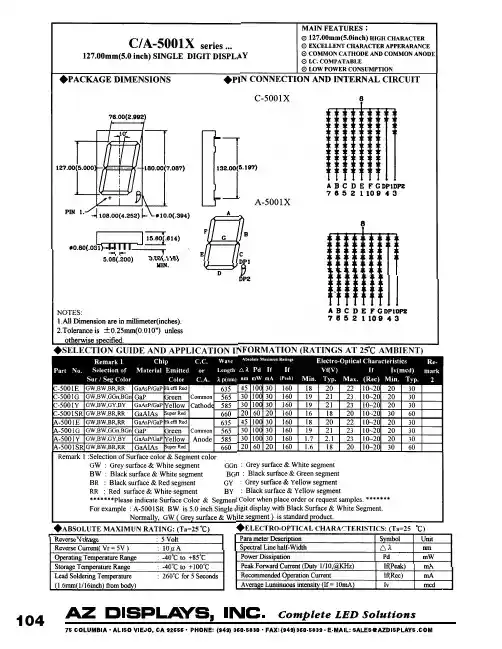
C-5001G中文资料
- 格式:pdf
- 大小:98.15 KB
- 文档页数:1
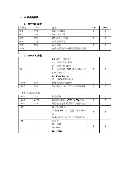
一.16系统类参数1.SETTING 参数参数号 符号 意义 16-T 16-M 0/0 TVC 代码竖向校验 O O 0/1 ISO EIA/ISO代码 O O 0/2 INI MDI方式公/英制 O O 0/5 SEQ 自动加顺序号 O O 2/0 RDG 远程诊断 O O 3216 自动加程序段号时程序段号的间隔O O2.RS232C口参数20 I/O通道(接口板):0,1: 主CPU板JD5A2: 主CPU板JD5B3: 远程缓冲JD5C或选择板1的JD6A(RS-422)5: Data Server10 :DNC1/DNC2接口O O100/3 NCR 程序段结束的输出码 O O 100/5 ND3 DNC运行时:读一段/读至缓冲器满 O OI/O 通道0的参数:101/0 SB2 停止位数 O O 101/3 ASII 数据输入代码:ASCII或EIA/ISO O O 101/7 NFD 数据输出时数据后的同步孔的输出O O 102 输入输出设备号:0:普通RS-232口设备(用DC1-DC4码)3:Handy File(3″软盘驱动器)O O103 波特率:10:480011:960012:19200O O1001/0 INM 公/英制丝杠 O O 1002/2 SFD 是否移动参考点O O 1002/3 AZR 未回参考点时是否报警(#90号) O 1006/0,1 ROT,ROS 设定回转轴和回转方式 O O 1006/3 DIA 指定直径/半径值编程 O 1006/5 ZMI 回参考点方向O O 1007/3 RAA 回转轴的转向(与1008/1:RAB 合用) O O 1008/0 ROA 回转轴的循环功能O O 1008/1 RAB 绝对回转指令时,是否近距回转 O O 1008/2 RRL 相对回转指令时是否规算 O O 1260 回转轴一转的回转量 O O1010 CNC 的控制轴数(不包括PMC 轴) O O 1020 各轴的编程轴名 O O 1022 基本坐标系的轴指定 O O 1023 各轴的伺服轴号 O O 1410 空运行速度 O O 1420 快速移动(G00)速度 O O 1421 快速移动倍率的低速(Fo) O O 1422 最高进给速度允许值(所有轴一样) O O 1423 最高进给速度允许值(各轴分别设) O O 1424 手动快速移动速度 O O 1425 回参考点的慢速 FLO O 1620 快速移动G00时直线加减速时间常数 O O 1622 切削进给时指数加减速时间常数 O O 1624 JOG 方式的指数加减速时间常数 O O 1626 螺纹切削时的加减速时间常数 O 1815/1 OPT 用分离型编码器 O O 1815/5APC 用绝对位置编码器 O O 1816/4,5,6DM1--3 检测倍乘比DMR O O 1820指令倍乘比CMROOI/O 通道1的参数: 111/0 SB2 停止位数O O 111/3 ASI 数据输入代码:ASCII 或EIA/ISO O O 111/7 NFD 数据输出时数据后的同步孔的输出 O O 112输入输出设备号: 0:普通RS-232口设备(用DC1-DC4码)3:Handy File(3″软盘驱动器) OO113波特率:10:480011:9600 12:19200O O其它通道参数请见参数说明书。
B* $ $ & $ % $ +, -# $. / & / & 0 $" 1 . " # $. / & 0 $" 2 . " 0 $" 0 0 0 3 ' 4 0 5 0 $" /6360 7& $" / 8 9: ; 5 7 : </ & # $. * $ ! " 6 3 ! " $ < $& $ $ 9=>2> ? ;5 7 * $ 0 $" 9 ; 5 7 0 0 # $. / & 7 /$ 2 . " 0 $" 5@7 8 $ " $ /$ " < A ! $" $ /$ "< A: B $ $ $ $ $ + $ $ $ $ 4 $元器件交易网0.010.11.0100.20.6 1.0 1.4I ,I N S T A N T A N E O U S F O R W A R D C U R R E N T (A )F V ,INSTANTANEOUS FORWARD VOLTAGE (V)Fig.2Typical Forward Characteristics , per elementF 01020304050110100I ,P E A K F O R W A R D S U R G E C U R R E N T (A )F S M NUMBER OF CYCLES AT 60Hz Fig.3Max Non-Repetitive SurgeCurrent110100110100C ,J U N C T I O N C A P A C I T A N C E (p F )j V ,REVERSE VOLTAGE (V)Fig.4Typical Junction CapacitanceR 00.51.01.50255010012515075I ,A V E R A G E F O R W A R D C U R R E N T (A )F T ,AMBIENT TEMPERATURE (°C)Fig.1Forward Current Derating CurveAB元器件交易网DISCLAIMER :1- The information given herein, including the specifications and dimensions, is subject to change without prior not ice to improveproduct characteristics. Before ordering, purchasers are advised to contact the Sensitron Semiconductor sales department for the latest version of the datasheet(s).2- In cases where extremely high reliability is required (such as use in nuclear power control, aerospace and aviation, traffic equipment, medical equipment , and safety equipment) , safety should be ensured by using semiconductor devices that feature assured safety or by means of users’ fail-safe precautions or other arrangement .3- In no event shall Sensitron Semiconductor be liable for any damages that may result from an accident or any other cause during operation of the user’s units according to the datasheet(s). Sensitron Semiconductor assumes no responsibility for any intellectualproperty claims or any other problems that may result from applications of information, products or circuits described in the datasheets. 4- In no event shall Sensitron Semiconductor be liable for any failure in a semiconductor device or any secondary damage resulting from use at a value exceeding the absolute maximum rating.5- No license is granted by the datasheet(s) under any patents or other rights of any third party or Sensitron Semiconductor.6- The datasheet(s) may not be reproduced or duplicated, in any form, in whole or part, without the expressed written permission of Sensitron Semiconductor.7- The products (technologies) described in the datasheet(s) are not to be provided to any party whose purpose in their application will hinder maintenance of international peace and safety nor are they to be applied to that purpose by their direct purchasers or any third party. When exporting these products (technologies), the necessary procedures are to be taken in accordance with related laws and regulations.SENSITRON SEMICONDUCTOR• ! ! !! "#$ • • % & ' (& ) *+,,---. & ./ 0 • 1 2 &% # % 3 & ./ 0 •B元器件交易网。
TC500/A/510/514Features:•Precision (up to 17 bits) A/D Converter “Front End”•3-Pin Control Interface to Microprocessor •Flexible: User Can Trade-off Conversion Speed for Resolution•Single-Supply Operation (TC510/TC514)• 4 Input, Differential Analog MUX (TC514)•Automatic Input Voltage Polarity Detection •Low Power Dissipation:-(TC500/TC500A): 10mW-(TC510/TC514): 18mW•Wide Analog Input Range:-±4.2V (TC500A/TC510)•Directly Accepts Bipolar and DifferentialInput SignalsApplications:•Precision Analog Signal Processor •Precision Sensor Interface•High Accuracy DC Measurements General Description:TheTC500/A/510/514 family are precision analog front ends that implement dual slope A/D converters having a maximum resolution of 17 bits plus sign. As a minimum, each device contains the integrator, zero crossing comparator and processor interface logic. The TC500 is the base (16-bit max) device and requires both positive and negative power supplies. The TC500A is identical to the TC500 with the exception that it has improved linearity, allowing it to operate to a maximum resolution of 17 bits. The TC510 adds an on-board negative power supply converter for single-supply operation. The TC514 adds both a negative power supply converter and a 4-input differential analog multiplexer.Each device has the same processor control interface consisting of 3 wires: control inputs (A and B) and zero-crossing comparator output (CMPTR). The processor manipulates A, B to sequence the TC5XX through four phases of conversion: auto-zero, integrate, de-integrate and integrator zero. During the auto-zero phase, offset voltages in the TC5XX are corrected by a closed loop feedback mechanism. The input voltage is applied to the integrator during the integrate phase. This causes an integrator output dv/dt directly proportional to the magnitude of the input voltage. The higher the input voltage, the greater the magnitude of the voltage stored on the integrator during this phase. At the start of the de-integrate phase, an external voltage reference is applied to the integrator and, at the same time, the external host processor starts its on-board timer. The processor maintains this state until a transition occurs on the CMPTR output, at which time the processor halts its timer. The resulting timer count is the converted analog data. Integrator zero (the final phase of conversion) removes any residue remaining in the integrator in preparation for the next conversion. The TC500/A/510/514 offer high resolution (up to 17bits), superior 50/60Hz noise rejection, low-power operation, minimum I/O connections, low input bias currents and lower cost compared to other converter technologies having similar conversion speeds.Precision Analog Front Ends with Dual Slope ADC© 2008 Microchip Technology Inc.DS21428E-page 1TC500/A/510/514DS21428E-page 2© 2008 Microchip Technology Inc.Package TypesTypical Application12341615141356712111098CMPTR OUTADGND BV DD V IN +V IN –V REF +BUF V SS C INT ACOM V REF −C REF +C REF –C AZ TC500/TC500A 16-Pin PDIP/SOIC/CERDIPV OUT –1234201918CAP–56781723222191011122425262728DGND A B C REF –C INT C AZ BUF ACOM CH4–CH3–CH2–TC514C REF +V REF –V REF + V DD OSC CMPTR OUTCAP+ 16151314CH1–N/CCH1+CH2+CH3+CH4+A0A128-Pin PDIP/SOIC24-Pin PDIP/SOIC123416151456781319181791011122021222324TC510CAP–DGND A B V DD OSC CMPTR OUT V IN +V IN –N/C N/CCAP+ C REF –C INT C AZ BUF ACOM N/C N/C N/C V OUT –C REF +V REF –V REF +Level Shift Control Logic Analog Switch Control SignalsACOMV REF +BUFC AZBuffer Integrator SW R SW IZ CMPTR 1CMPTR 2CMPTROutputDGNDControl LogicSW 1TC500TC500A TC510TC514C REFC REF +SW RC REF -C AZ R INT C INTC INTSW RI -SW RI -SW RI +SW RI -SW ZSW ISW ZV SS OSC+++Phase Decoding LogicPolarity DetectionDC-TO-DC Converter (TC510 & TC514)-+A B0 0 Zero Integrator Output 0 1 Auto-Zero 1 0 Signal Integrate 1 1 De-integrateV REF -V OUT -C OUT -1.0μF1.0μFV SS SW IB A A0A1DIF.MUX (TC514)CH1+CH2+CH3+CH4+CH1-CH2-CH3-CH4-CAP-CAP+(TC500TC500A)Converter SateTC500/A/510/5141.0ELECTRICALCHARACTERISTICSAbsolute Maximum Ratings†TC510/TC514 Positive Supply Voltage(V DD to GND).........................................+10.5V TC500/TC500A Supply Voltage(V DD to V SS)..............................................+18V TC500/TC500A Positive Supply Voltage(V DD to GND)............................................+12V TC500/TC500A Negative Supply Voltage(V SS to GND)................................................-8V Analog Input Voltage (V IN+ or V IN-)............V DD to V SS Logic Input Voltage...............V DD +0.3V to GND - 0.3V Voltage on OSC: ........................... -0.3V to (V DD +0.3V) for V DD < 5.5V Ambient Operating Temperature Range: ................................................................0°C to +70°C Storage Temperature Range:.............-65°C to +150°C † Notice: Stresses above those listed under “Absolute Maximum Ratings” may cause permanent damage to the device. These are stress ratings only and functional operation of the device at these or any other conditions above those indicated in the operation sections of the specifications is not implied. Exposure to Absolute Maximum Rating conditions for extended periods may affect device reliability.DC CHARACTERISTICSElectrical Specifications: Unless otherwise specified, TC510/TC514: V DD = +5V, TC500/TC500A: V SS= ±5V.C AZ = C REF = 0.47μF.Parameters SymT A = +25°C T A = 0°C to 70°CUnits Conditions Min.Typ.Max.Min.Typ.Max.AnalogResolution60——— — —μV Note1Zero-scale Error with Auto-zero Phase ZSE——0.005—0.0050.012 % F.S.TC500/TC510/TC514——0.003— 0.0030.009TC500AEnd Point Linearity ENL—0.0050.015—0.0150.060% F.S.TC500/TC510/TC514——0.010—0.0100.045% F.S.Note1, Note2,TC500ABest-Case Straight Line Linearity NL—0.0030.008——— % F.S.TC500/TC510/TC514,Note1, Note2——0.005——— % F.S.TC500AZero-scale Temp. Coefficient ZS TC————12μV/°C Over OperatingTemperature RangeFull-scale SymmetryError (Rollover Error)SYE—0.01— — 0.03—% F.S.Note1Full-scale Temperature Coefficient FS TC——— — 10— ppm/°C Over OperatingTemperature Range;External ReferenceTC = 0 ppm/°CInput Current I IN—6————pA V IN = 0VCommon ModeVoltage RangeV CMR V SS + 1.5—V DD – 1.5V SS + 1.5—V DD – 1.5VIntegrator OutputSwingV SS + 0.9—V DD – 0.9V SS + 0.9—V SS + 0.9VAnalog Input SignalRangeV SS + 1.5—V DD – 1.5V SS + 1.5—V SS + 1.5V ACOM = GND = 0VNote1:Integrate time ≥ 66ms, auto-zero time ≥ 66ms, V INT (peak) ≈ 4V.2:End point linearity at ±1/4, ±1/2, ±3/4 F.S. after full-scale adjustment.3:Rollover error is related to C INT, C REF, C AZ characteristics.© 2008 Microchip Technology Inc.DS21428E-page 3TC500/A/510/514DS21428E-page 4© 2008 Microchip Technology Inc.Voltage Reference Range V REFV SS +1—V DD – 1V SS +1—V DD – 1VV REF - V REF +DigitalComparator Logic 1, Output HighV OH 4——4 — —V I SOURCE = 400μA Comparator Logic 0, Output Low V OL ——0.4— — 0.4V I SINK = 2.1mALogic 1, Input High VoltageV IH 3.5—— 3.5——V Logic 0, Input Low VoltageV IL ——1— — 1VLogic Input Current I L ———— 0.3μALogic ‘1’ or ‘0’Comparator Delay t D—2—— 3—μsMultiplexer (TC514 Only)Maximum Input Voltage-2.5— 2.5-2.5—2.5V V DD = 5V Drain/Source ON Resistance R DSON—610— — —k ΩV DD = 5VPower (TC510/TC514 Only)Supply Current I S — 1.8 2.4——3.5mA V DD = 5V, A = 1, B = 1Power Dissipation P D —18—— — —mW V DD = 5VPositive Supply Operating Voltage RangeV DD4.5—5.54.5 —5.5VOperating Source ResistanceR OUT—6085— — 100ΩI OUT = 10mA Oscillator Frequency —100————kHz Note 1Maximum Current OutI OUT ——-10— —-10mAV DD = 5VPower (TC500/TC500A Only)Supply Current I S —1 1.5——2.5mA V S = ±5V, A = B = 1Power Dissipation P D —10—— — —mW V DD = 5V, V SS = -5VPositive Supply Operating Range V DD 4.5—7.5 4.5 —7.5V Negative Supply Operating Range V SS-4.5—-7.5- 4.5—-7.5VDC CHARACTERISTICS (CONTINUED)Electrical Specifications: Unless otherwise specified, TC510/TC514: V DD = +5V, TC500/TC500A : V SS = ±5V. C AZ = C REF = 0.47μF.Parameters SymT A = +25°CT A = 0°C to 70°C Units Conditions Min.Typ.Max.Min.Typ.Max.Note 1:Integrate time ≥ 66ms, auto-zero time ≥ 66ms, V INT (peak) ≈ 4V.2:End point linearity at ±1/4, ±1/2, ±3/4 F.S. after full-scale adjustment.3:Rollover error is related to C INT , C REF , C AZ characteristics.TC500/A/510/514 2.0TYPICAL PERFORMANCE CURVESFIGURE 2-1:Output Voltage vs. Load Current.FIGURE 2-2:Output Ripple vs. Load Current.FIGURE 2-3:Oscillator Frequency vs. Capacitance.FIGURE 2-4:Output Voltage vs. Output Current.FIGURE 2-5:Output Source Resistance vs. Temperature.FIGURE 2-6:Oscillator Frequency vs. Temperature.Note:The graphs and tables provided following this note are a statistical summary based on a limited number of samples and are provided for informational purposes only. The performance characteristics listed herein are not tested or guaranteed. In some graphs or tables, the data presented may be outside the specified operating range (e.g., outside specified power supply range) and therefore outside the warranted range.© 2008 Microchip Technology Inc.DS21428E-page 5TC500/A/510/514NOTES:DS21428E-page 6© 2008 Microchip Technology Inc.TC500/A/510/5143.0PIN DESCRIPTIONSThe descriptions of the pins are listed in Table3-1.TABLE 3-1:PIN FUNCTION TABLETC500,TC510TC514Symbol Function TC500ACERDIP,PDIP, SOIC PDIP, SOICPDIP, SOIC122C INT Integrator output. Integrator capacitor connection.2Not Used Not Used V SS Negative power supply input (TC500/TC500A only).333C AZ Auto-zero input. The auto-zero capacitor connection.444BUF Buffer output. The Integrator capacitor connection.555ACOM This pin is grounded in most applications. It is recommended thatACOM and the input common pin (Ve n- or CH n-) be within the analogCommon Mode Range (CMR).666C REF-Input. Negative reference capacitor connection.777C REF+Input. Positive reference capacitor connection.888V REF-Input. External voltage reference (-) connection.999V REF+Input. External voltage reference (+) connection.1015Not Used V IN-Negative analog input.1116Not Used V IN+Positive analog input.121822A Input. Converter phase control MSB. (See input B.)131721B Input. Converter phase control LSB. The states of A, B place theTC5XX in one of four required phases. A conversion is completewhen all four phases have been executed:Phase control input pins:AB = 00: Integrator zero01: Auto-zero10: Integrate11: De-integrate 141923CMPTR OUT Zero crossing comparator output. CMPTR is high during theintegration phase when a positive input voltage is being integratedand is low when a negative input voltage is being integrated. A high-to-low transition on CMPTR signals the processor that the De-integrate phase is completed. CMPTR is undefined during the auto-zero phase. It should be monitored to time the integrator zero phase.152327DGND Input. Digital ground.162125V DD Input. Power supply positive connection.—2226CAP+Input. Negative power supply converter capacitor (+) connection.—2428CAP-Input. Negative power supply converter capacitor (-) connection.—11V OUT-Output. Negative power supply converter output and reservoircapacitor connection. This output can be used to power otherdevices in the circuit requiring a negative bias voltage.—2024OSC Oscillator control input. The negative power supply converternormally runs at a frequency of 100kHz. The converter oscillatorfrequency can be slowed down (to reduce quiescent current) byconnecting an external capacitor between this pin and V DD (seeSection2.0 “Typical Performance Curves”).——18 CH1+Positive analog input pin. MUX channel 1.——13CH1-Negative analog input pin. MUX channel 1.——17CH2+Positive analog input pin. MUX channel 2.——12CH2-Negative analog input pin. MUX channel 2.——16CH3+Positive analog input pin. MUX channel 3.——11CH3-Negative analog input pin. MUX channel 3.——15CH4+Positive analog input pin. MUX channel 4.——10CH4-Negative analog input pin. MUX channel 4——20A0Multiplexer input channel select input LSB (see A1).© 2008 Microchip Technology Inc.DS21428E-page 7TC500/A/510/514DS21428E-page 8© 2008 Microchip Technology Inc.——19A1Multiplexer input channel select input MSB.Phase control input pins: A1, A0 =00 = Channel 101 = Channel 210 = Channel 311 = Channel 4TABLE 3-1:PIN FUNCTION TABLE (CONTINUED)TC500, TC500ATC510TC514Symbol FunctionCERDIP ,PDIP , SOICPDIP , SOICPDIP , SOIC© 2008 Microchip Technology Inc.DS21428E-page 9TC500/A/510/5144.0DETAILED DESCRIPTION4.1Dual Slope Conversion PrinciplesActual data conversion is accomplished in two phases: input signal integration and reference voltage de-integration.The integrator output is initialized to 0V prior to the start of integration. During integration, analog switch S 1connects V IN to the integrator input where it is maintained for a fixed time period (T INT ). The application of V IN causes the integrator output to depart 0V at a rate determined by the magnitude of V IN and a direction determined by the polarity of V IN . The de-integration phase is initiated immediately at the expiration of T INT .During de-integration, S1 connects a reference voltage (having a polarity opposite that of V IN ) to the integrator input. At the same time, an external precision timer is started. The de-integration phase is maintained until the comparator output changes state, indicating the integrator has returned to its starting point of 0V. When this occurs, the precision timer is stopped. The de-integration time period (T DEINT ), as measured by the precision timer, is directly proportional to the magnitude of the applied input voltage (see Figure 4-3).A simple mathematical equation relates the input signal, reference voltage and integration time:EQUATION 4-1:For a constant V IN :EQUATION 4-2:The dual slope converter accuracy is unrelated to the integrating resistor and capacitor values as long as they are stable during a measurement cycle.An inherent benefit is noise immunity. Input noise spikes are integrated (averaged to zero) during the integration periods. Integrating ADCs are immune to the large conversion errors that plague successive approximation converters in high noise environments.Integrating converters provide inherent noise rejection with at least a 20dB/decade attenuation rate.Interference signals with frequencies at integral multiples of the integration period are, theoretically,completely removed, since the average value of a sine wave of frequency (1/T) averaged over a period (T) is zero.Integrating converters often establish the integration period to reject 50/60 Hz line frequency interference signals. The ability to reject such signals is shown by a normal mode rejection plot (Figure 4-1). Normal mode rejection is limited in practice to 50 to 65dB, since the line frequency can deviate by a few tenths of a percent (Figure 4-2).Normal Mode Rejection.Where:V REF =Reference VoltageT INT =Signal Integration time (fixed)t DEINT=Reference Voltage Integration time(variable)1R INT C INT -----------------------V IN T ()DT 0T INT ∫V REF C DEINT R INT C INT--------------------------------=V INV REF T DEINTT INT-----------------=TC500/A/510/514DS21428E-page 10© 2008 Microchip Technology Inc.FIGURE 4-3:Basic Dual Slope Converter.Phase ControlComparatorI n t e g r a t o r O u t p u tIntegrator C INTAnalog Input (V IN )Switch Driver Ref VoltageControl LogicPolarity Control S 1I/OTimer CounterROM RAMMicrocomputer AB CMPTR OutV SUPPLY ±T INTTC510V INTV IN ≈ V REFV IN ≈ 1/2 V REFT DEINT–+R INTV INT–+分销商库存信息:MICROCHIPTC510COG TC500CPE TC500COE TC500COE713TC510COG713TC514CPJTC514COI TC514COI713TC510EOG713 TC500IJE TC510CPF。