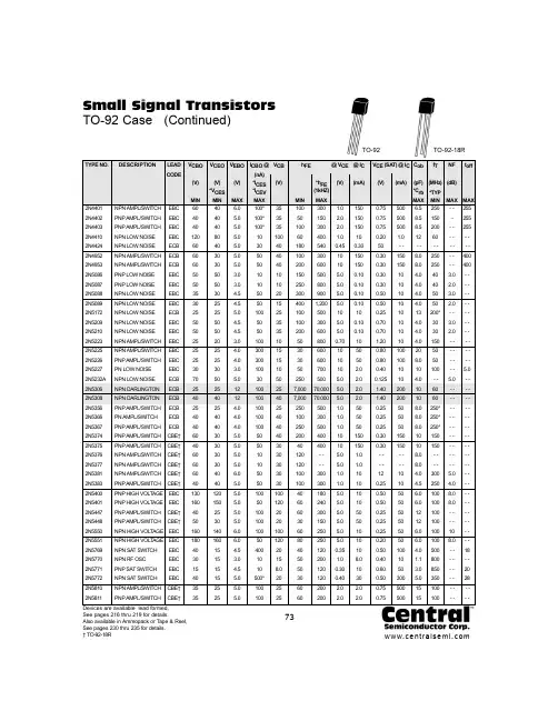
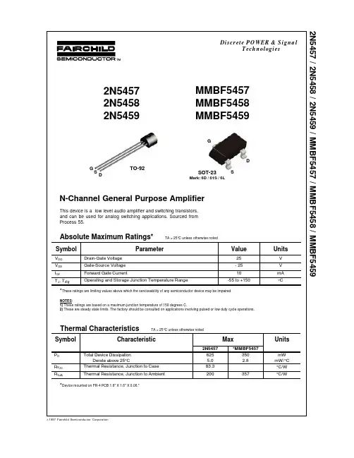
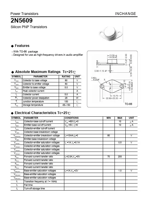
2N5089中文资料
- 格式:pdf
- 大小:157.16 KB
- 文档页数:8
Amplifier TransistorsNPN SiliconMAXIMUM RATINGSTHERMAL CHARACTERISTICSELECTRICAL CHARACTERISTICS (T = 25°C unless otherwise noted)OFF CHARACTERISTICS1.R θJA is measured with the device soldered into a typical printed circuit board.2.Pulse Test: Pulse Width ≤ 300 m s, Duty Cycle ≤ 2.0%.ON Semiconductor t© Semiconductor Components Industries, LLC, 20011Publication Order Number:2N50882N5089COLLECTOR21EMITTERELECTRICAL CHARACTERISTICS (T= 25°C unless otherwise noted) (Continued)SMALL–SIGNAL CHARACTERISTICS2.Pulse Test: Pulse Width ≤ 300 m s, Duty Cycle ≤ 2.0%.Figure 2. Effects of Frequencyf, FREQUENCY (Hz)7.01020305.0Figure 3. Effects of Collector CurrentI C , COLLECTOR CURRENT (mA)Figure 4. Noise Currentf, FREQUENCY (Hz)Figure 5. Wideband Noise FigureR S , SOURCE RESISTANCE (OHMS)3.0NOISE CHARACTERISTICS(V CE = 5.0 Vdc, T A = 25°C)NOISE VOLTAGEe n , N O I S E V O L T A G E (n V )e n , N O IS E V O L T A G E (n V )I n , N O I S E C U R R E N T (p A )N F , N O I S E F I G U R E (d B )7.01020305.03.0100.10.20.31.00.72.03.05.07.004.08.0121620100 Hz NOISE DATA3002001003.05.07.010********R S , SOURCE RESISTANCE (OHMS)V T , T O T A L N O I S E V O L T A G E (n V )N F , N O I S E F I G U R E (d B )4.08.01220Figure 6. Total Noise Voltage R S , SOURCE RESISTANCE (OHMS)Figure 7. Noise Figure0.5Figure 8. DC Current GainI C , COLLECTOR CURRENT (mA)0.41.02.03.04.00.3h , D C C U R R E N T G A I N (N O R M A L I Z E D )0.2F E 0.70.5Figure 9. “On” VoltagesI C , COLLECTOR CURRENT (mA)0.40.60.81.00.2Figure 10. Temperature CoefficientsI C , COLLECTOR CURRENT (mA)V , V O L T A G E (V O L T S )-ā0.8-ā1.2-ā1.6-ā2R V B E ,B A S E -E M I T T E R θT E M P ER A T U R E C O E F F I C I E N T (m V /C )°-ā0.4-ā2.0f T , C U R R E N T -G A I N Ċ B A N D W I D T H P R O D U C T (M H z )C , C A P A C I T A N C E (p F )8.00.81.02.03.04.06.05003002007050100Figure 11. Capacitance V R , REVERSE VOLTAGE (VOLTS)Figure 12. Current–Gain — Bandwidth ProductI C , COLLECTOR CURRENT (mA)PACKAGE DIMENSIONSCASE 29–11ISSUE ALTO–92 (TO–226)NOTES:1.DIMENSIONING AND TOLERANCING PER ANSI Y14.5M, 1982.2.CONTROLLING DIMENSION: INCH.3.CONTOUR OF PACKAGE BEYOND DIMENSION R IS UNCONTROLLED.4.LEAD DIMENSION IS UNCONTROLLED IN P AND BEYOND DIMENSION K MINIMUM.PLANEDIM MIN MAX MIN MAX MILLIMETERSINCHES A 0.1750.205 4.45 5.20B 0.1700.210 4.32 5.33C 0.1250.165 3.18 4.19D 0.0160.0210.4070.533G 0.0450.055 1.15 1.39H 0.0950.105 2.42 2.66J 0.0150.0200.390.50K 0.500---12.70---L 0.250--- 6.35---N 0.0800.105 2.04 2.66P ---0.100--- 2.54R 0.115--- 2.93---V0.135--- 3.43---EMITTER2.BASE3.COLLECTORON Semiconductor and are trademarks of Semiconductor Components Industries, LLC (SCILLC). SCILLC reserves the right to make changes without further notice to any products herein. SCILLC makes no warranty, representation or guarantee regarding the suitability of its products for any particular purpose, nor does SCILLC assume any liability arising out of the application or use of any product or circuit, and specifically disclaims any and all liability, including without limitation special, consequential or incidental damages. “Typical” parameters which may be provided in SCILLC data sheets and/or specifications can and do vary in different applications and actual performance may vary over time. All operating parameters, including “Typicals” must be validated for each customer application by customer’s technical experts. SCILLC does not convey any license under its patent rights nor the rights of others.SCILLC products are not designed, intended, or authorized for use as components in systems intended for surgical implant into the body, or other applications intended to support or sustain life, or for any other application in which the failure of the SCILLC product could create a situation where personal injury or death may occur. Should Buyer purchase or use SCILLC products for any such unintended or unauthorized application, Buyer shall indemnify and hold SCILLC and its officers, employees, subsidiaries, affiliates, and distributors harmless against all claims, costs, damages, and expenses, and reasonable attorney fees arising out of, directly or indirectly, any claim of personal injury or death associated with such unintended or unauthorized use, even if such claim alleges that SCILLC was negligent regarding the design or manufacture of the part. SCILLC is an Equal Opportunity/Affirmative Action Employer. PUBLICATION ORDERING INFORMATIONJAPAN: ON Semiconductor, Japan Customer Focus Center4–32–1 Nishi–Gotanda, Shinagawa–ku, Tokyo, Japan 141–0031Phone: 81–3–5740–2700Email: r14525@。