MOSFET隔离型高速驱动电路
- 格式:pdf
- 大小:705.90 KB
- 文档页数:5

隔离mosfet mos管场效应管模块替代继电器电路-概述说明以及解释1.引言1.1 概述隔离MOSFET(MOS管)场效应管模块作为一种新型的电子器件,正在逐渐成为替代传统继电器电路的热门选择。
传统的继电器电路由于存在机械结构,在工作过程中容易产生噪声、寿命短、响应时间长等问题,限制了其在现代电子设备中的应用。
而隔离MOSFET场效应管模块因其具有高速响应、可靠性强、功耗低等特点,逐渐受到了工程师和电子爱好者的青睐。
本文将重点介绍隔离MOSFET(MOS管)和继电器电路的基本原理和特点,分析它们在不同应用场景下的工作原理及优缺点。
通过比较两者的特点,旨在探讨隔离MOSFET(MOS管)作为继电器电路的替代品的可行性和推广性。
本文将分为三个部分来进行阐述:引言、正文和结论。
引言部分概述了文章的主要内容和结构,同时阐述了撰写本文的动机和目的。
正文部分将详细介绍MOSFET(MOS管)和继电器电路的基本原理以及它们的工作原理和应用场景。
结论部分将总结MOSFET(MOS管)在替代继电器电路中的优势,并分析其在实际应用中的可行性和推广性。
通过详细的论述和分析,有助于读者全面了解隔离MOSFET(MOS 管)和继电器电路的不同特点,进而评估隔离MOSFET(MOS管)作为继电器电路的替代品的可行性,并为相关领域的工程师和研究人员提供参考和借鉴。
随着科技的不断发展和进步,寻找更加先进、高效、可靠的电子器件,已经成为了当前电子工程领域的一项重要任务。
1.2文章结构文章结构:本文主要分为引言、正文和结论三个部分。
在引言部分,我们将对本文的概述进行介绍,解释MOSFET (MOS管)和继电器电路的基本概念及其作用。
接着将介绍文章的结构和主要内容,提供给读者一个清晰的整体框架。
最后,说明本文的目的,即研究和探讨隔离MOSFET MOS管场效应管模块替代继电器电路的可行性和优势。
正文部分将主要分为两个章节,第一章节将详细介绍MOSFET (MOS 管)的基本原理和特点,包括其结构、工作原理和优势。
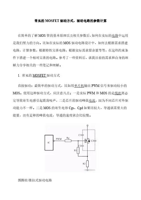
常见的MOSFET驱动方式,驱动电路的参数计算在简单的了解MOS管的基本原理以及相关参数后,如何在实际的电路中运用是我们努力的方向。
比如在实际的MOS驱动电路设计中,如何去根据需求搭建电路,计算参数,根据特性完善电路,根据实际需求留余量等等,在这些约束条件下搭建一个相对完善的电路。
参考了一些资料后,就我目前的需求和自身的理解力分享相关的一些笔记和理解。
1.常见的MOSFET驱动方式直接驱动:最简单的驱动方式,比如用单片机输出PWM信号来驱动较小的MOS。
使用这种驱动方式,应注意几点;一是实际PWM和MOS的走线距离必定导致寄生电感引起震荡噪声,二是芯片的驱动峰值电流,因为不同芯片对外驱动能力不一样。
三是MOS的寄生电容Cgs、Cgd如果比较大,导通就需要大的能量,没有足够的峰值电流,导通的速度就会比较慢。
图腾柱/推拉式驱动电路由两个三极管构成,上管是NPN型,下管是PNP型三极管,两对管共射联接处为输出端,结构类似于乙类推挽功率放大器。
利用这种拓扑放大驱动信号,增强电流能力。
(驱动IC内部也是集成了类似的结构)隔离式驱动电路为了满足安全隔离也会用变压器驱动。
如图其中R1抑制振荡,C1隔直流通交流同时防止磁芯饱和。
隔离式的驱动电路不太常见,就不做过多的了解。
小结:当然除以上驱动电路之外,还有很多其它形式的驱动电路。
对于各种各样的驱动电路并没有一种是最好的,只能结合具体应用,选择最合适的拓扑。
2.驱动电路的参数计算我的实际工作中碰到最多的驱动电路是以下这种能够控制开关速度的驱动电路,我就以它举例做进一步的分析。
如图,在驱动电阻Rg2上并联一个二极管。
其中D1常用快恢复二极管,使关断时间减小同时减小关断损耗,Rg1可以限制关断电流,R1为mos管栅源极的下拉电阻,给mos管栅极积累的电荷提供泄放回路。
(根据MOSFET栅极高输入阻抗的特性,一点点静电或者干扰都可能导致MOS管误导通,所以R1也起降低输入阻抗作用,一般取值在10k~几十k)Lp为驱动走线的杂散寄生电感,包括驱动IC引脚、MOS引脚、PCB走线的感抗,精确的数值很难确定,通常取几十nH。

详细讲解M O S F E T管驱动电路在使用MOS管设计开关电源或者马达驱动电路的时候,大部分人都会考虑MOS的导通电阻,最大电压等,最大电流等,也有很多人仅仅考虑这些因素;这样的电路也许是可以工作的,但并不是优秀的,作为正式的产品设计也是不允许的;下面是我对MOSFET及MOSFET驱动电路基础的一点总结,其中参考了一些资料,非全部原创;包括MOS管的介绍,特性,驱动以及应用电路;1,MOS管种类和结构MOSFET管是FET的一种另一种是JFET,可以被制造成增强型或耗尽型,P沟道或N沟道共4种类型,但实际应用的只有增强型的N沟道MOS管和增强型的P沟道MOS管,所以通常提到NMOS,或者PMOS指的就是这两种;至于为什么不使用耗尽型的MOS管,不建议刨根问底;对于这两种增强型MOS管,比较常用的是NMOS;原因是导通电阻小,且容易制造;所以开关电源和马达驱动的应用中,一般都用NMOS;下面的介绍中,也多以NMOS 为主;MOS管的三个管脚之间有寄生电容存在,这不是我们需要的,而是由于制造工艺限制产生的;寄生电容的存在使得在设计或选择驱动电路的时候要麻烦一些,但没有办法避免,后边再详细介绍;在MOS管原理图上可以看到,漏极和源极之间有一个寄生二极管;这个叫体二极管,在驱动感性负载如马达,这个二极管很重要;顺便说一句,体二极管只在单个的MOS管中存在,在集成电路芯片内部通常是没有的;2,MOS管导通特性导通的意思是作为开关,相当于开关闭合;NMOS的特性,Vgs大于一定的值就会导通,适合用于源极接地时的情况低端驱动,只要栅极电压达到4V或10V就可以了;PMOS的特性,Vgs小于一定的值就会导通,适合用于源极接VCC时的情况高端驱动;但是,虽然PMOS可以很方便地用作高端驱动,但由于导通电阻大,价格贵,替换种类少等原因,在高端驱动中,通常还是使用NMOS;3,MOS开关管损失不管是NMOS还是PMOS,导通后都有导通电阻存在,这样电流就会在这个电阻上消耗能量,这部分消耗的能量叫做导通损耗;选择导通电阻小的MOS管会减小导通损耗;现在的小功率MOS管导通电阻一般在几十毫欧左右,几毫欧的也有;MOS在导通和截止的时候,一定不是在瞬间完成的;MOS两端的电压有一个下降的过程,流过的电流有一个上升的过程,在这段时间内,MOS管的损失是电压和电流的乘积,叫做开关损失;通常开关损失比导通损失大得多,而且开关频率越快,损失也越大;导通瞬间电压和电流的乘积很大,造成的损失也就很大;缩短开关时间,可以减小每次导通时的损失;降低开关频率,可以减小单位时间内的开关次数;这两种办法都可以减小开关损失;4,MOS管驱动跟双极性晶体管相比,一般认为使MOS管导通不需要电流,只要GS电压高于一定的值,就可以了;这个很容易做到,但是,我们还需要速度;在MOS管的结构中可以看到,在GS,GD之间存在寄生电容,而MOS管的驱动,实际上就是对电容的充放电;对电容的充电需要一个电流,因为对电容充电瞬间可以把电容看成短路,所以瞬间电流会比较大;选择/设计MOS管驱动时第一要注意的是可提供瞬间短路电流的大小;第二注意的是,普遍用于高端驱动的NMOS,导通时需要是栅极电压大于源极电压;而高端驱动的MOS管导通时源极电压与漏极电压VCC相同,所以这时栅极电压要比VCC大4V或10V;如果在同一个系统里,要得到比VCC大的电压,就要专门的升压电路了;很多马达驱动器都集成了电荷泵,要注意的是应该选择合适的外接电容,以得到足够的短路电流去驱动MOS管;上边说的4V或10V是常用的MOS管的导通电压,设计时当然需要有一定的余量;而且电压越高,导通速度越快,导通电阻也越小;现在也有导通电压更小的MOS管用在不同的领域里,但在12V汽车电子系统里,一般4V导通就够用了;MOS管的驱动电路及其损失,可以参考Microchip公司的AN799 Matching MOSFET Drivers to MOSFETs;讲述得很详细,所以不打算多写了;5,MOS管应用电路MOS管最显着的特性是开关特性好,所以被广泛应用在需要电子开关的电路中,常见的如开关电源和马达驱动,也有照明调光;现在的MOS驱动,有几个特别的需求,1,低压应用当使用5V电源,这时候如果使用传统的图腾柱结构,由于三极管的be有左右的压降,导致实际最终加在gate上的电压只有;这时候,我们选用标称gate电压的MOS管就存在一定的风险;同样的问题也发生在使用3V或者其他低压电源的场合;2,宽电压应用输入电压并不是一个固定值,它会随着时间或者其他因素而变动;这个变动导致PWM电路提供给MOS管的驱动电压是不稳定的;为了让MOS管在高gate电压下安全,很多MOS管内置了稳压管强行限制gate电压的幅值;在这种情况下,当提供的驱动电压超过稳压管的电压,就会引起较大的静态功耗;同时,如果简单的用电阻分压的原理降低gate电压,就会出现输入电压比较高的时候,MOS管工作良好,而输入电压降低的时候gate电压不足,引起导通不够彻底,从而增加功耗;3,双电压应用在一些控制电路中,逻辑部分使用典型的5V或者数字电压,而功率部分使用12V甚至更高的电压;两个电压采用共地方式连接;这就提出一个要求,需要使用一个电路,让低压侧能够有效的控制高压侧的MOS管,同时高压侧的MOS管也同样会面对1和2中提到的问题;在这三种情况下,图腾柱结构无法满足输出要求,而很多现成的MOS驱动IC,似乎也没有包含gate电压限制的结构;于是我设计了一个相对通用的电路来满足这三种需求;电路图如下:图1 用于NMOS的驱动电路图2 用于PMOS的驱动电路这里我只针对NMOS驱动电路做一个简单分析:Vl和Vh分别是低端和高端的电源,两个电压可以是相同的,但是Vl不应该超过Vh;Q1和Q2组成了一个反置的图腾柱,用来实现隔离,同时确保两只驱动管Q3和Q4不会同时导通;R2和R3提供了aPWM电压基准,通过改变这个基准,可以让电路工作在PWM信号波形比较陡直的位置;Q3和Q4用来提供驱动电流,由于导通的时候,Q3和Q4相对Vh和GND最低都只有一个Vce的压降,这个压降通常只有左右,大大低于的Vce;R5和R6是反馈电阻,用于对gate电压进行采样,采样后的电压通过Q5对Q1和Q2的基极产生一个强烈的负反馈,从而把gate电压限制在一个有限的数值;这个数值可以通过R5和R6来调节;最后,R1提供了对Q3和Q4的基极电流限制,R4提供了对MOS管的gate电流限制,也就是Q3和Q4的Ice的限制;必要的时候可以在R4上面并联加速电容;这个电路提供了如下的特性:1,用低端电压和PWM驱动高端MOS管;2,用小幅度的PWM信号驱动高gate电压需求的MOS管;3,gate电压的峰值限制4,输入和输出的电流限制5,通过使用合适的电阻,可以达到很低的功耗;6,PWM信号反相;NMOS并不需要这个特性,可以通过前置一个反相器来解决;在设计便携式设备和无线产品时,提高产品性能、延长电池工作时间是设计人员需要面对的两个问题;DC-DC转换器具有效率高、输出电流大、静态电流小等优点,非常适用于为便携式设备供电;目前DC-DC转换器设计技术发展主要趋势有:1高频化技术:随着开关频率的提高,开关变换器的体积也随之减小,功率密度也得到大幅提升,动态响应得到改善;小功率DC-DC转换器的开关频率将上升到兆赫级;2低输出电压技术:随着半导体制造技术的不断发展,微处理器和便携式电子设备的工作电压越来越低,这就要求未来的DC-DC变换器能够提供低输出电压以适应微处理器和便携式电子设备的要求;这些技术的发展对电源芯片电路的设计提出了更高的要求;首先,随着开关频率的不断提高,对于开关元件的性能提出了很高的要求,同时必须具有相应的开关元件驱动电路以保证开关元件在高达兆赫级的开关频率下正常工作;其次,对于电池供电的便携式电子设备来说,电路的工作电压低以锂电池为例,工作电压~,因此,电源芯片的工作电压较低;MOS管具有很低的导通电阻,消耗能量较低,在目前流行的高效DC-DC芯片中多采用MOS管作为功率开关;但是由于MOS管的寄生电容大,一般情况下NMOS开关管的栅极电容高达几十皮法;这对于设计高工作频率DC-DC转换器开关管驱动电路的设计提出了更高的要求;在低电压ULSI设计中有多种CMOS、BiCMOS采用自举升压结构的逻辑电路和作为大容性负载的驱动电路;这些电路能够在低于1V电压供电条件下正常工作,并且能够在负载电容1~2pF的条件下工作频率能够达到几十兆甚至上百兆赫兹;本文正是采用了自举升压电路,设计了一种具有大负载电容驱动能力的,适合于低电压、高开关频率升压型DC-DC转换器的驱动电路;电路基于Samsung AHP615 BiCMOS工艺设计并经过Hspice仿真验证,在供电电压,负载电容为60pF时,工作频率能够达到5MHz以上;自举升压电路自举升压电路的原理图如图1所示;所谓的自举升压原理就是,在输入端IN 输入一个方波信号,利用电容Cboot将A点电压抬升至高于VDD的电平,这样就可以在B端输出一个与输入信号反相,且高电平高于VDD的方波信号;具体工作原理如下;当VIN为高电平时,NMOS管N1导通,PMOS管P1截止,C点电位为低电平;同时N2导通,P2的栅极电位为低电平,则P2导通;这就使得此时A点电位约为VDD,电容Cboot两端电压UC≈VDD;由于N3导通,P4截止,所以B点的电位为低电平;这段时间称为预充电周期;当VIN变为低电平时,NMOS管N1截止,PMOS管P1导通,C点电位为高电平,约为VDD;同时N2、N3截止,P3导通;这使得P2的栅极电位升高,P2截止;此时A 点电位等于C点电位加上电容Cboot两端电压,约为2VDD;而且P4导通,因此B点输出高电平,且高于VDD;这段时间称为自举升压周期;实际上,B点电位与负载电容和电容Cboot的大小有关,可以根据设计需要调整;具体关系将在介绍电路具体设计时详细讨论;在图2中给出了输入端IN电位与A、B两点电位关系的示意图;驱动电路结构图3中给出了驱动电路的电路图;驱动电路采用Totem输出结构设计,上拉驱动管为NMOS管N4、晶体管Q1和PMOS管P5;下拉驱动管为NMOS管N5;图中CL为负载电容,Cpar为B点的寄生电容;虚线框内的电路为自举升压电路;本驱动电路的设计思想是,利用自举升压结构将上拉驱动管N4的栅极B点电位抬升,使得UB>VDD+VTH ,则NMOS管N4工作在线性区,使得VDSN4 大大减小,最终可以实现驱动输出高电平达到VDD;而在输出低电平时,下拉驱动管本身就工作在线性区,可以保证输出低电平位GND;因此无需增加自举电路也能达到设计要求;考虑到此驱动电路应用于升压型DC-DC转换器的开关管驱动,负载电容CL很大,一般能达到几十皮法,还需要进一步增加输出电流能力,因此增加了晶体管Q1作为上拉驱动管;这样在输入端由高电平变为低电平时,Q1导通,由N4、Q1同时提供电流,OUT端电位迅速上升,当OUT端电位上升到VDD-VBE时,Q1截止,N4继续提供电流对负载电容充电,直到OUT端电压达到VDD;在OUT端为高电平期间,A点电位会由于电容Cboot 上的电荷泄漏等原因而下降;这会使得B点电位下降,N4的导通性下降;同时由于同样的原因,OUT端电位也会有所下降,使输出高电平不能保持在VDD;为了防止这种现象的出现,又增加了PMOS管P5作为上拉驱动管,用来补充OUT端CL的泄漏电荷,维持OUT端在整个导通周期内为高电平;驱动电路的传输特性瞬态响应在图4中给出;其中a为上升沿瞬态响应,b为下降沿瞬态响应;从图4中可以看出,驱动电路上升沿明显分为了三个部分,分别对应三个上拉驱动管起主导作用的时期;1阶段为Q1、N4共同作用,输出电压迅速抬升,2阶段为N4起主导作,使输出电平达到VDD,3阶段为P5起主导作用,维持输出高电平为VDD;而且还可以缩短上升时间,下降时间满足工作频率在兆赫兹级以上的要求;需要注意的问题及仿真结果电容Cboot的大小的确定Cboot的最小值可以按照以下方法确定;在预充电周期内,电容Cboot 上的电荷为VDDCboot ;在A点的寄生电容计为CA上的电荷为VDDCA;因此在预充电周期内,A点的总电荷为Q_{A1}=V_{DD}C_{boot}+V_{DD}C_{A} 1B点电位为GND,因此在B点的寄生电容Cpar上的电荷为0;在自举升压周期,为了使OUT端电压达到VDD,B点电位最低为VB=VDD+Vthn;因此在B点的寄生电容Cpar上的电荷为Q_{B}=V_{DD}+V_{thn}Cpar 2忽略MOS管P4源漏两端压降,此时Cboot上的电荷为VthnCboot ,A点寄生电容CA的电荷为VDD+VthnCA;A点的总电荷为QA2=V_{thn}C_{BOOT}+V_{DD}+V_{thn}C_{A} 3同时根据电荷守恒又有Q_{B}=Q_{A}-Q_{A2} 4综合式1~4可得C_{boot}=\frac{V_{DD}+V_{thn}}{v_{DD}-v_{thn}}Cpar+\frac{v_{thn}}{v_{DD}-v_{ thn}}C_{A}=\frac{V_{B}}{v_{DD}-v_{thn}}Cpar+\frac{V_{thn}}{v_{DD}-v_{thn}}C_{ A} 5从式5中可以看出,Cboot随输入电压变小而变大,并且随B点电压VB变大而变大;而B点电压直接影响N4的导通电阻,也就影响驱动电路的上升时间;因此在实际设计时,Cboot的取值要大于式5的计算结果,这样可以提高B点电压,降低N4导通电阻,减小驱动电路的上升时间;P2、P4的尺寸问题将公式5重新整理后得:V_{B}={V_{DD}-V_{thn}\frac{C_{boot}}{Cpar}-V_{thn}\frac{C_{A}}{Cpar} 6 从式6中可以看出在自举升压周期内, A、B两点的寄生电容使得B点电位降低;在实际设计时为了得到合适的B点电位,除了增加Cboot大小外,要尽量减小A、B两点的寄生电容; 在设计时,预充电PMOS管P2的尺寸尽可能的取小,以减小寄生电容CA;而对于B点的寄生电容Cpar来说,主要是上拉驱动管N4的栅极寄生电容,MOS管P4、N3的源漏极寄生电容只占一小部分;我们在前面的分析中忽略了P4的源漏电压,因此设计时就要尽量的加大P4的宽长比,使其在自举升压周期内的源漏电压很小可以忽略;但是P4的尺寸以不能太大,要保证P4的源极寄生电容远远小于上拉驱动管N4的栅极寄生电容;阱电位问题如图3所示,PMOS器件P2、P3、P4的N-well连接到了自举升压节点A上;这样做的目的是,在自举升压周期内,防止他们的源/漏--阱结导通;而且这还可以防止在源/漏--阱正偏时产生由寄生SRC引起的闩锁现象;上拉驱动管N4的阱偏置电位要接到它的源极,最好不要直接接地;这样做的目的是消除衬底偏置效应对N4的影响;Hspice仿真验证结果驱动电路基于Samsung AHP615 BiCMOS工艺设计并经过Hspice仿真验证;在表1中给出了电路在不同工作电压、不同负载条件下的上升时间tr和下降时间tf 的仿真结果;在图5中给了电路工作在输入电压、工作频率为5MHz、负载电容60pF条件下的输出波形;结合表1和图5可以看出,此驱动电路能够在工作电压为,工作频率为5MHz,并且负载电容高达60pF的条件下正常工作;它可以应用于低电压、高工作频率的DC-DC转换器中作为开关管的驱动电路;结论本文采用自举升压电路,设计了一种BiCMOS Totem结构的驱动电路;该电路基于Samsung AHP615 BiCMOS工艺设计,可在电压供电条件下正常工作,而且在负载电容为60pF的条件下,工作频率可达5MHz以上;。

mosfet电压隔离驱动方案MOSFET电压隔离驱动方案随着现代电子技术的快速发展,电路的稳定性和可靠性要求也越来越高。
在一些特殊的应用场景中,如高频电路、高压电路、噪声环境下的电路等,需要对电路进行电压隔离来提高系统的稳定性和安全性。
MOSFET电压隔离驱动方案因其高速、低功耗和可靠性等优势,成为了一种常用的解决方案。
MOSFET(金属氧化物半导体场效应晶体管)是一种常见的半导体器件,具有高速开关和低功耗的特点。
通过控制MOSFET的栅极电压,可以实现对电路的开关控制。
而MOSFET电压隔离驱动方案则是利用MOSFET的特性来实现电路之间的电压隔离。
在MOSFET电压隔离驱动方案中,一般会使用光耦来实现电路间的隔离。
光耦是一种能够将电路间的信号通过光信号进行转换的器件。
它由发光二极管(LED)和光敏二极管(光电晶体管)组成。
当输入信号施加在发光二极管上时,发光二极管会发出光信号,光信号经过隔离区域后,被光敏二极管接收并转换为与输入信号相同的电信号。
通过光耦将输入信号与MOSFET的栅极连接起来,当输入信号施加在光耦上时,光敏二极管会产生相应的电信号,通过MOSFET的栅极电压来控制MOSFET的导通和关断。
由于光耦实现了输入信号和MOSFET之间的电气隔离,可以有效地提高系统的稳定性和安全性。
MOSFET电压隔离驱动方案具有以下几个优势:1. 高速开关:MOSFET具有快速的开关速度,可以实现高频电路的要求。
通过光耦隔离驱动MOSFET,可以实现输入信号的快速响应,提高系统的响应速度。
2. 低功耗:MOSFET的工作电流较小,具有较低的功耗。
通过光耦隔离驱动MOSFET,可以进一步降低功耗,提高系统的能效。
3. 可靠性高:MOSFET具有较高的可靠性,长时间工作不易出现故障。
通过光耦隔离驱动MOSFET,可以避免外部电源的电压干扰和噪声对系统的影响,提高系统的稳定性和可靠性。
4. 成本低:MOSFET电压隔离驱动方案相对于其他电压隔离方案来说,成本较低。
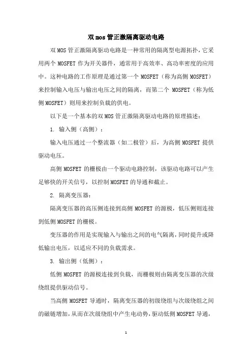
双mos管正激隔离驱动电路双MOS管正激隔离驱动电路是一种常用的隔离型电源拓扑,它采用两个MOSFET作为开关器件,通常用于高效率、高功率密度的应用中。
这种电路的工作原理是通过第一个MOSFET(称为高侧MOSFET)来控制输入电压与输出电压之间的隔离,而第二个MOSFET(称为低侧MOSFET)则用来控制负载的供电。
以下是一个基本的双MOS管正激隔离驱动电路的原理描述:1. 输入侧(高侧):输入电压通过一个整流器(如二极管)后,为高侧MOSFET提供驱动电压。
高侧MOSFET的栅极由一个驱动电路控制,该驱动电路可以产生足够快的开关信号,以控制MOSFET的导通和截止。
2. 隔离变压器:隔离变压器的高压侧连接到高侧MOSFET的源极,低压侧则连接到低侧MOSFET的栅极。
变压器的作用是实现输入与输出之间的电气隔离,同时提升或降低输出电压,以适应不同的负载需求。
3. 输出侧(低侧):低侧MOSFET的源极连接到负载,而栅极则由隔离变压器的次级绕组提供驱动信号。
当高侧MOSFET导通时,隔离变压器的初级绕组与次级绕组之间的磁链增加,从而在次级绕组中产生电动势,驱动低侧MOSFET导通,为负载供电。
当高侧MOSFET截止时,低侧MOSFET也会随之截止,切断负载的供电。
4. 驱动电路:驱动电路通常包括脉冲宽度调制(PWM)控制器,它根据负载需求生成高侧和低侧MOSFET的开关信号。
驱动电路需要提供足够的电流来快速充放电MOSFET的栅极电容,以确保开关动作的快速完成。
5. 钳位电路:为保护MOSFET不受到输入电压或负载电压的过高影响,通常会设计钳位电路,以限制MOSFET的源漏电压。
这种电路的优点包括高效率、低电磁干扰(EMI)、良好的隔离性能等。
然而,设计时需要注意的问题包括MOSFET的选择、驱动电路的设计、变压器的设计、开关频率的选择、EMI的抑制等。
为了确保电路的稳定性和可靠性,还需要考虑电路的温升控制、过流保护、过压保护等保护措施。
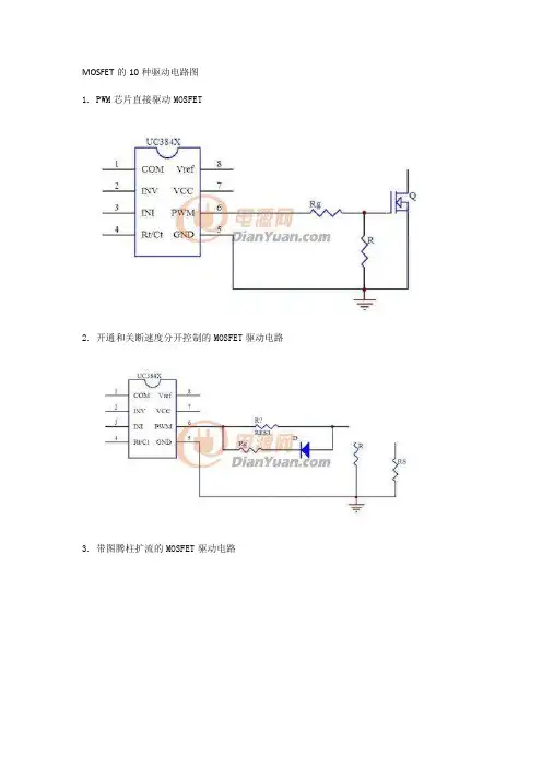
MOSFET的10种驱动电路图1. PWM芯片直接驱动MOSFET2. 开通和关断速度分开控制的MOSFET驱动电路3. 带图腾柱扩流的MOSFET驱动电路4. 使用TL494,SG3524内部的输出电路采用的单端集电极和射极开路的驱动电路5. 使用光耦隔离的驱动电路(原原理图有误,Q1\Q2位置对调)6. 使用光耦隔离的带负压关断驱动电路:(原原理图有误,Q1\Q2位置对调)7. 采用专用驱动光耦驱动的隔离驱动电路:8. 电动车控制器驱动电路9. P管驱动电路:10. 多管并联驱动电路:下面是赠送的几篇网络励志文章需要的便宜可以好好阅读下,不需要的朋友可以下载后编辑删除!!谢谢!!出路出路,走出去才有路“出路出路,走出去才有路。
”这是我妈常说的一句话,每当我面临困难及有畏难情绪的时候,我妈就用这句话来鼓励我。
一定有很多人想说:“这还在北京混个什么劲儿啊!”但他每天都乐呵呵的,就算把快递送错了也乐呵呵的。
某天,他突然递给我一堆其他公司的快递单跟我说:“我开了家快递公司,你看得上我就用我家的吧。
”我有点惊愕,有一种“哎呦喂,张老板好,今天还能三蹦子顺我吗”的感慨。
之后我却很少见他来,我以为是他孩子出生了休假去了。
再然后,我就只能见到单子见不到他了。
某天,我问起他们公司的快递员,小伙子说老板去上海了,在上海开了家新公司。
我很杞人忧天地问他:“那上海的市场不激烈吗?新快递怎么驻足啊!”小伙子嘿嘿一笑说:“我们老板肯定有办法呗!他都过去好几个月了,据说干得很不错呢!”“那老婆孩子呢?孩子不是刚生还很小吗?”“过去了,一起去上海了!”那个瞬间,我回头看了一眼办公室里坐着的各种愁眉苦脸的同事,并且举起手机黑屏幕照了一下我自己的脸,一股“人生已经如此的艰难,有些事情就不要拆穿”的气息冉冉升起。
并不是说都跳槽出去开公司才厉害,在公司瞪着眼睛看屏幕就是没发展,我是想说,只有勇气才能让自己作出改变。
我们每个人都觉得自己越活越内向,越来越自闭,越长大越孤单,以至于滋生了“换个新环境,我这种性格估计也不会跟其他人相处融洽,所以还是待着忍忍凑合过算了”的思想感情。

电力mosfet驱动电路特点电力MOSFET驱动电路是一种用于控制高功率MOSFET开关的电路,具有以下特点:1. 高速开关能力: 电力MOSFET驱动电路可以实现对MOSFET的快速开关,使其能够在毫秒甚至微秒的时间内完成快速开关动作。
这种高速开关能力使得电力MOSFET驱动电路在高频率开关电源、电机驱动等应用中得到广泛应用。
2. 低功耗: 电力MOSFET驱动电路采用了先进的功耗优化设计,能够在保证高性能的同时,尽量减小功耗。
这有助于提高系统的能效,减少能源消耗。
3. 高电压驱动能力: 电力MOSFET驱动电路能够提供足够的电流和电压来驱动MOSFET的栅极,保证其能够迅速切换。
这种高电压驱动能力使得电力MOSFET驱动电路适用于高电压应用场景,如电力电子装置。
4. 低输入电流: 电力MOSFET驱动电路的输入电流较低,可以通过外部逻辑电平或微控制器来控制。
这使得电力MOSFET驱动电路具有灵活性和可编程性,可以方便地集成到各种控制系统中。
5. 具有过温保护和短路保护功能: 电力MOSFET驱动电路通常具有过温保护和短路保护功能,当MOSFET温度过高或输出短路时,能够及时切断电源,以保护MOSFET和整个系统的安全运行。
6. 可靠性高: 电力MOSFET驱动电路采用了先进的保护电路和稳定的控制算法,能够有效地避免MOSFET的过压、过流等问题,提高系统的可靠性和稳定性。
7. 适应性强: 电力MOSFET驱动电路能够适应不同的电力MOSFET 器件,不同的工作条件和负载要求。
同时,电力MOSFET驱动电路还可以根据需求进行定制设计,以满足不同应用场景的需求。
总的来说,电力MOSFET驱动电路具有高速开关能力、低功耗、高电压驱动能力、低输入电流、过温保护和短路保护功能、高可靠性和适应性强等特点。
这些特点使得电力MOSFET驱动电路在各种高功率电子设备和系统中发挥着重要作用,提高了系统的性能和可靠性。

两种常见的MOSFET驱动电路设计常见的MOSFET驱动电路设计有两种:高侧驱动电路和低侧驱动电路。
高侧驱动电路是将MOSFET的源极连接到地,而负载连接到漏极。
这种电路设计的优点是可以在高侧实现PWM调光控制,因为调光信号是接在负载一侧,而不会影响到驱动信号。
高侧驱动电路的实现需要解决负载和电源之间的电位差问题。
一种常见的设计是使用一个电隔离器件,如光耦合器,它可以将输入信号隔离开,并提供一个离地的电位供电MOSFET。
另一种方法是使用一个NPN晶体管来驱动MOSFET,该晶体管的基极通过一个电阻连接到正电源,而发射极连接到MOSFET的源极,并且信号输入到晶体管的基极。
低侧驱动电路是将MOSFET的漏极连接到地,而负载连接到源极。
这种电路设计的优点是相对简单,不需要解决电位差的问题。
低侧驱动电路中最常见的设计时使用一个NPN晶体管将MOSFET的源极与地连接起来。
信号输入到NPN晶体管的基极,晶体管的发射极与MOSFET的源极相连。
当输入信号为高电平时,晶体管导通,MOSFET的源极与地之间产生一个低电平,从而导通MOSFET。
当输入信号为低电平时,晶体管截止,MOSFET被断开。
在设计这两种驱动电路时,需要考虑一些关键参数和特性,以确保MOSFET能够正常工作。
其中一个关键参数是驱动电压的选取。
驱动电压应该足够高以确保MOSFET能够完全导通,同时应该在MOSFET的最大耐压范围内。
另一个关键参数是驱动电流的选取。
驱动电流应该足够大以确保MOSFET能够迅速地从导通到截止的状态切换。
此外,还需要考虑电源的稳定性和电流能力。
为了防止驱动电路的电压波动对MOSFET的工作产生不利影响,应当使用稳定的电源。
此外,驱动电路还应能够提供足够的电流以确保MOSFET迅速地从导通到截止的状态切换。
综上所述,高侧驱动电路和低侧驱动电路是常见的MOSFET驱动电路设计。
通过正确选择驱动电压和驱动电流,并考虑电源稳定性和电流能力,可以确保MOSFET能够正常工作。

MOSFET管驱动电路的设计驱动电路的设计目标是提供足够的电压和电流给MOSFET的栅极,使其能够快速开关,并且保证可靠性和稳定性。
以下是一个典型的MOSFET驱动电路的设计步骤:1.选取适当的驱动电源:根据MOSFET的规格书,确定所需的驱动电压和电流。
选择一个能够提供足够电压和电流的电源。
2.添加驱动器:为了提供足够的电流给MOSFET的栅极,需要添加一个驱动器。
驱动器可以是单晶体管、场效应管或者运算放大器等。
选择适当的驱动器并配置合适的电阻和电容以确保稳定性。
驱动器应具有足够的增益和带宽以实现所需的开关速度。
3.添加隔离电路:为了避免MOSFET的开关特性对驱动器产生负面影响,需要在驱动器和MOSFET之间添加隔离电路。
隔离电路可以是光电耦合器、变压器等。
它们能够提供电气隔离并消除共模干扰。
4. 考虑反击电压:当MOSFET关闭时,由于电感元件的自感性,会产生一个反击电压。
该电压可能损坏驱动器和其他电路。
为了避免这种情况,可以添加一个反击二极管或者Zener二极管来保护电路。
5.添加保护电路:为了保护MOSFET不受过电压和过电流的损害,可以添加保护电路,如过压保护电路和过流保护电路。
这些保护电路可以使MOSFET在异常情况下自动关闭。
6.电路模拟和验证:设计完成后,通过电路模拟软件进行仿真验证以确保电路的性能和稳定性。
根据仿真结果调整电路参数直到满足设计要求。
7.PCB设计:根据电路设计结果进行PCB布局和布线。
要注意保持良好的地平面和电源平面,并分离驱动器和MOSFET的高电流回路和敏感信号线路。
8.测试和调试:制造和组装PCB后,进行测试和调试以验证电路的性能。
这包括检查驱动电源、驱动器输出和MOSFET的开关响应。
总之,MOSFET驱动电路的设计需要仔细考虑各种因素,包括驱动电源、驱动器的选择、隔离电路、反击电压和保护电路等。
通过合理的设计和仿真验证,可以实现可靠、稳定和高效的MOSFET驱动电路。

高速MOSFEMOSFET T栅极驱动电路的设计与应用指南摘要本文将展示一个用来设计高速开关应用所需的高性能栅极驱动电路的系统性方案。
它综合了各方面的信息,可一次性解决一些最常见的设计问题。
因此,各个层面的电力电子工程师都值得一读。
文中分析了一些最流行的电路方案及其性能,包括寄生元件、瞬间和极端工作条件的影响。
首先,文章对MOSFET技术和开关操作进行了大致讨论,从简单问题逐渐转向复杂问题,并详细讲述了低端和高端栅极驱动电路以及交流耦合和变压器隔离式方案的设计程序。
另外,文章还专门用一个章节的内容来讨论同步整流器应用中MOSFET的栅极驱动要求。
最后,本文还提供了多个分步骤的设计案例。
简介MOSFET,全称为金属氧化物半导体场效应晶体管,是电子产品领域各种高频高效开关应用的关键元器件。
FET技术发明于1930年,比双极晶体管还要早大约20年,这一点令人感到意外。
最早的信号级FET晶体管出现在20世纪50年代末,而功率MOSFET则是在70年代中期问世的。
如今,数百万的MOSFET 晶体管被集成到了各种电子元器件中,从微控制器到“离散式”功率晶体管。
本话题的重点在于各种开关模式电源转换应用中功率MOSFET的栅极驱动要求。
Design And Application GuideFor High Speed MOSFET Gate Drive CircuitsBy Laszlo BaloghABSTRACTThe main purpose of this paper is to demonstrate a systematic approach to design high performance gate drive circuits for high speed switching applications. It is an informative collection of topics offering a “one-stop-shopping” to solve the most common design challenges. Thus it should be of interest to power electronics engineers at all levels of experience.The most popular circuit solutions and their performance are analyzed, including the effect of parasitic components, transient and extreme operating conditions. The discussion builds from simple to more complex problems starting with an overview of MOSFET technology and switching operation. Design procedure for ground referenced and high side gate drive circuits, AC coupled and transformer isolated solutions are described in great details. A special chapter deals with the gate drive requirements of the MOSFETs in synchronous rectifier applications.Several, step-by-step numerical design examples complement the paper.INTRODUCTIONMOSFET – is an acronym for Metal Oxide Semiconductor Field Effect Transistor and it is the key component in high frequency, high efficiency switching applications across the electronics industry. It might be surprising, but FET technology was invented in 1930, some 20 years before the bipolar transistor. The first signal level FET transistors were built in the late 1950’s while power MOSFETs have been available from the mid 70’s. Today, millions of MOSFET transistors are integrated in modern electronic components, from microprocessors, through “discrete” power transistors.The focus of this topic is the gate drive requirements of the power MOSFET in various switch mode power conversion applications. MOSFET TECHNOLOGYThe bipolar and the MOSFET transistors exploit the same operating principle. Fundamentally, both type of transistors are charge controlled devices which means that their output current is proportional to the charge established in the semiconductor by the control electrode. When these devices are used as switches, both must be driven from a low impedance source capable of sourcing and sinking sufficient current to provide for fast insertion and extraction of the controlling charge. From this point of view, the MOSFETs have to be driven just as “hard” during turn-on and turn-off as a bipolar transistor to achieve comparable switching speeds. Theoretically, the switching speeds of the bipolar and MOSFET devices are close to identical, determined by the time required for the charge carriers to travel across the semiconductor region. Typical values in power devices are approximately 20 to 200 picoseconds depending on the size of the device. The popularity and proliferation of MOSFET technology for digital and power applications is driven by two of their major advantages over the bipolar junction transistors. One of these benefits is the ease of use of the MOSFET devices in high frequency switching applications. The MOSFET transistors are simpler to drive because their control electrode is isolated from the current conducting silicon, therefore a continuous ON current is not required. Once the MOSFET transistors are turned-on, their drive current is practically zero. Also, the controlling charge and accordingly the storage time in the MOSFET transistors is greatly reduced. This basically1eliminates the design trade-off between on state voltage drop – which is inversely proportional to excess control charge – and turn-off time. As a result, MOSFET technology promises to use much simpler and more efficient drive circuits with significant economic benefits compared to bipolar devices.Furthermore, it is important to highlight especially for power applications, that MOSFETs have a resistive nature. The voltage drop across the drain source terminals of a MOSFET is a linear function of the current flowing in the semiconductor. This linear relationship is characterized by the R DS(on) of the MOSFET and known as the on-resistance. On-resistance is constant for a given gate-to-source voltage and temperature of the device. As opposed to the -2.2mV/°C temperature coefficient of a p-n junction, the MOSFETs exhibit a positive temperature coefficient of approximately 0.7%/°C to 1%/°C. This positive temperature coefficient of the MOSFET makes it an ideal candidate for parallel operation in higher power applications where using a single device would not be practical or possible. Due to the positive TC of the channel resistance, parallel connected MOSFETs tend to share the current evenly among themselves. This current sharing works automatically in MOSFETs since the positive TC acts as a slow negative feedback system. The device carrying a higher current will heat up more – don’t forget that the drain to source voltages are equal – and the higher temperature will increase its R DS(on) value. The increasing resistance will cause the current to decrease, therefore the temperature to drop. Eventually, an equilibrium is reached where the parallel connected devices carry similar current levels. Initial tolerance in R DS(on) values and different junction to ambient thermal resistances can cause significant – up to 30% – error in current distribution.Device typesAlmost all manufacturers have got their unique twist on how to manufacture the best power MOSFETs, but all of these devices on the market can be categorized into three basic device types. These are illustrated in Figure 1.Figure 1. Power MOSFET device types Double-diffused MOS transistors were introduced in the 1970’s for power applications and evolved continuously during the years. Using polycrystalline silicon gate structures and self-aligning processes, higher density integration and rapid reduction in capacitances became possible. The next significant advancement was offered by the V-groove or trench technology to further increase cell density in power MOSFET devices. The better performance and denser integration don’t come free however, as trench MOS devices are more difficult to manufacture.The third device type to be mentioned here is the lateral power MOSFETs. This device type is constrained in voltage and current rating due to its inefficient utilization of the chip geometry. Nevertheless, they can provide significant benefits in low voltage applications, like in microprocessor power supplies or as synchronous rectifiers in isolated converters.2The lateral power MOSFETs have significantly lower capacitances, therefore they can switch much faster and they require much less gate drive power.MOSFET ModelsThere are numerous models available to illustrate how the MOSFET works, nevertheless finding the right representation might be difficult. Mostof the MOSFET manufacturers provide Spice and/or Saber models for their devices, but these models say very little about the application traps designers have to face in practice. They provide even fewer clues how to solve the most common design challenges.A really useful MOSFET model which would describe all important properties of the device from an application point of view would be very complicated. On the other hand, very simple and meaningful models can be derived of the MOSFET transistor if we limit the applicabilityof the model to certain problem areas.The first model in Figure 2 is based on the actual structure of the MOSFET device and can be used mainly for DC analysis. The MOSFET symbol in Figure 2a represents the channel resistance and the JFET corresponds to the resistance of the epitaxial layer. The length, thus the resistance of the epi layer is a function of the voltage rating of the device as high voltage MOSFETs require thicker epitaxial layer.Figure 2b can be used very effectively to model the dv/dt induced breakdown characteristic of a MOSFET. It shows both main breakdown mechanisms, namely the dv/dt induced turn-on of the parasitic bipolar transistor - present in all power MOSFETs - and the dv/dt induced turn-onof the channel as a function of the gate terminating impedance. Modern power MOSFETs are practically immune to dv/dt triggering of the parasitic npn transistor due to manufacturing improvements to reduce the resistance between the base and emitter regions.It must be mentioned also that the parasitic bipolar transistor plays another important role. Its base – collector junction is the famous body diode of the MOSFET.Figure 2. Power MOSFET models34Figure 2c is the switching model of the MOSFET. The most important parasitic components influencing switching performance are shown in this model. Their respective roles will be discussed in the next chapter which is dedicated to the switching procedure of the device.MOSFET Critical ParametersWhen switch mode operation of the MOSFET is considered, the goal is to switch between the lowest and highest resistance states of the device in the shortest possible time. Since the practical switching times of the MOSFETs (~10ns to 60ns) is at least two to three orders of magnitude longer than the theoretical switching time (~50ps to 200ps), it seems important to understand the discrepancy. Referring back to the MOSFET models in Figure 2, note that all models include three capacitors connected between the three terminals of the device. Ultimately, the switching performance of the MOSFET transistor is determined by how quickly the voltages can be changed across these capacitors.Therefore, in high speed switching applications, the most important parameters are the parasitic capacitances of the device. Two of these capacitors, the C GS and C GD capacitors correspond to the actual geometry of the device while the C DS capacitor is the capacitance of the base collector diode of the parasitic bipolar transistor (body diode).The C GS capacitor is formed by the overlap of the source and channel region by the gate electrode. Its value is defined by the actual geometry of the regions and stays constant (linear) under different operating conditions.The C GD capacitor is the result of two effects. Part of it is the overlap of the JFET region and the gate electrode in addition to the capacitance of the depletion region which is non-linear. The equivalent C GD capacitance is a function of the drain source voltage of the device approximated by the following formula:DS1GD,0GD V K 1C C ⋅+≈The C DS capacitor is also non-linear since it is the junction capacitance of the body diode. Its voltage dependence can be described as:DS 2DS,0DS V K C C ⋅≈Unfortunately, non of the above mentioned capacitance values are defined directly in the transistor data sheets. Their values are given indirectly by the C ISS , C RSS , and C OSS capacitor values and must be calculated as: RSSOSS DS RSS ISS GS RSSGD C C C C C C C C −=−== Further complication is caused by the C GD capacitor in switching applications because it is placed in the feedback path between the input and output of the device. Accordingly, its effective value in switching applications can be much larger depending on the drain source voltage of the MOSFET. This phenomenon is called the “Miller” effect and it can be expressed as:()GD L fs eqv GD,C R g 1C ⋅⋅+=Since the C GD and C DS capacitors are voltage dependent, the data sheet numbers are valid only at the test conditions listed. The relevant average capacitances for a certain application have to be calculated based on the required charge to establish the actual voltage change across the capacitors. For most power MOSFETs the following approximations can be useful: offDS,spec DS,spec OSS,ave OSS,off DS,spec DS,spec RSS,ave GD,V V C 2C V V C 2C ⋅⋅=⋅⋅=The next important parameter to mention is the gate mesh resistance, R G,I . This parasitic resistance describes the resistance associated by the gate signal distribution within the device. Its importance is very significant in high speed switching applications because it is in between the driver and the input capacitor of the device, directly impeding the switching times and the5dv/dt immunity of the MOSFET. This effect is recognized in the industry, where real high speed devices like RF MOSFET transistors use metal gate electrodes instead of the higher resistance polysilicon gate mesh for gate signal distribution. The R G,I resistance is not specified in the data sheets, but in certain applications it can be a very important characteristic of the device. In the back of this paper, Appendix A4 shows a typical measurement setup to determine the internal gate resistor value with an impedance bridge.Obviously, the gate threshold voltage is also a critical characteristic. It is important to note that the data sheet V TH value is defined at 25°C and at a very low current, typically at 250μA. Therefore, it is not equal to the Miller plateau region of the commonly known gate switching waveform. Another rarely mentioned fact about V TH is its approximately –7mV/°C temperature coefficient. It has particular significance in gate drive circuits designed for logic level MOSFET where V TH is already low under the usual test conditions. Since MOSFETs usually operate at elevated temperatures, proper gate drive design must account for the lower V TH when turn-off time, and dv/dt immunity is calculated as shown in Appendix A and F.The transconductance of the MOSFET is its small signal gain in the linear region of its operation. It is important to point out that every time the MOSFET is turned-on or turned-off, it must go through its linear operating mode where the current is determined by the gate-to-source voltage. The transconductance, g fs , is the small signal relationship between drain current and gate-to-source voltage:GSD fs dV dI g =Accordingly, the maximum current of the MOSFET in the linear region is given by: ()fs th GS D g V V I ⋅−=Rearranging this equation for V GS yields the approximate value of the Miller plateau as a function of the drain current.fs D th Miller GS,g IV V +=Other important parameters like the source inductance (L S ) and drain inductance (L D ) exhibit significant restrictions in switching performance. Typical L S and L D values are listed in the data sheets, and they are mainly dependant on the package type of the transistor. Their effects can be investigated together with the external parasitic components usually associated with layout and with accompanying external circuit elements like leakage inductance, a current sense resistor, etc.For completeness, the external series gate resistor and the MOSFET driver’s output impedance must be mentioned as determining factors in high performance gate drive designs as they have a profound effect on switching speeds and consequently on switching losses.SWITCHING APPLICATIONSNow, that all the players are identified, let’s investigate the actual switching behavior of the MOSFET transistors. To gain a better understanding of the fundamental procedure, the parasitic inductances of the circuit will be neglected. Later their respective effects on the basic operation will be analyzed individually. Furthermore, the following descriptions relate to clamped inductive switching because most MOSFET transistors and high speed gate drive circuits used in switch mode power supplies work in that operating mode.Figure 3. Simplified clamped inductive switchingmodelThe simplest model of clamped inductive switching is shown in Figure 3, where the DC current source represents the inductor. Its current can be considered constant during the short switching interval. The diode provides a path for the current during the off time of the MOSFET and clamps the drain terminal of the device to the output voltage symbolized by the battery.Turn-On procedureThe turn-on event of the MOSFET transistor can be divided into four intervals as depicted in Figure 4.Figure 4. MOSFET turn-on time intervalsIn the first step the input capacitance of the device is charged from 0V to V TH. During this interval most of the gate current is charging the C GS capacitor. A small current is flowing through the C GD capacitor too. As the voltage increases at the gate terminal and the C GD capacitor’s voltage has to be slightly reduced. This period is called the turn-on delay, because both the drain current and the drain voltage of the device remain unchanged.Once the gate is charged to the threshold level, the MOSFET is ready to carry current. In the second interval the gate is rising from V TH to the Miller plateau level, V GS,Miller. This is the linear operation of the device when current is proportional to the gate voltage. On the gate side, current is flowing into the C GS and C GD capacitors just like in the first time interval and the V GS voltage is increasing. On the output side of the device, the drain current is increasing, while the drain-to-source voltage stays at the previous level (V DS,OFF). This can be understood looking at the schematic in Figure 3. Until all the current is transferred into the MOSFET and the diode is turned-off completely to be able to block reverse voltage across its pn junction, the drain voltage must stay at the output voltage level. Entering into the third period of the turn-on procedure the gate is already charged to the sufficient voltage (V GS,Miller) to carry the entire load current and the rectifier diode is turned off. That now allows the drain voltage to fall. While the drain voltage falls across the device, the gate-to-source voltage stays steady. This is the Miller plateau region in the gate voltage waveform. All the gate current available from the driver is diverted to discharge the C GD capacitor to facilitate the rapid voltage change across the drain-to-source terminals. The drain current of the device stays constant since it is now limited by the external circuitry, i.e. the DC current source.The last step of the turn-on is to fully enhance the conducting channel of the MOSFET by applying a higher gate drive voltage. The final amplitude of V GS determines the ultimate on-resistance of the device during its on-time. Therefore, in this fourth interval, V GS is increased from V GS,Miller to its final value, V DRV. This is accomplished by charging the C GS and C GD capacitors, thus gate current is now split between the two components. While these capacitors are being charged, the drain current is still constant, and the drain-to-source voltage is slightly decreasing as the on-resistance of the device is being reduced.6Turn-Off procedureThe description of the turn-off procedure for the MOSFET transistor is basically back tracking the turn-on steps from the previous section. Start with V GS being equal to V DRV and the current in the device is the full load current represented by I DC in Figure 3. The drain-to-source voltage is being defined by I DC and the R DS(on) of the MOSFET. The four turn-off steps are shown in Figure 5. for completeness.Figure 5. MOSFET turn-off time intervals The first time interval is the turn-off delay which is required to discharge the C ISS capacitance from its initial value to the Miller plateau level. During this time the gate current is supplied by the C ISS capacitor itself and it is flowing through the C GS and C GD capacitors of the MOSFET. The drain voltage of the device is slightly increasing as the overdrive voltage is diminishing. The current in the drain is unchanged.In the second period, the drain-to-source voltage of the MOSFET rises from I D⋅R DS(on) to the final V DS(off) level, where it is clamped to the output voltage by the rectifier diode according to the simplified schematic of Figure 3. During this time period – which corresponds to the Miller plateau in the gate voltage waveform - the gate current is strictly the charging current of the C GDcapacitor because the gate-to-source voltage is constant. This current is provided by the bypass capacitor of the power stage and it is subtracted from the drain current. The total drain current still equals the load current, i.e. the inductor current represented by the DC current source in Figure 3.The beginning of the third time interval is signified by the turn-on of the diode, thus providing an alternative route to the load current.The gate voltage resumes falling from V GS,Miller to V TH. The majority of the gate current is coming out of the C GS capacitor, because the C GDcapacitor is virtually fully charged from the previous time interval. The MOSFET is in linear operation and the declining gate-to-source voltage causes the drain current to decrease and reach near zero by the end of this interval.Meanwhile the drain voltage is steady at V DS(off)due to the forward biased rectifier diode.The last step of the turn-off procedure is to fully discharge the input capacitors of the device. V GSis further reduced until it reaches 0V. The bigger portion of the gate current, similarly to the third turn-off time interval, supplied by the C GScapacitor. The drain current and the drain voltage in the device are unchanged.Summarizing the results, it can be concluded that the MOSFET transistor can be switched between its highest and lowest impedance states (either turn-on or turn-off) in four time intervals. The lengths of all four time intervals are a function of the parasitic capacitance values, the required voltage change across them and the available gate drive current. This emphasizes the importance of the proper component selection and optimum gate drive design for high speed, high frequency switching applications.7Characteristic numbers for turn-on, turn-off delays, rise and fall times of the MOSFET switching waveforms are listed in the transistor data sheets. Unfortunately, these numbers correspond to the specific test conditions and to resistive load, making the comparison of different manufacturers’ products difficult. Also, switching performance in practical applications with clamped inductive load is significantly different from the numbers given in the data sheets.Power lossesThe switching action in the MOSFET transistorin power applications will result in some unavoidable losses, which can be divided into two categories.The simpler of the two loss mechanisms is the gate drive loss of the device. As described before, turning-on or off the MOSFET involves chargingor discharging the C ISS capacitor. When the voltage across a capacitor is changing, a certain amount of charge has to be transferred. The amount of charge required to change the gate voltage between 0V and the actual gate drive voltage V DRV, is characterized by the typical gate charge vs. gate-to-source voltage curve in the MOSFET datasheet. An example is shown in Figure 6.Figure 6. Typical gate charge vs. gate-to-sourcevoltage This graph gives a relatively accurate worst case estimate of the gate charge as a function of the gate drive voltage. The parameter used to generate the individual curves is the drain-to-source off state voltage of the device. V DS(off) influences the Miller charge – the area below the flat portion of the curves – thus also, the total gate charge required in a switching cycle. Once the total gate charge is obtained from Figure 6, the gate charge losses can be calculated as:DRVGDRVGATEfQVP⋅⋅=where V DRV is the amplitude of the gate drive waveform and f DRV is the gate drive frequency – which is in most cases equal to the switching frequency. It is interesting to notice that the Q G⋅f DRV term in the previous equation gives the average bias current required to drive the gate. The power lost to drive the gate of the MOSFET transistor is dissipated in the gate drive circuitry. Referring back to Figures 4 and 5, the dissipating components can be identified as the combination of the series ohmic impedances in the gate drive path. In every switching cycle the required gate charge has to pass through the driver output impedances, the external gate resistor, and the internal gate mesh resistance. As it turns out, the power dissipation is independent of how quickly the charge is delivered through the resistors. Using the resistor designators from Figures 4 and 5, the driver power dissipation can be expressed as:OFFDRV,ONDRV,DRVIG,GATELODRVGDRVLOOFFDRV,IG,GATEHIDRVGDRVHIONDRV,PPPRRRfQVR21PRRRfQVR21P+=++⋅⋅⋅⋅=++⋅⋅⋅⋅=In the above equations, the gate drive circuit is represented by a resistive output impedance and this assumption is valid for MOS based gate drivers. When bipolar transistors are utilized in the gate drive circuit, the output impedance becomes non-linear and the equations do not yield the correct answers. It is safe to assume that with low value gate resistors (<5Ω) most gate drive losses are dissipated in the driver. If R GATE is sufficiently large to limit I G below the output89current capability of the bipolar driver, the majority of the gate drive power loss is then dissipated in R GATE .In addition to the gate drive power loss, the transistors accrue switching losses in the traditional sense due to high current and high voltage being present in the device simultaneously for a short period. In order to ensure the least amount of switching losses, the duration of this time interval must be minimized. Looking at the turn-on and turn-off procedures of the MOSFET, this condition is limited to intervals 2 and 3 of the switching transitions in both turn-on and turn-off operation. These time intervals correspond to the linear operation of the device when the gate voltage is between V TH and V GS,Miller , causing changes in the current of the device and to the Miller plateau region when the drain voltage goes through its switching transition.This is a very important realization to properly design high speed gate drive circuits. It highlights the fact that the most important characteristic of the gate driver is its source-sink current capability around the Miller plateau voltage level. Peak current capability, which is measured at full V DRV across the driver’s output impedance, has very little relevance to the actual switching performance of the MOSFET. What really determines the switching times of the device is the gate drive current capability when the gate-to-source voltage, i.e. the output of the driver is at ~5V (~2.5V for logic level MOSFETs).A crude estimate of the MOSFET switching losses can be calculated using simplified linear approximations of the gate drive current, drain current and drain voltage waveforms during periods 2 and 3 of the switching transitions. First the gate drive currents must be determined for the second and third time intervals respectively:()G.I GATE HI MillerGS,DRV G3G.IGATE HI TH Miller GS,DRVG2R R R V V I R R R V V 0.5V I ++−=+++⋅−=Assuming that I G2 charges the input capacitor of the device from V TH to V GS,Miller and I G3 is the discharge current of the C RSS capacitor while the drain voltage changes from V DS(off) to 0V, the approximate switching times are given as:G3offDS,RSS G2THMillerGS,ISS I V C t3I V V C t2⋅=−⋅=During t2 the drain voltage is V DS(off) and the current is ramping from 0A to the load current, I L while in t3 time interval the drain voltage is falling from V DS(off) to near 0V. Again, using linear approximations of the waveforms, the power loss components for the respective time intervals can be estimated:Loff DS,Loff DS,I 2V T t3P32I V T t2P2⋅⋅=⋅⋅=where T is the switching period. The total switching loss is the sum of the two loss components, which yields the following simplifed expression:Even though the switching transitions are well understood, calculating the exact switching losses is almost impossible. The reason is the effect of the parasitic inductive components which will significantly alter the current and voltage waveforms, as well as the switching times during the switching procedures. Taking into account the effect of the different source and drain inductances of a real circuit would result in second order differential equations to describe the actual waveforms of the circuit. Since the variables, including gate threshold voltage, MOSFET capacitor values, driver output impedances, etc. have a very wide tolerance, the above described linear approximation seems to be a reasonable enough compromise to estimate switching losses in the MOSFET.Effects of parasitic componentsThe most profound effect on switching performance is exhibited by the source inductance. There are two sources for parasitic source inductance in a typical circuit, the sourceTt3t22I V P L DS(off)SW +⋅⋅=。

MOSFET驱动电路设计参考MOSFET(金属氧化物半导体场效应晶体管)驱动电路是控制MOSFET开关的电路,它提供适当的电流和电压来确保MOSFET能够在正确的时间和条件下完全关闭和打开。
MOSFET驱动电路设计需要考虑到反馈和保护机制、功耗和效率以及电流和电压需求等因素。
以下是一些MOSFET驱动电路设计的参考。
1.电流放大器驱动电路:电流放大器是一种被广泛使用的MOSFET驱动电路设计,它通过升压变压器和反馈电路来将电流放大,并且能够提供足够的电流来驱动MOSFET。
这种电路设计具有简单、可靠和成本低廉的特点。
2.隔离式驱动电路:隔离式驱动电路是一种通过电流隔离器将控制电路与MOSFET隔离开来的设计。
通过隔离电路,可以阻止外部电路中的噪声、干扰和电压峰值对MOSFET的影响。
这种驱动电路设计适用于需要高耐受性和抗干扰性的应用。
3.模拟驱动电路:模拟驱动电路利用可变电流源来控制MOSFET。
这种设计需要一个与控制信号相对应的电压源,以确保MOSFET的开启和关闭速度与输入信号相匹配。
模拟驱动电路适用于需要快速响应和高精确度的应用,如音频放大器和直流直流变换器。
4.逻辑驱动电路:逻辑驱动电路是一种基于逻辑门电路的设计,通过逻辑门来控制MOSFET的开关。
逻辑驱动电路具有简单、易实现和低功耗的特点,适用于数字电路中的应用。
在设计MOSFET驱动电路时,还需要考虑以下几个关键因素:1.电流和电压需求:根据MOSFET的规格和应用需求,确保设计的驱动电路能够提供足够的电流和电压来使MOSFET达到预期的工作状态。
2.反馈和保护机制:添加适当的反馈和保护电路,如电流限制器和短路保护器,以确保MOSFET在超载、短路或其他异常情况下得到保护。
3.功耗和效率:通过优化电路设计和选择高效的元件来降低功耗,提高效率。
例如,可以选择低电阻的电源和高效的驱动器。
4.温度控制和散热设计:合理布局电路和选择散热器,以降低MOSFET的工作温度,提高可靠性和稳定性。
高速MOSFET门极驱动电路的设计应用指南一、背景介绍二、设计步骤及要点1.确定MOSFET型号和工作条件:根据实际应用需求,选择合适的MOSFET型号,并确定其工作电压和电流。
这些参数将直接影响到驱动电路的设计。
2.确定驱动电源电压和电流:根据MOSFET的特性参数,选择合适的驱动电源电压和电流。
一般来说,高速应用中通常需要较高的电源电压和电流,以确保MOSFET能够迅速开关。
3.选择驱动芯片或设计驱动电路:根据以上参数,选择合适的驱动芯片或自行设计驱动电路。
常用的驱动芯片有IR2110、TC4420等,可以根据实际应用需求选择合适的芯片。
4.进行驱动电路的布局和连接:根据驱动芯片或电路设计,进行布局和连接。
注意保持短而稳定的门极连接线路,尽量减小电流环路和电磁干扰。
5.添加保护电路:考虑MOSFET的过电流、过压等保护问题,设计相应的保护电路,以确保MOSFET的安全工作。
6.进行仿真和测试:通过仿真软件进行仿真分析,验证电路设计是否满足要求。
同时,进行实际测试,检查电路的性能和稳定性。
三、高速MOSFET门极驱动电路的典型设计示例下图为一种常用的高速MOSFET门极驱动电路设计示例,以IR2110为例:[电路图]该驱动电路可实现高速的MOSFET开关控制,具有较高的转换效率和可靠性。
其中VCC为驱动电源电压,VDD为MOSFET的工作电源电压,VIN为控制信号输入端,VD为MOSFET的漏极电压,R1和R2为限流电阻,D1为反向恢复二极管。
四、设计注意事项1.选择合适的驱动芯片或自行设计驱动电路时,要充分考虑芯片的最大驱动电流和工作频率等参数,以确保其满足实际应用需求。
2.在设计驱动电路时,要注意尽量减小电流回路和电磁干扰,保持稳定的门极连接线路。
3.添加合适的保护电路,以保护MOSFET免受过电流、过压等故障的影响。
4.在设计完成后,进行仿真分析和实际测试,检查电路的性能和稳定性,并及时进行调整和改进。
两种常见的MOSFET驱动电路设计MOSFET驱动电路是一种常见的电路设计,用于控制和驱动MOSFET晶体管的工作。
MOSFET驱动电路的设计能够确保MOSFET的开关速度,其选择和设计影响到整个电路的性能和可靠性。
以下是两种常见的MOSFET驱动电路设计。
1.单级放大器驱动电路单级放大器驱动电路是一种简单而常见的MOSFET驱动电路设计。
它包含一个放大器和一个偏置电源电路。
其输入端连接到信号源,输出端连接到MOSFET的门极。
当输入信号施加到放大器时,放大器将信号放大至足够高的电压,以控制MOSFET的开关。
单级放大器驱动电路的优点是简单,易于设计和实现。
然而,它可能存在驱动能力不足的问题。
因此,在应用中通常需要考虑额外的电流放大器或放大器级联来增加驱动能力。
2.高侧驱动电路高侧驱动电路是另一种常见的MOSFET驱动电路设计。
高侧驱动电路用于控制高侧(负载连接在电源正极的一侧)MOSFET。
它需要一个额外的电源电路和驱动电路来实现。
高侧驱动电路通常包含一个电源电路,用于提供MOSFET的驱动电压。
该电源电路可以是一个开关电源或线性调节电源。
驱动电路通常由电流源、驱动变压器和栅极驱动电路组成。
电流源用于提供驱动电路所需的电流,驱动变压器用于隔离输入信号源和MOSFET,以减小信号干扰和保护信号源。
高侧驱动电路的优点是能够驱动高侧MOSFET,使其能够正常工作。
然而,高侧驱动电路的设计复杂,需要考虑保护电路和故障检测电路,以确保其可靠性和安全性。
除了以上两种常见的MOSFET驱动电路设计,还有其他一些特殊应用的驱动电路,例如三相桥式驱动电路、半桥和全桥驱动电路等。
这些电路设计根据具体应用需求和性能要求可能有所不同,但基本的驱动原理和设计方法是相似的。
总之,MOSFET驱动电路设计是一项重要而复杂的工作,旨在保证MOSFET工作的可靠性和性能。
根据具体的应用需求和性能要求,选择合适的驱动电路设计,并考虑保护措施和故障检测电路,以确保电路的可靠性和安全性。
高速MOS驱动电路设计和应用指南摘要本篇论文的主要目的是来论证一种为高速开关应用而设计高性能栅极驱动电路的系统研究方法。
它是对“一站买齐”主题信息的收集,用来解决设计中最常见的挑战。
因此,各级的电力电子工程师对它都应该感兴趣。
对最流行电路解决方案和他们的性能进行了分析,这包括寄生部分的影响、瞬态的和极限的工作情况。
整篇文章开始于对MOSFET技术和开关工作的概述,随后进行简单的讨论然后再到复杂问题的分析。
仔细描述了设计过程中关于接地和高边栅极驱动电路、AC耦合和变压器隔离的解决方案。
其中一个章节专门来解决同步整流器应用中栅极驱动对MOSFET的要求。
另外,文章中还有一些一步一步的参数分析设计实例。
简介MOSFET是Metal Oxide Semiconductor Field Effect Transistor的首字母缩写,它在电子工业高频、高效率开关应用中是一种重要的元件。
或许人们会感到不可思议,但是FET是在1930年,大约比双极晶体管早20年被发明出来。
第一个信号电平FET晶体管制成于二十世纪60年代末期,而功率MOSFET是在二十世纪80年代开始被运用的。
如今,成千上万的MOSFET晶体管集成在现代电子元件,从微型的到“离散”功率晶体管。
本课题的研究重点是在各种开关模型功率转换应用中栅极驱动对功率MOSFET 的要求。
场效应晶体管技术双极晶体管和场效应晶体管有着相同的工作原理。
从根本上说,,两种类型晶体管均是电荷控制元件,即它们的输出电流和控制极半导体内的电荷量成比例。
当这些器件被用作开关时,两者必须和低阻抗源极的拉电流和灌电流分开,用以为控制极电荷提供快速的注入和释放。
从这点看,MOS-FET在不断的开关,当速度可以和双极晶体管相比拟时,它被驱动的将十分的‘激烈’。
理论上讲,双极晶体管和MOSFET的开关速度是基本相同的,这取决与载流子穿过半导体所需的时间。
在功率器件的典型值为20 ~ 200皮秒,但这个时间和器件的尺寸大小有关。
一种基于光耦HCPL0601的光电隔离型功率MOSFET驱动电路近年来,随着计算机、通信、家电等电子设备的不断发展,对高速、高性能、高可靠度电路的需求逐渐增加。
而光电隔离型功率MOSFET驱动电路因其具有的大功率、长寿命、耐高温的特点,已成为目前应用广泛的电路设计之一。
其中,光耦HCPL0601作为一种典型的光电耦合器,在光电隔离型功率MOSFET驱动电路中具有重要的作用。
光电隔离型功率MOSFET驱动电路由光电耦合器、MOSFET 驱动电路、直流电源和控制信号输入端等组成。
光耦HCPL0601是该电路中的核心元件,其内部集成了红外发光二极管和光敏二极管,可以实现光信号和电信号的隔离。
而功率MOSFET则是驱动电路的基本元件,可以实现高速信号的放大和控制。
在光电隔离型功率MOSFET驱动电路中,光耦HCPL0601发出的光信号被光敏二极管接收,并被转化为电信号输入到MOSFET驱动电路中。
MOSFET驱动电路对输入信号进行放大和处理,并输出控制信号控制功率MOSFET的通断。
通过这种方式,可以实现对电路中的负载进行控制,从而实现电路的正常工作。
光电隔离型功率MOSFET驱动电路具有以下优点:首先,由于光电耦合器实现信号的隔离,因此可以大大降低电路受到干扰的风险,提高电路的抗干扰能力和可靠性。
其次,由于光电耦合器的寿命很长,因此这种电路还具有高稳定性和长寿命的优点。
另外,功率MOSFET的响应速度快,可以实现高速控制,适用于许多高速电路设计。
总之,基于光耦HCPL0601的光电隔离型功率MOSFET驱动电路具有重要的应用价值,适用于许多电路设计。
在电子设备的设计过程中,需要根据实际情况选择合适的元器件和电路方案,以实现更高效、更稳定、更可靠的电路设计。