IC datasheet pdf-CD74ACT240,PDF(CD54_74AC240_241_244, CD54_74ACT240_241_244)
- 格式:pdf
- 大小:1.11 MB
- 文档页数:16

74VHC240OCTAL BUS BUFFERWITH 3STATE OUTPUTS (INVERTED)June 1999s HIGH SPEED:t PD =3.6ns (TYP.)at V CC =5V sLOW POWER DISSIPATION:I CC =4µA (MAX.)at T A =25o C sHIGH NOISE IMMUNITY:V NIH =V NIL =28%V CC (MIN.)s POWER DOWN PROTECTION ON INPUTS sSYMMETRICAL OUTPUT IMPEDANCE:|I OH |=I OL =8mA (MIN)sBALANCED PROPAGATION DELAYS:t PLH ≅t PHLsOPERATING VOLTAGERANGE:V CC (OPR)=2V to 5.5VsPIN AND FUNCTION COMPATIBLE WITH 74SERIES 240s IMPROVED LATCH-UP IMMUNITY sLOW NOISE:V OLP =0.9V(Max.)DESCRIPTIONThe 74VHC240is an advanced high-speed CMOS OCTAL BUS BUFFER (3-STATE)fabricated with sub-micron silicon gate and double-layer metal wiring C 2MOS technology.G output enable governs four BUS BUFFERs.This device is designed to be used with 3state memory address drivers,etc.Power down protection is provided on all inputs and 0to 7V can be accepted on inputs with no regard to the supply voltage.This device can be used to interface 5V to 3V.All inputs and outputs are equipped with protection circuits against static discharge,giving them 2KV ESD immunity and transient excess voltage.PIN CONNECTION AND IEC LOGIC SYMBOLSORDER CODES :74VHC240M 74VHC240TM(Micro Package)T(TSSOP Package)®1/8TRUTH TABLEINPUTOUTPUTG An Yn L L H L H L HXZX:”H”or ”L”Z:High impe dancePIN DESCRIPTIONPIN NoSYMBOLNAME AND FUNCTION 11G Output Enable Input 2,4,6,81A1to 1A4Data Inputs 9,7,5,32Y1to 2Y4Data Outputs 11,13,15,172A1to 2A4Data Inputs 18,16,14,121Y1to 1Y4Data Outputs 192G Output Enable Input 10GND Ground (0V)20V CCPositive Supply VoltageABSOLUTE MAXIMUM RATINGSSymbol ParameterValue Unit V CC Supply Voltage -0.5to +7.0V V I DC Input Voltage -0.5to +7.0V V O DC Output Voltage -0.5to V CC +0.5V I IK DC Input Diode Current -20mA I OK DC Output Diode Current ±20mA I O DC Output Current ±25mA I CC orI GN DDC V CC or Ground Current ±75mAT stg Storage Temperature -65to +150o C T LLead Temperature (10sec)300oCAbsolute Maximum Ratingsarethose values beyond which dam age to the device may occur.Functional operation un der these condition is not implied.RECOMMENDED OPERATING CONDITIONSSymbol ParameterValue Unit V CC Supply Voltage 2.0to 5.5V V I Input Voltage 0to 5.5V V O Output Voltage 0to V CC VT op Operating Temperature-40to+85oCdt/dvInput Rise and Fall Time (see note 1)(V CC =3.3±0.3V)(V CC =5.0±0.5V)0to 1000to 20ns/V ns/V1)V IN from 30%to70%of V CCINPUT EQUIVALENT CIRCUIT74VHC2402/8AC ELECTRICAL CHARACTERISTICS (Input t r =t f =3ns)SymbolParameterTest Condition ValueUnitV CC (V)C L (pF)T A =25oC-40to 85oCMin.Typ.Max.Min.Max.t PLH t PHL Propagation Delay Time3.3(*)15 5.37.5 1.09.0ns3.3(*)507.811.0 1.012.55.0(**)15 3.6 5.5 1.0 6.55.0(**)50 5.17.51.08.5t PZL t PZHOutput Enable Time3.3(*)15R L =1K Ω 6.610.6 1.012.5ns3.3(*)50R L =1K Ω9.114.1 1.016.05.0(**)15R L =1K Ω 4.77.3 1.08.55.0(**)50R L =1K Ω6.29.3 1.010.5t PL Z t PH Z Output Disable Time 3.3(*)50R L =1K Ω10.314.0 1.016.0ns 5.0(**)50R L =1K Ω6.79.2 1.010.5t OSLH t OSHLOutput to Output Skew Time (note 1)3.3(*)50 1.5 1.5ns5.0(**)501.01.0(*)Voltag e range is 3.3V ±0.3V (**)Voltage range is 5V ±0.5VNote 1:Parameter guaranteed bydesign.t soLH =|t pLHm -t pLHn |,t soHL =|t pHLm -t pHLn |DC SPECIFICATIONSSymbolParameterTest Conditions ValueUnitV CC (V)T A =25oC -40to 85oC Min.Typ.Max.Min.Max.V IH High Level Input Voltage 2.0 1.5 1.5V 3.0to 5.50.7V CC0.7V CCV IL Low Level Input Voltage2.00.50.5V3.0to 5.50.3V CC0.3V CC V OHHigh Level Output Voltage2.0I O =-50µA 1.9 2.0 1.9V3.0I O =-50µA 2.9 3.0 2.94.5I O =-50µA 4.4 4.54.43.0I O =-4mA 2.58 2.484.5I O =-8mA 3.943.8V OLLow Level Output Voltage2.0I O =50µA 0.00.10.1V3.0I O =50µA 0.00.10.14.5I O =50µA 0.00.10.13.0I O =4mA 0.360.444.5I O =8mA 0.360.44I OZHigh Impedance Output Leakage Current5.5V I =V IH orV IL V O =V CC orGND ±0.25±2.5µAI I Input Leakage Current 0to 5.5V I =5.5V or GND ±0.1±1.0µA I CCQuiescent Supply Current5.5V I =V CC orGND440µA74VHC2403/8CAPACITIVE CHARACTERISTICSSymbolParameterTest ConditionsValueUnitT A =25oC -40to 85oC Min.Typ.Max.Min.Max.C IN Input Capacitance 41010pF C OUT Output Capacitance 6pF C PDPower Dissipation Capacitance (note 1)17pF1)C PD isdefined as the value of the IC’sinternal equiva lent capacitance which is calculated fromthe operating current consumption without load.(Referto Test Circuit).Average operating current can be obtained bythe following equation.I CC (opr)=C PD •V CC •f IN +I CC /8(per Circuit)TEST CIRCUITTESTSWITCH t PLH ,t PHL Open t PZL ,t PLZ V CC t PZH ,t PHZGNDC L =15/50pF or equ ivalent (includes jigand probe capacitance)R L =R 1=1K ΩorequivalentR T =Z OU T of pulse generator (typ ically 50Ω)DYNAMIC SWITCHING CHARACTERISTICSSymbolParameterTest Conditions ValueUnitV CC (V)T A =25oC -40to 85oC Min.Typ.Max.Min.Max.V OLP Dynamic Low Voltage Quiet Output (note 1,2) 5.0C L =50pF0.60.9VV OLV -0.9-0.6V IHD Dynamic High Voltage Input (note 1,3) 5.0 3.5V ILDDynamic Low Voltage Input (note 1,3)5.01.51)Worst case package.2)Max num ber of outputs defined as (n).Data inputs aredriven 0V to 5.0V,(n -1)outputs switching and one out put at GND.3)Max num ber of data inputs (n)switching.(n-1)switching 0V to5.0V.Inputs under test switching:5.0V to threshold (V ILD ),0V to threshold (V IHD ),f=1MHz.74VHC2404/874VHC240 WAVEFORM1:PROPAGATION DELAYS(f=1MHz;50%duty cycle)WAVEFORM2:OUTPUT ENABLE AND DISABLE TIME(f=1MHz;50%duty cycle)5/8DIM.mm inch MIN.TYP.MAX.MIN.TYP.MAX.A 2.650.104a10.100.200.0040.007a2 2.450.096b 0.350.490.0130.019b10.230.320.0090.012C 0.500.020c145(typ.)D 12.6013.000.4960.512E 10.0010.650.3930.419e 1.270.050e311.430.450F 7.407.600.2910.299L 0.50 1.270.190.050M 0.750.029S8(max.)P013LSO-20MECHANICAL DATA74VHC2406/8DIM.mminch MIN.TYP.MAX.MIN.TYP.MAX.A 1.10.433A10.050.100.150.0020.0040.006A20.850.90.950.3350.3540.374b 0.190.300.00750.0118c 0.090.20.00350.0079D 6.4 6.5 6.60.2520.2560.260E 6.25 6.4 6.50.2460.2520.256E1 4.34.4 4.480.1690.1730.176e 0.65BSC0.0256BSCK 0o 4o 8o 0o 4o 8o L0.500.600.700.0200.0240.028cEbA2AE1D1PIN 1IDENTIFICATIONA1LK eTSSOP20MECHANICAL DATA74VHC2407/874VHC240Information furnished is believed to be accurate and reliable.However,STMicroelectronics assumes no responsibility for the consequence s of use of such information nor for any infringement of patents or other rights of third parties which may result from its use.No license is granted by implication or otherwise under any patent or patent rights of STMicroelectronics.Specification mentioned in this publication are subject to change without notice.This publication supersedes and replaces all information previously supplied.STMicroelectronics products are not authorized for use as critical components in life support devices or systems without express written approval of STMicroelectronics.The ST logo is a trademark of STMicroelectronics©1999STMicroelectronics–Printed in Italy–All Rights ReservedSTMicroelectronics GROUP OF COMPANIESAustralia-Brazil-Canada-China-France-Germany-Italy-Japan-Korea-Malaysia-Malta-Mexico-Morocco-The Netherlands-Singapore-Spain-Sweden-Switzerland-Taiwan-Thailand-United Kingdom-U.S.A..8/8。
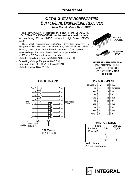
O CTAL 3-S TATE N ONINVERTINGB UFFER/L INE D RIVER/L INE R ECEIVERHigh-Speed Silicon-Gate CMOS The IN74ACT244 is identical in pinout to the LS/ALS244, HC/HCT244. The IN74ACT244 may be used as a level converterfor interfacing TTL or NMOS outputs to High Speed CMOSinputs.designed to be used with 3-state memory address drivers, clocknoninverting outputs and two active-low output enables.•TTL/NMOS Compatible Input Levels•Outputs Directly Interface to CMOS, NMOS, and TTL•Operating Voltage Range: 4.5 to 5.5 V •Low Input Current: 1.0 µA; 0.1 µA @ 25°C •Outputs Source/Sink 24 mAORDERING INFORMATIONIN74ACT244N PlasticIN74ACT244DW SOICT A = -40° to 85° C for allpackagesFUNCTION TABLEInputs Outputs Enable A,Enable BA,B YA,YBL L LL H HH X ZX=don’t careZ = high impedanceLOGIC DIAGRAMPIN 20=V CCPIN 10 = GNDPIN ASSIGNMENTMAXIMUM RATINGS*Symbol Parameter ValueUnit V CC DC Supply Voltage (Referenced to GND) -0.5 to +7.0 VV IN DC Input Voltage (Referenced to GND) -0.5 to V CC +0.5 VV OUT DC Output Voltage (Referenced to GND) -0.5 to V CC +0.5 VI IN DC Input Current, per Pin ±20 mAI OUT DC Output Sink/Source Current, per Pin ±50 mAI CC DC Supply Current, V CC and GND Pins ±50 mAP D Power Dissipation in Still Air, Plastic DIP+ SOIC Package+ 750500mWTstg Storage Temperature -65 to +150 °CT L Lead Temperature, 1 mm from Case for 10Seconds(Plastic DIP or SOIC Package)260 °C*Maximum Ratings are those values beyond which damage to the device may occur.Functional operation should be restricted to the Recommended Operating Conditions.+Derating - Plastic DIP: - 10 mW/°C from 65° to 125°CSOIC Package: - 7 mW/°C from 65° to 125°CRECOMMENDED OPERATING CONDITIONSSymbol Parameter MinMaxUnit V CC DC Supply Voltage (Referenced to GND) 4.5 5.5 VV IN, V OUT DC Input Voltage, Output Voltage (Referenced toGND)0 V CC VT J Junction Temperature (PDIP) 140 °CT A Operating Temperature, All Package Types -40 +85 °CI OH Output Current - High -24 mAI OL Output Current - Low 24 mAt r, t f Input Rise and Fall Time * (except Schmitt Inputs) V CC=4.5 VV CC =5.5 V108.0ns/V* VINfrom 0.8 V to 2.0 VThis device contains protection circuitry to guard against damage due to high static voltages or electric fields. However, precautions must be taken to avoid applications of any voltage higher than maximum rated voltages to this high-impedance circuit. For proper operation, V IN and V OUT should be constrained to the range GND≤(V IN or V OUT)≤V CC.Unused inputs must always be tied to an appropriate logic voltage level (e.g., either GND or V CC). Unused outputs must be left open.DC ELECTRICAL CHARACTERISTICS (Voltages Referenced to GND)V CC Guaranteed LimitsSymbol Parameter Test Conditions V 25 °C -40°C to85°CUnit V IH Minimum High-Level Input VoltageV OUT = V CC -0.1 V 4.5 5.5 2.0 2.0 2.0 2.0 VV IL Maximum Low -Level Input VoltageV OUT =0.1 V 4.5 5.5 0.8 0.8 0.8 0.8 VV OH Minimum High-Level Output VoltageI OUT ≤ -50 µA 4.5 5.5 4.4 5.4 4.4 5.4 V*V IN =V IHI OH =-24 mAI OH =-24 mA4.55.5 3.86 4.86 3.76 4.76 V OL Maximum Low-Level Output VoltageI OUT ≤ 50 µA 4.5 5.5 0.1 0.1 0.1 0.1 V*V IN =V ILI OL =24 mAI OL =24 mA4.55.5 0.36 0.36 0.44 0.44 I IN Maximum Input Leakage CurrentV IN =V CC or GND 5.5 ±0.1 ±1.0 µAI OZ Maximum Three-State Leakage Current V IN (OE)=V IL or V IH V IN =V CC or GND V OUT =V CC or GND5.5 ±0.5 ±5.0 µA∆I CCT Additional MaxI CC /InputV IN =V CC - 2.1 V 5.5 1.5 mA I OLD +Minimum Dynamic Output CurrentV OLD =1.65 V Max 5.5 75 mAI OHD +Minimum Dynamic Output CurrentV OHD =3.85 V Min 5.5 -75 mAI CC Maximum Quiescent Supply Current(per Package)V IN =V CC or GND 5.5 8.0 80 µAAll outputs loaded; thresholds on input associated with output under test. +Maximum test duration 2.0 ms, one output loaded at a time.AC ELECTRICAL CHARACTERISTICS(V CC=5.0 V ± 10%, C L=50pF,Input t r=t f=3.0 ns)LimitsGuaranteedUnitSymbol Parameter 25 °C -40°C to85°CMax MinMaxMin t PLH Propagation Delay, A to YA or B to YB2.0 9.0 1.5 10.0 ns(Figure 1)2.0 9.0 1.5 10.0 nst PHL Propagation Delay, A to YA or B to YB(Figure 1)1.5 8.5 1.0 9.5 nst PZH Propagation Delay, Output Enable to YAor YB (Figure 2)t PZL Propagation Delay, Output Enable to YA2.0 9.5 1.5 10.5 nsor YB (Figure 2)2.0 9.5 1.5 10.5 nst PHZ Propagation Delay, Output Enable to YAor YB (Figure 2)2.5 10.0 2.0 10.5 nst PLZ Propagation Delay, Output Enable to YAor YB (Figure 2)C IN Maximum Input Capacitance 4.5 4.5 pFTypical @25°C,V CC=5.0VC PD Power Dissipation Capacitance 45 pFFigure 1. Switching Waveforms Figure 2. Switching Waveforms。

74ACT04中文资料74ACT04HEX INVERTERApril 1997s HIGH SPEED:t PD =4.5ns (TYP.)at V CC =3.3V sLOW POWER DISSIPATION:I CC =4μA (MAX.)at T A =25o CsCOMPATIBLE WITH TTL OUTPUTS V IH =2V (MIN),V IL =0.8V (MAX)s50?TRANSMISSION LINE DRIVING CAPABILITYsSYMMETRICAL OUTPUT IMPEDANCE:|I OH |=I OL =24mA (MIN)sBALANCED PROPAGATION DELAYS:t PLH ?t PHLsOPERATING VOLTAGE RANGE:V CC (OPR)=4.5V to 5.5VsPIN AND FUNCTION COMPATIBLE WITH 74SERIES 04sIMPROVED LATCH-UP IMMUNITYDESCRIPTIONThe ACT04is an advanced high-speed CMOS HEX INVERTER fabricated with sub-micron silicon gate and double-layer metal wiring C 2MOS technology.It is ideal for low power applications mantaining high speed operation similar toequivalent Bipolar Schottky TTL.The internal circuit is composed of 3stages including buffer output,which enables high noise immunity and stabe output.The device is designed to interface directly High Speed CMOS systems with TTL,NMOS and CMOS output voltage levels.All inputs and outputs are equipped with protection circuits against static discharge,giving them 2KV ESD immunity and transient excess voltage.PIN CONNECTION AND IEC LOGIC SYMBOLSORDER CODES :74ACT04B 74ACT04M M(Micro Package)B (Plastic Package)1/7INPUT AND OUTPUT EQUIVALENT CIRCUITABSOLUTE MAXIMUM RATINGSSymbol ParameterValue Unit V CC Supply Voltage -0.5to +7V V I DC Input Voltage -0.5to V CC +0.5V V O DC Output Voltage -0.5to V CC +0.5V I IK DC Input Diode Curr ent ±20mA I OK DC Output Diode Current ±20mA I O DC Output Current ±50mA I CC or I GND DC V CC or Ground Current±300mAT stg Storage Temperature -65to +150o C T LLead Temperature (10sec)300oCAbsolute Maximum Ratings are those values beyond which damage to the device may occur.Functional operation under these condition is not implied.TRUTH TABLEA Y L H HLPIN DESCRIPTIONPIN No SYMBOL NAME AND FUNCTION 1,3,5,9,11,131A to 6A Data Inputs 2,4,6,8,10,121Y to 6Y Data Oututs 7GND Ground (0V)14V CCPositive Supply VoltageRECOMMENDED OPERATING CONDITIONSSymbol ParameterValue Unit V CC Supply Voltage 4.5to 5.5V V I Input Voltage 0to V CC V V O Output Voltage0to V CC VT op Operating Temperature:-40to +85oCdt/dvInput Rise and Fall Time V CC =4.5to 5.5V (note 1)8ns/V1)V IN from 0.8V to 2.0V74ACT042/7CAPACITIVE CHARACTERISTICSSymbolParameterTest ConditionsValueV CC (V)T A =25oC -40to 85oC Min.Typ.Max.Min.Max.C IN Input Capacitance 5.04pF C PDPower Dissipation Capacitance (note 1)5.037pF1)C PD isdefined as the value of the IC’s internal equivalent capacitance which is calculated from the operating current consumption without load.(Refer to Test Circuit).Ave rage operating current can be obtained by the following equation.I CC (opr)=C PD ?V CC ?f IN +I CC /n (per circuit)AC ELECTRICAL CHARACTERISTICS (C L =50pF,R L =500?,Input t r =t f =3ns)SymbolParameterTest ConditionValueUnitV CC (V)T A =25oC -40to 85o CMin.Typ.Max.Min.Max.t PLH t PHLPropagation Delay Time(*)1.5 4.57.5 1.08.5ns(*)Voltage range is 5V ±0.5VDC SPECIFICATIONSSymbolParameterTest ConditionsValueUnitV CC (V)T A =25oC -40to 85oC Min.Typ.Max.Min.Max.V IH High Level Input Voltage 4.5V O =0.1V or V CC -0.1V 2.0 1.5 2.0V 5.5 2.01.52.0V IL Low Level Input Voltage 4.5V O =0.1V or V CC -0.1V 1.50.80.8V 5.5 1.50.80.8V OHHigh Level Output Voltage4.5V I (*)=V IH or V ILI O =-50μA 4.4 4.49 4.4V5.5I O =-50μA 5.4 5.495.44.5I O =-24mA 3.86 3.765.5I O =-24mA 4.864.76V OLLow Level Output Voltage4.5V I (*)=V IH or V ILI O =50μA 0.0010.10.1V5.5I O =50mA 0.0010.10.14.5I O =24mA 0.360.445.5I O =24mA0.360.44I I Input Leakage Current 5.5V I =V CC or GND ±0.1±1μA I CCT Max I CC /Input 5.5V I =V CC -2.1V 0.61.5mA I CC Quiescent Supply Current5.5V I =V CC or GND 440mA I OLD Dynamic Output Current (note 1,2)5.5V OLD =1.65V max 75mA I OHDV OHD =3.85V min-75mA1)Maximum test duration 2ms,one output loaded at time2)Incident wave switch ing is guaranteed on transmission lines with impe dances as low as 50?.(*)All outputs loaded.74ACT043/774ACT04TEST CIRCUITC L=50pF or equivalent(includes jig and probe capacitance)R L=R1=500?or equiva lentR T=Z OUT of pulse generator(typically50?)WAVEFORM:PROPAGATION DELAYS(f=1MHz) 4/7DIM.mminch MIN.TYP.MAX.MIN.TYP.MAX.a10.510.020B 1.391.650.0550.065b 0.50.020b10.250.010D 200.787E 8.50.335e 2.540.100e315.240.600F 7.10.280I 5.10.201L 3.30.130Z1.272.540.0500.100P001APlastic DIP14MECHANICAL DATA 74ACT045/7DIM.mm inch MIN.TYP.MAX.MIN.TYP.MAX.A 1.750.068a10.10.20.0030.007a2 1.650.064b 0.350.460.0130.018b10.190.250.0070.010C 0.50.019c145(typ.)D 8.558.750.3360.344E 5.86.20.2280.244e 1.270.050e37.620.300F 3.8 4.00.1490.157G 4.6 5.30.1810.208L 0.5 1.270.0190.050M 0.680.026S8(max.)P013GSO14MECHANICAL DATA74ACT046/774ACT04 Information furnished is believed to be accurate and reliable.However,SGS-THOMSON Microelectronics assumesno responsabilit y for the consequences of use of such information nor for any infringemen t of patents or other rights of third parties which may results from its use.No license is granted by implication or otherwise under any patent or patent rights of SGS-THOMSON Microelectr onics.Specifications mention ed in this publication are subject to change without notice.This publication supersede s and replaces all information previously supplied.SGS-THOMSON Microelectr onics products are not auth orized for use as critical compon ents in life support devices or systems without expre ss written approval of SGS-THOMSON Microelectonics.1997SGS-THOMSON Microelectronics-Printed in Italy-All Rights Reserve dSGS-THOMSON Microelectronics GROUP OF COMPANIESAustralia-Brazil-Canada-China-France-Germany-Hong Kong-Italy-Japan-Korea-Malaysia-Malta-Morocco-The Netherlands-Singapore-Spain-Sweden-Switzerland-Taiwan-Thailand-United Kingdom-U.S.A.7/7。

DescriptionThe 74LVC240A provides two 4-bit buffers/drivers with separate output-enable (OE) inputs. When OE is low, the device passes data from the A inputs to the Y outputs. When OE is high, the outputs are in the high-impedance state.The device is designed for operation with a powersupply range of 1.65V to 3.6V.The inputs are tolerant to 5.5V allowing this device to be used in a mixed voltage environment. The device is fully specified for partial power down applications using I OFF . The I OFF circuitry disables the output preventing damaging current backflow when the device is powered down.Features∙ Supply Voltage Range from 1.65V to 3.6V ∙ Sinks or Sources 24 ma at V CC = 3V ∙ CMOS Low Power Consumption∙ I OFF Supports Partial -Power Down Operation∙ Inputs or Outputs Accept up to 5.5V∙ Inputs Can Be Driven by 3.3V or 5V Allowing for Mixed Voltage Applications∙ Schmitt Trigger Action at All Inputs∙ Typical V OLP (Quiet Output Ground Bounce) Less than 0.8V with V CC = 3.3V and T A = +25°C∙ Typical V OHV (Quiet Output dynamic VOH) Greater than 2.0V with V CC = 3.3V and T A = +25°C∙ESD Protection Tested per JESD 22▪ Exceeds 200-V Machine Model (A115)▪ Exceeds 2000-V Human Body Model (A114) ▪ Exceeds 1000-V Charged Device Model (C101) ∙ Latch-Up Exceeds 250mA per JESD 78, Class I ∙All devices are:▪ Totally Lead-Free & Fully RoHS compliant (Notes 1 & 2) ▪ Halogen and Antimony Free.“Green” Device (Note 3)Pin Assignments(Top View )TSSOP-20Top Transparent View 3245678913141217181615191120110V c c2OE 1Y22A42A31Y32A21Y42A 11Y1G N D1O E1A22Y42Y31A32Y21A42Y11A1QFN-20()terminal 1 index areaApplications∙ General Purpose Logic ∙ Bus Driving∙ Power Down Signal Isolation ∙Wide Array of Products Such as:▪ PCs, Notebooks, Netbooks, Ultrabooks▪ Networking Computer Peripherals, Hard Drives, CD/DVDROM▪ TV, DVD, DVR, Set Top BoxNotes: 1. No purposely added lead. Fully EU Directive 2002/95/EC (RoHS) & 2011/65/EU (RoHS 2) compliant.2. See /quality/lead_free.html for more information about Diodes Incorporated’s definitions of Halogen a nd Antimony free, "Green" and Lead-Free.3. Halogen and Antimony free "Green” products are defined as those which contain <900ppm bromine, <900ppm chlorine (<1500ppm total Br + Cl) and <1000ppm antimony compounds.Ordering InformationBuffer/Line Driver with 3 State OutputsQ20 : QFN-20Notes: 4. Pad layout as shown on Diodes Inc. suggested pad layout document AP02001, which can be found on our website at/datasheets/ap02001.pdf.5. V-QFN4525-20 is a JEDEC recognized naming convention that specifies the package thickness category as V and the number 4525 describes the package as 4.5mm X 2.5mm.Pin DescriptionsLogic DiagramFunction TableAbsolute Maximum Ratings(Notes 6 & 7)Notes: 6. Stresses beyond the absolute maximum may result in immediate failure or reduced reliability. These are stress values and device operation should be within recommend values.7. Forcing the maximum allowed voltage could cause a condition exceeding the maximum current or conversely forcing the maximum current couldcause a condition exceeding the maximum voltage. The ratings of both current and voltage must be maintained within the controlled range. Recommended Operating Conditions(Note 8)Note: 8. Unused inputs should be held at V CC or Ground.Operating CharacteristicsPackage CharacteristicsNote: 9. Test conditions for TSSOP-20 and V-QFN4525-20: Devices mounted on 4 layer FR-4 substrate PC board, 2oz copper, with minimum recommended pad layout per JESD 51-7.Parameter Measurement InformationFrom Output Under TestV l0 VOutput Control/2Output Waveform 1S1 at V LOAD (see Note B) Output Waveform 2 S1 at GND (see Note B)Voltage Waveform Enable and Disable TimesLow and High Level EnablingVoltage Waveform Pulse DurationV l0 V V OHV OLV OHV OLVoltage Waveform Propagation Delay TimesInverting and Non Inverting OutputsNotes:A. Includes test lead and test apparatus capacitance.B. All pulses are supplied at pulse repetition rate ≤ 10 MHz.C. Inputs are measured separately one transition per measurement.D. t PLZ and t PHZ are the same as t dis.E. t PZL and t PZH are the same as t EN0F. t PLH and t PHL are the same as t PD.Figure 1 Load Circuit and Voltage WaveformsMarking Information (1) TSSOP20(2) QFN-20 (V-QFN4525-20)Package Outline Dimensions (All Dimensions in mm)Please see /package-outlines.html for the latest version.(1) TSSOP-20(2) QFN-20 (V-QFN4525-20)Suggested Pad LayoutPlease see /package-outlines.html for the latest version.(1) TSSOP-20(2) QFN-20 (V-QFN4525-20)X1。

PACKAGING INFORMATIONOrderable Device Status (1)Package Type Package DrawingPins Package Qty Eco Plan (2)Lead/Ball FinishMSL Peak Temp (3)CD54ACT138F3A ACTIVE CDIP J 161TBD A42N /A for Pkg Type CD74ACT138E ACTIVE PDIP N 1625Pb-Free (RoHS)CU NIPDAU N /A for Pkg Type CD74ACT138EE4ACTIVE PDIP N 1625Pb-Free (RoHS)CU NIPDAU N /A for Pkg Type CD74ACT138M ACTIVE SOIC D 1640Green (RoHS &no Sb/Br)CU NIPDAU Level-1-260C-UNLIM CD74ACT138M96ACTIVE SOIC D 162500Green (RoHS &no Sb/Br)CU NIPDAU Level-1-260C-UNLIM CD74ACT138M96E4ACTIVE SOIC D 162500Green (RoHS &no Sb/Br)CU NIPDAU Level-1-260C-UNLIM CD74ACT138M96G4ACTIVE SOIC D 162500Green (RoHS &no Sb/Br)CU NIPDAU Level-1-260C-UNLIM CD74ACT138ME4ACTIVE SOIC D 1640Green (RoHS &no Sb/Br)CU NIPDAU Level-1-260C-UNLIM CD74ACT138MG4ACTIVESOICD1640Green (RoHS &no Sb/Br)CU NIPDAULevel-1-260C-UNLIM(1)The marketing status values are defined as follows:ACTIVE:Product device recommended for new designs.LIFEBUY:TI has announced that the device will be discontinued,and a lifetime-buy period is in effect.NRND:Not recommended for new designs.Device is in production to support existing customers,but TI does not recommend using this part in a new design.PREVIEW:Device has been announced but is not in production.Samples may or may not be available.OBSOLETE:TI has discontinued the production of the device.(2)Eco Plan -The planned eco-friendly classification:Pb-Free (RoHS),Pb-Free (RoHS Exempt),or Green (RoHS &no Sb/Br)-please check /productcontent for the latest availability information and additional product content details.TBD:The Pb-Free/Green conversion plan has not been defined.Pb-Free (RoHS):TI's terms "Lead-Free"or "Pb-Free"mean semiconductor products that are compatible with the current RoHS requirements for all 6substances,including the requirement that lead not exceed 0.1%by weight in homogeneous materials.Where designed to be soldered at high temperatures,TI Pb-Free products are suitable for use in specified lead-free processes.Pb-Free (RoHS Exempt):This component has a RoHS exemptionfor either 1)lead-based flip-chip solder bumps used between the die and package,or 2)lead-based die adhesive used between the die and leadframe.The component is otherwise considered Pb-Free (RoHS compatible)as defined above.Green (RoHS &no Sb/Br):TI defines "Green"to mean Pb-Free (RoHS compatible),and free of Bromine (Br)and Antimony (Sb)based flame retardants (Br or Sb do not exceed 0.1%by weight in homogeneous material)(3)MSL,Peak Temp.--The Moisture Sensitivity Level rating according to the JEDEC industry standard classifications,and peak solder temperature.Important Information and Disclaimer:The information provided on this page represents TI's knowledge and belief as of the date that it is provided.TI bases its knowledge and belief on information provided by third parties,and makes no representation or warranty as to the accuracy of such information.Efforts are underway to better integrate information from third parties.TI has taken and continues to take reasonable steps to provide representative and accurate information but may not have conducted destructive testing or chemical analysis on incoming materials and chemicals.TI and TI suppliers consider certain information to be proprietary,and thus CAS numbers and other limited information may not be available for release.In no event shall TI's liability arising out of such information exceed the total purchase price of the TI part(s)at issue in this document sold by TI to Customer on an annual basis.PACKAGE OPTION ADDENDUM15-Oct-2009TAPE AND REEL INFORMATION*All dimensions are nominalDevicePackage Type Package Drawing Pins SPQReel Diameter (mm)Reel Width W1(mm)A0(mm)B0(mm)K0(mm)P1(mm)W (mm)Pin1Quadrant CD74ACT138M96SOICD162500330.016.46.510.3 2.18.016.0Q1*All dimensions are nominalDevice Package Type Package Drawing Pins SPQ Length(mm)Width(mm)Height(mm) CD74ACT138M96SOIC D162500333.2345.928.6IMPORTANT NOTICETexas Instruments Incorporated and its subsidiaries(TI)reserve the right to make corrections,modifications,enhancements,improvements, and other changes to its products and services at any time and to discontinue any product or service without notice.Customers should obtain the latest relevant information before placing orders and should verify that such information is current and complete.All products are sold subject to TI’s terms and conditions of sale supplied at the time of order acknowledgment.TI warrants performance of its hardware products to the specifications applicable at the time of sale in accordance with TI’s standard warranty.Testing and other quality control techniques are used to the extent TI deems necessary to support this warranty.Except where mandated by government requirements,testing of all parameters of each product is not necessarily performed.TI assumes no liability for applications assistance or customer product design.Customers are responsible for their products and applications using TI components.To minimize the risks associated with customer products and applications,customers should provide adequate design and operating safeguards.TI does not warrant or represent that any license,either express or implied,is granted under any TI patent right,copyright,mask work right, or other TI intellectual property right relating to any combination,machine,or process in which TI products or services are rmation published by TI regarding third-party products or services does not constitute a license from TI to use such products or services or a warranty or endorsement e of such information may require a license from a third party under the patents or other intellectual property of the third party,or a license from TI under the patents or other intellectual property of TI.Reproduction of TI information in TI data books or data sheets is permissible only if reproduction is without alteration and is accompanied by all associated warranties,conditions,limitations,and notices.Reproduction of this information with alteration is an unfair and deceptive business practice.TI is not responsible or liable for such altered rmation of third parties may be subject to additional restrictions.Resale of TI products or services with statements different from or beyond the parameters stated by TI for that product or service voids all express and any implied warranties for the associated TI product or service and is an unfair and deceptive business practice.TI is not responsible or liable for any such statements.TI products are not authorized for use in safety-critical applications(such as life support)where a failure of the TI product would reasonably be expected to cause severe personal injury or death,unless officers of the parties have executed an agreement specifically governing such use.Buyers represent that they have all necessary expertise in the safety and regulatory ramifications of their applications,and acknowledge and agree that they are solely responsible for all legal,regulatory and safety-related requirements concerning their products and any use of TI products in such safety-critical applications,notwithstanding any applications-related information or support that may be provided by TI.Further,Buyers must fully indemnify TI and its representatives against any damages arising out of the use of TI products in such safety-critical applications.TI products are neither designed nor intended for use in military/aerospace applications or environments unless the TI products are specifically designated by TI as military-grade or"enhanced plastic."Only products designated by TI as military-grade meet military specifications.Buyers acknowledge and agree that any such use of TI products which TI has not designated as military-grade is solely at the Buyer's risk,and that they are solely responsible for compliance with all legal and regulatory requirements in connection with such use. TI products are neither designed nor intended for use in automotive applications or environments unless the specific TI products are designated by TI as compliant with ISO/TS16949requirements.Buyers acknowledge and agree that,if they use any non-designated products in automotive applications,TI will not be responsible for any failure to meet such requirements.Following are URLs where you can obtain information on other Texas Instruments products and application solutions:Products ApplicationsAudio /audio Communications and Telecom /communicationsAmplifiers Computers and Peripherals /computersData Converters Consumer Electronics /consumer-appsDLP®Products Energy and Lighting /energyDSP Industrial /industrialClocks and Timers /clocks Medical /medicalInterface Security /securityLogic Space,Avionics and Defense /space-avionics-defense Power Mgmt Transportation and /automotiveAutomotiveMicrocontrollers Video and Imaging /videoRFID Wireless /wireless-appsRF/IF and ZigBee®Solutions /lprfTI E2E Community Home Page Mailing Address:Texas Instruments,Post Office Box655303,Dallas,Texas75265Copyright©2011,Texas Instruments Incorporated。
Data sheet acquired from Harris Semiconductor SCHS287B − Revised January 2004This data sheet is applicable to the CD54/74AC240, CD54ACT240, and CD54/74ACT241. The CD54/74AC241 were not acquired fromHarris Semiconductor. See SCHS244 for information on the CD74ACT240, CD74AC244, and CD74ACT244.The CD74AC240 and CD74ACT240 are supplied in 20-lead dual-in-lineplastic packages (E suffix) and 20-lead small-outline packages (M andM96 suffixes). The CD74AC241 is supplied in 20-lead dual-in-line plasticpackages (E suffix) and the CD74ACT241 is supplied in 20-leaddual-in-line plastic packages (E suffix) and 20-lead small-outlinepackages (M96 suffix). The CD74AC244 and CD74ACT244 are suppliedin 20-lead dual-in-line plastic packages (E suffix), 20-lead small-outlinepackages (M and M96 suffixes), and 20-lead shrink small-outlinepackages (SM96 suffix). These package types are operable over thefollowing temperature ranges: Commerical (0 to 705C); Industrial (−40to +855C); and Extended Industrial/Military (−55 to + 1255C).The CD54AC240 and CD54AC244 and the CD54ACT240, CD54ACT241,and CD54ACT244 are supplied in 20-lead hermetic dual-in-line ceramicpackages (F3A suffix) and are operable over the −55 to +1255Ctemperature range.The RCA CD54/74AC240, CD54/74AC241, and CD54/74AC244 and theCD54/74ACT240, CD54/74ACT241, and CD54/74ACT244 3-state octalbuffer/line drivers use the RCA ADVANCED CMOS technology. TheCD54/74AC/ACT240 and CD54/74AC/ACT244 have active-LOW outputenables (1OE, 2OE). The CD54/74AC/ACT241 has one active-LOW (1OE)and one active-HIGH (2OE) output enable.Copyright 2004, Texas Instruments IncorporatedFor T A = -40 to +85°C (Package Type E) . . . . . . . . . . . . . . . . . . . . . . . . . . . . . . . . . . . . . . . . . . . . . . . . . . . . . . . . . . . . . . . . . . . . 500 mW OPERATING-TEMPERA TURE RANGE (T A ): CD54 . . . . . . . . . . . . . . . . . . . . . . . . . . . . . . . . . . . . . . . . . . . . . . . . . . . . . . . . . . . . . . . . . .-55 to +125°CCD74 . . . . . . . . . . . . . . . . . . . . . . . . . . . . . . . . . . . . . . . . . . . . . . . . . . . . . . . . . . . . -40 to +85°CSTORAGE TEMPERATURE (T stg ) . . . . . . . . . . . . . . . . . . . . . . . . . . . . . . . . . . . . . . . . . . . . . . . . . . . . . . . . . . . . . . . . . . . . . . . . . . . . . . . -65 to +150°C LEAD TEMPERATURE (DURING SOLDERING):At distance 1/16 ±1/32 in. (1.59 ±0.79 mm) from case for 10 s maximum. . . . . . . . . . . . . . . . . . . . . . . . . . . . . . . . . . . . . . . . . . . . . . . . . ..+265°C Unit inserted into PC board min. thickness 1/16 in. (1.59 mm) with solder contacting lead tips only. . . . . . . . . . . . . . . . . . . . . . . . . . .+300°C * For up to 4 outputs per device: add ±25 mA for each additional output.For T A = -40 to +70°C (Package Type M) . . . . . . . . . . . . . . . . . . . . . . . . . . . . . . . . . . . . . . . . . . . . . . . . . . . . . . . . . . . . . . . . . . . . . . . . . 400 mW For T A = +70 to +85°C (Package Type M) . . . . . . . . . . . . . . . . . . . . . . . . . . . . . . . . . . . . . . . . . . . . . Derate Linearly at 6 mW/°C to 310 mW CHARACTERISTICLIMITS MIN.MAX.UNITS Supply-V oltage Range, V CC *:(For T A = Full Package-Temperature Range)AC TypesACT Types1.54.5 5.55.5V V DC Input or Output Voltage, V I , V o0V CC V Operating Temperature, T ACD54CD74°C +125-55-40+85Input Rise and Fall Slew Rate, dt/dvat 1.5 V to 3 V (AC Types)at 3.6 v to 5.5 V (AC Types)at 4.5 V to 5.5 V (ACT Types)000502010ns/V ns/V ns/V* Unless otherwise specified, all voltages are referenced to ground.PACKAGING INFORMATIONOrderable Device Status(1)PackageType PackageDrawingPins PackageQtyEco Plan(2)Lead/Ball Finish MSL Peak Temp(3)CD54AC240F3A ACTIVE CDIP J201TBD A42N/A for Pkg Type CD54AC244F3A ACTIVE CDIP J201TBD A42N/A for Pkg Type CD54ACT240F3A ACTIVE CDIP J201TBD A42N/A for Pkg Type CD54ACT241F3A ACTIVE CDIP J201TBD A42N/A for Pkg Type CD54ACT244F3A ACTIVE CDIP J201TBD A42N/A for Pkg Type CD74AC240E ACTIVE PDIP N2020Pb-Free(RoHS)CU NIPDAU N/A for Pkg TypeCD74AC240EE4ACTIVE PDIP N2020Pb-Free(RoHS)CU NIPDAU N/A for Pkg TypeCD74AC240M ACTIVE SOIC DW2025Green(RoHS&no Sb/Br)CU NIPDAU Level-1-260C-UNLIMCD74AC240M96ACTIVE SOIC DW202000Green(RoHS&no Sb/Br)CU NIPDAU Level-1-260C-UNLIMCD74AC240M96E4ACTIVE SOIC DW202000Green(RoHS&no Sb/Br)CU NIPDAU Level-1-260C-UNLIMCD74AC240M96G4ACTIVE SOIC DW202000Green(RoHS&no Sb/Br)CU NIPDAU Level-1-260C-UNLIMCD74AC240ME4ACTIVE SOIC DW2025Green(RoHS&no Sb/Br)CU NIPDAU Level-1-260C-UNLIMCD74AC240MG4ACTIVE SOIC DW2025Green(RoHS&no Sb/Br)CU NIPDAU Level-1-260C-UNLIMCD74AC244E ACTIVE PDIP N2020Pb-Free(RoHS)CU NIPDAU N/A for Pkg TypeCD74AC244EE4ACTIVE PDIP N2020Pb-Free(RoHS)CU NIPDAU N/A for Pkg TypeCD74AC244M ACTIVE SOIC DW2025Green(RoHS&no Sb/Br)CU NIPDAU Level-1-260C-UNLIMCD74AC244M96ACTIVE SOIC DW202000Green(RoHS&no Sb/Br)CU NIPDAU Level-1-260C-UNLIMCD74AC244M96E4ACTIVE SOIC DW202000Green(RoHS&no Sb/Br)CU NIPDAU Level-1-260C-UNLIMCD74AC244M96G4ACTIVE SOIC DW202000Green(RoHS&no Sb/Br)CU NIPDAU Level-1-260C-UNLIMCD74AC244ME4ACTIVE SOIC DW2025Green(RoHS&no Sb/Br)CU NIPDAU Level-1-260C-UNLIMCD74AC244MG4ACTIVE SOIC DW2025Green(RoHS&no Sb/Br)CU NIPDAU Level-1-260C-UNLIMCD74AC244SM96ACTIVE SSOP DB202000Green(RoHS&no Sb/Br)CU NIPDAU Level-1-260C-UNLIMCD74AC244SM96E4ACTIVE SSOP DB202000Green(RoHS&no Sb/Br)CU NIPDAU Level-1-260C-UNLIMCD74AC244SM96G4ACTIVE SSOP DB202000Green(RoHS&no Sb/Br)CU NIPDAU Level-1-260C-UNLIMCD74ACT240E ACTIVE PDIP N2020Pb-Free(RoHS)CU NIPDAU N/A for Pkg TypeCD74ACT240EE4ACTIVE PDIP N2020Pb-Free(RoHS)CU NIPDAU N/A for Pkg TypeCD74ACT240M ACTIVE SOIC DW2025Green(RoHS&no Sb/Br)CU NIPDAU Level-1-260C-UNLIMOrderable Device Status(1)PackageType PackageDrawingPins PackageQtyEco Plan(2)Lead/Ball Finish MSL Peak Temp(3)CD74ACT240M96ACTIVE SOIC DW202000Green(RoHS&no Sb/Br)CU NIPDAU Level-1-260C-UNLIMCD74ACT240M96E4ACTIVE SOIC DW202000Green(RoHS&no Sb/Br)CU NIPDAU Level-1-260C-UNLIMCD74ACT240M96G4ACTIVE SOIC DW202000Green(RoHS&no Sb/Br)CU NIPDAU Level-1-260C-UNLIMCD74ACT240ME4ACTIVE SOIC DW2025Green(RoHS&no Sb/Br)CU NIPDAU Level-1-260C-UNLIMCD74ACT240MG4ACTIVE SOIC DW2025Green(RoHS&no Sb/Br)CU NIPDAU Level-1-260C-UNLIMCD74ACT241E ACTIVE PDIP N2020Pb-Free(RoHS)CU NIPDAU N/A for Pkg TypeCD74ACT241EE4ACTIVE PDIP N2020Pb-Free(RoHS)CU NIPDAU N/A for Pkg TypeCD74ACT241M96ACTIVE SOIC DW202000Green(RoHS&no Sb/Br)CU NIPDAU Level-1-260C-UNLIMCD74ACT241M96E4ACTIVE SOIC DW202000Green(RoHS&no Sb/Br)CU NIPDAU Level-1-260C-UNLIMCD74ACT241M96G4ACTIVE SOIC DW202000Green(RoHS&no Sb/Br)CU NIPDAU Level-1-260C-UNLIMCD74ACT244E ACTIVE PDIP N2020Pb-Free(RoHS)CU NIPDAU N/A for Pkg TypeCD74ACT244EE4ACTIVE PDIP N2020Pb-Free(RoHS)CU NIPDAU N/A for Pkg TypeCD74ACT244M ACTIVE SOIC DW2025Green(RoHS&no Sb/Br)CU NIPDAU Level-1-260C-UNLIMCD74ACT244M96ACTIVE SOIC DW202000Green(RoHS&no Sb/Br)CU NIPDAU Level-1-260C-UNLIMCD74ACT244M96E4ACTIVE SOIC DW202000Green(RoHS&no Sb/Br)CU NIPDAU Level-1-260C-UNLIMCD74ACT244M96G4ACTIVE SOIC DW202000Green(RoHS&no Sb/Br)CU NIPDAU Level-1-260C-UNLIMCD74ACT244ME4ACTIVE SOIC DW2025Green(RoHS&no Sb/Br)CU NIPDAU Level-1-260C-UNLIMCD74ACT244MG4ACTIVE SOIC DW2025Green(RoHS&no Sb/Br)CU NIPDAU Level-1-260C-UNLIMCD74ACT244SM96ACTIVE SSOP DB202000Green(RoHS&no Sb/Br)CU NIPDAU Level-1-260C-UNLIMCD74ACT244SM96E4ACTIVE SSOP DB202000Green(RoHS&no Sb/Br)CU NIPDAU Level-1-260C-UNLIMCD74ACT244SM96G4ACTIVE SSOP DB202000Green(RoHS&no Sb/Br)CU NIPDAU Level-1-260C-UNLIM(1)The marketing status values are defined as follows:ACTIVE:Product device recommended for new designs.LIFEBUY:TI has announced that the device will be discontinued,and a lifetime-buy period is in effect.NRND:Not recommended for new designs.Device is in production to support existing customers,but TI does not recommend using this part in a new design.PREVIEW:Device has been announced but is not in production.Samples may or may not be available.OBSOLETE:TI has discontinued the production of the device.(2)Eco Plan-The planned eco-friendly classification:Pb-Free(RoHS),Pb-Free(RoHS Exempt),or Green(RoHS&no Sb/Br)-please check /productcontent for the latest availability information and additional product content details.TBD:The Pb-Free/Green conversion plan has not been defined.Pb-Free(RoHS):TI's terms"Lead-Free"or"Pb-Free"mean semiconductor products that are compatible with the current RoHS requirements for all6substances,including the requirement that lead not exceed0.1%by weight in homogeneous materials.Where designed to be soldered at high temperatures,TI Pb-Free products are suitable for use in specified lead-free processes.Pb-Free(RoHS Exempt):This component has a RoHS exemption for either1)lead-based flip-chip solder bumps used between the die and package,or2)lead-based die adhesive used between the die and leadframe.The component is otherwise considered Pb-Free(RoHS compatible)as defined above.Green(RoHS&no Sb/Br):TI defines"Green"to mean Pb-Free(RoHS compatible),and free of Bromine(Br)and Antimony(Sb)based flame retardants(Br or Sb do not exceed0.1%by weight in homogeneous material)(3)MSL,Peak Temp.--The Moisture Sensitivity Level rating according to the JEDEC industry standard classifications,and peak solder temperature.Important Information and Disclaimer:The information provided on this page represents TI's knowledge and belief as of the date that it is provided.TI bases its knowledge and belief on information provided by third parties,and makes no representation or warranty as to the accuracy of such information.Efforts are underway to better integrate information from third parties.TI has taken and continues to take reasonable steps to provide representative and accurate information but may not have conducted destructive testing or chemical analysis on incoming materials and chemicals.TI and TI suppliers consider certain information to be proprietary,and thus CAS numbers and other limited information may not be available for release.In no event shall TI's liability arising out of such information exceed the total purchase price of the TI part(s)at issue in this document sold by TI to Customer on an annual basis.TAPE AND REELINFORMATION *Alldimensions are nominal Device Package Type Package DrawingPinsSPQ Reel Diameter (mm)Reel Width W1(mm)A0(mm)B0(mm)K0(mm)P1(mm)W (mm)Pin1Quadrant CD74AC240M96SOICDW 202000330.024.410.813.0 2.712.024.0Q1CD74AC244M96SOICDW 202000330.024.410.813.0 2.712.024.0Q1CD74AC244SM96SSOPDB 202000330.016.48.27.5 2.512.016.0Q1CD74ACT240M96SOICDW 202000330.024.410.813.0 2.712.024.0Q1CD74ACT241M96SOICDW 202000330.024.410.813.0 2.712.024.0Q1CD74ACT244M96SOICDW 202000330.024.410.813.0 2.712.024.0Q1CD74ACT244SM96SSOP DB 202000330.016.48.27.5 2.512.016.0Q1PACKAGE MATERIALS INFORMATION 11-Mar-2008*All dimensionsare nominal DevicePackage Type Package Drawing Pins SPQ Length (mm)Width (mm)Height (mm)CD74AC240M96SOIC DW 202000346.0346.041.0CD74AC244M96SOIC DW 202000346.0346.041.0CD74AC244SM96SSOP DB 202000346.0346.033.0CD74ACT240M96SOIC DW 202000346.0346.041.0CD74ACT241M96SOIC DW 202000346.0346.041.0CD74ACT244M96SOIC DW 202000346.0346.041.0CD74ACT244SM96SSOP DB 202000346.0346.033.0PACKAGE MATERIALS INFORMATION 11-Mar-2008Pack Materials-Page 2IMPORTANT NOTICETexas Instruments Incorporated and its subsidiaries(TI)reserve the right to make corrections,modifications,enhancements,improvements, and other changes to its products and services at any time and to discontinue any product or service without notice.Customers should obtain the latest relevant information before placing orders and should verify that such information is current and complete.All products are sold subject to TI’s terms and conditions of sale supplied at the time of order acknowledgment.TI warrants performance of its hardware products to the specifications applicable at the time of sale in accordance with TI’s standard warranty.Testing and other quality control techniques are used to the extent TI deems necessary to support this warranty.Except where mandated by government requirements,testing of all parameters of each product is not necessarily performed.TI assumes no liability for applications assistance or customer product design.Customers are responsible for their products and applications using TI components.To minimize the risks associated with customer products and applications,customers should provide adequate design and operating safeguards.TI does not warrant or represent that any license,either express or implied,is granted under any TI patent right,copyright,mask work right, or other TI intellectual property right relating to any combination,machine,or process in which TI products or services are rmation published by TI regarding third-party products or services does not constitute a license from TI to use such products or services or a warranty or endorsement e of such information may require a license from a third party under the patents or other intellectual property of the third party,or a license from TI under the patents or other intellectual property of TI.Reproduction of TI information in TI data books or data sheets is permissible only if reproduction is without alteration and is accompanied by all associated warranties,conditions,limitations,and notices.Reproduction of this information with alteration is an unfair and deceptive business practice.TI is not responsible or liable for such altered rmation of third parties may be subject to additional restrictions.Resale of TI products or services with statements different from or beyond the parameters stated by TI for that product or service voids all express and any implied warranties for the associated TI product or service and is an unfair and deceptive business practice.TI is not responsible or liable for any such statements.TI products are not authorized for use in safety-critical applications(such as life support)where a failure of the TI product would reasonably be expected to cause severe personal injury or death,unless officers of the parties have executed an agreement specifically governing such use.Buyers represent that they have all necessary expertise in the safety and regulatory ramifications of their applications,and acknowledge and agree that they are solely responsible for all legal,regulatory and safety-related requirements concerning their products and any use of TI products in such safety-critical applications,notwithstanding any applications-related information or support that may be provided by TI.Further,Buyers must fully indemnify TI and its representatives against any damages arising out of the use of TI products in such safety-critical applications.TI products are neither designed nor intended for use in military/aerospace applications or environments unless the TI products are specifically designated by TI as military-grade or"enhanced plastic."Only products designated by TI as military-grade meet military specifications.Buyers acknowledge and agree that any such use of TI products which TI has not designated as military-grade is solely at the Buyer's risk,and that they are solely responsible for compliance with all legal and regulatory requirements in connection with such use. TI products are neither designed nor intended for use in automotive applications or environments unless the specific TI products are designated by TI as compliant with ISO/TS16949requirements.Buyers acknowledge and agree that,if they use any non-designated products in automotive applications,TI will not be responsible for any failure to meet such requirements.Following are URLs where you can obtain information on other Texas Instruments products and application solutions:Products ApplicationsAmplifiers AudioData Converters AutomotiveDLP®Products BroadbandDSP Digital ControlClocks and Timers MedicalInterface MilitaryLogic Optical NetworkingPower Mgmt SecurityMicrocontrollers TelephonyRFID Video&ImagingRF/IF and ZigBee®Solutions WirelessMailing Address:Texas Instruments,Post Office Box655303,Dallas,Texas75265Copyright©2009,Texas Instruments Incorporated。