基于Verilog的实用CPU创新设计
- 格式:pdf
- 大小:836.85 KB
- 文档页数:37

基于RISC-VISA(RV32I)的CPU芯片设计基于RISC-VISA(RV32I)的CPU芯片设计摘要:本文基于RISC-VISA(RV32I)指令集架构,探讨了CPU 芯片的设计问题。
首先详细介绍了RISC-VISA的指令集架构,分析了其与传统RISC和CISC指令集的异同点。
然后从CPU的整体设计、数据通路和控制模块等角度,分别进行了阐述和分析。
在具体实现方面,本文着重讲解了CPU的时序设计和Verilog HDL的实现。
最后通过仿真实验,验证了CPU的设计正确性和性能优势。
关键词:RISC-VISA、CPU芯片设计、指令集架构、数据通路、控制模块、时序设计、Verilog HDL1.引言随着信息技术的快速发展,CPU芯片作为计算机体系结构的核心,其性能和功耗问题越来越受到关注。
在此背景下,RISC-VISA(RV32I)指令集架构的提出,为CPU的设计与实现带来了新的思路和机遇。
本文基于RISC-VISA指令集架构,对CPU芯片的设计问题进行了探究和分析,旨在为读者提供实用的设计和实现方法。
2.RISC-VISA指令集架构RISC-VISA(Reduced Instruction Set Computing-VariableInstruction Set Architecture)是一种基于精简指令集(RISC)架构的新型指令集架构。
它的主要特点是指令集精简、可扩展性强、开放式设计和简洁明了的编码格式。
与传统的CISC(Complex Instruction Set Computing)指令集相比,RISC-VISA指令集具有更高的性能、更低的功耗和更强的可移植性。
3.CPU芯片的设计(1)整体设计CPU芯片的整体设计包括模块划分、总线设计、存储器设计等方面。
在模块划分方面,本文采用了经典的五级流水线结构,包括取指、译码、执行、访存和写回五个阶段。
在总线设计方面,本文采用了AMBA总线协议,以保证CPU与外部器件之间的高速数据传输。

MIPS架构多周期CPU的设计蔡晓燕;袁春风;张泽生【摘要】针对教育部最新提出的计算机专业系统结构课程设置要求,分析利用VerilogHDL代码完成多周期CPU设计的具体过程和方案,以南京大学计算机科学与技术系为例,总结将其应用在教学上的效果。
提出在计算机专业本科教学阶段可进行计算机组成与设计相关实践课程教学的观点。
【期刊名称】《计算机教育》【年(卷),期】2014(000)017【总页数】4页(P93-96)【关键词】MIPS架构;多周期;数据通路;状态图【作者】蔡晓燕;袁春风;张泽生【作者单位】南京大学计算机科学与技术系江苏南京 210046;南京大学计算机科学与技术系江苏南京 210046;南京大学计算机科学与技术系江苏南京210046【正文语种】中文【中图分类】G642近年来,教育部计算机专业教学指导委员会组织了对该专业学生能力培养和实践教学体系的研究。
研究指出,教学必须树立系统观,培养学生的系统眼光。
使学生学会在不同层面把握不同层次的系统,并全面考虑系统各部分与外界的逻辑与联系,能够完成一定规模的系统设计[1]。
研究还指出,有了计算机系统基础和计算机组成与设计课程的基础,学生将更容易从计算机系统整体角度理解操作系统、编译原理等后续课程[1]。
研究确定以MIPS为模型机进行讲解,讲透原理,强化实践。
MIPS架构的微处理器是最简单的体系结构之一,作为一种开放的架构,用户可自行开发MIPS内核,并在其中添加指令。
MIPS架构被国际上许多著名大学用于计算机系统结构的本科生和研究生教学。
CPU结构由其所能够执行的指令决定,MIPS 32位架构是一种采用RISC(精简指令集)的处理器架构,它指令长度固定,采用load/store数据模型,算术和逻辑运算采用三目操作数的形式,带有32个通用寄存器[2-3]。
自2007年起开始,南京大学计算机科学与技术系开始探索用Verilog HDL代码实现MIPS架构多周期CPU设计。
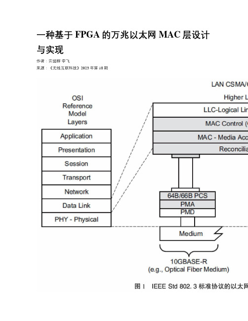
一种基于FPGA的万兆以太网MAC层设计与实现作者:安超群李飞来源:《无线互联科技》2023年第18期作者简介:安超群(1986—),女,湖北襄阳人,工程师,硕士;研究方向:模拟电路设计,集成电路设计,数字信号处理,可靠性设计等。
摘要:针对基于软件设计的万兆以太网MAC层无法满足高速数据实时传输的发展要求,文章提出了一种基于FPGA硬件平台的万兆以太网MAC层协议的设计与实现方案。
该设计方案主要利用FPGA的并行处理能力,通过Verilog硬件描述语言完成万兆以太网MAC层数据实时处理的硬件设计,实现大带宽、低延时和高可靠性的万兆以太网MAC层的数据收发功能。
试验验证表明:该设计方案实现了万兆以太网高速率的数据传输,具有低延时、高性能、高可靠性与简易性等优点。
关键词:万兆以太网;MAC控制器;并行CRC校验;并行数据处理中图分类号:TP311 文献标志码:A0 引言以太网(Ethernet)是一种计算机局域网技术。
IEEE制定的IEEE Std 802.3协议,规定了包括MAC层的协议内容、电信号以及物理层的连线。
从1983年第一次发布IEEE Std 802.3协议至今,以太网经过了40年的发展,传输速率从10 Mbps、100Mbps提升到1 000Mbps,目前已经达到了10 Gbps[1]。
万兆以太网是也称10 G以太网(10 Gigabit Ethernet),是在IEEE802.3ae协议中提出的以太网标准,该标准规范中规定使用光纤传输、传输带宽高达10 Gbps、传输距离最远能达到40km [2],经过不断的升级与扩充,万兆以太网以其速率高、兼容性好、稳定性强的优点逐渐成为以太网的核心设备[3],服务于工业自动化、5G网络传输和智慧城市建设等行业。
大多数系统设计中,10Mbps、100Mbps和1 000Mbps以太网协议除了物理层以外的协議层均以软件的方式实现,甚至10 Gbps以太网协议使用高性能CUP或服务器实现。

• 174•基于FPGA+CPU的信号处理系统的设计与实现上海广电通信技术有限公司 李红霞【摘要】文章简要介绍了雷达信号处理的发展现状,为了解决现有的雷达信号处理系统信号处理能力弱、数据传输速率低的问题,设计开发了基于FPGA+CPU 的船用导航雷达信号处理系统。
该系统充分利用FPGA 的流水性能以及通用 CPU 的并行处理能力,将算法合理分配至不同的处理器中,实现大数据量的实时传输和高性能的实时信号处理。
文章从系统设计入手介绍了船用导航雷达信号处理系统的工作原理,简要介绍了船用导航雷达信号处理系统的硬件设计,并从信号预处理、信号处理、目标跟踪三个方面阐述了船用导航雷达信号处理系统的信号处理流程和算法设计。
【关键词】雷达信号处理系统;信号预处理;信号处理;目标跟踪0 引言船舶驾驶员在驾驶船舶过程中,需要做到瞭望、定位、导航和避碰,这就要通过船用导航雷达来保证。
船用导航雷达是船舶正常航行所必备的电子设备之一,在过弯道、船舶靠港和离开以及海上作业等方面起到了重要的作用[1]。
雷达系统的不断升级相应的要求大幅提升信号处理系统的计算速度、数据带宽和传输速率[2]。
而现有的雷达信号处理系统的运算能力较低,传送数据的速率不高,无法满足现代信号处理的需求。
因此增强雷达系统的运算能力,提高传送数据的速度是如今雷达信号处理亟待解决的问题。
本文所采用的方案,可以很好地完成实时、可靠的雷达信号处理。
本文中的信号处理系统采用ADC+FPGA+CPU 的系统架构,集高密度计算与高速数据传输于一体,实现强大的信号处理及数据交换能力[1],同时提高了系统的集成度。
1 系统设计船用导航雷达信号处理的数据量大,对实时性和数据传输速率都要求较高,本文中针对以上特点,并结合 FPGA 的流水性能以及通用 CPU 的并行处理能力,将算法合理分配至不同的处理器中,提升了信号处理能力和数据传输能力,降低成本的同时提高了系统的集成度。
船用导航雷达信号处理系统通过ADC 对视频信号进行采样,将模拟视频信号转换为数字化的视频数据。


计算机工程与设计COMPUTER ENGINEERING AND DESIGNApr.2021Vol.42 No.42021年4月第42卷第4期基于RISC-V 的计算机系统综合实验设计孙卫真1!刘雪松朱威浦2 !向 勇3 +(1首都师范大学 信息工程学院,北京100048; 2.中国科学院计算技术研究所,北京101407;3.清华大学 计算机科学与技术系,北京100084)摘要:针对目前高校计算机系统各课程实验衔接不紧密、实验成本较高的问题!提出设计基于小型FPGA 开发板、以 RISC-V CPU 和Rut 操作系统内核为核心的计算机系统综合实验平台。
硬件实验以在低成本FPGA 芯片上搭建picorv32 RISC-V CPU 为核心!软件实验以在硬件实验基础上移植Rut 编写的rCore 教学操作系统为核心。
以较低成本在同一平台 完成计算机组成原理与操作系统实验设计!使其形成一个有机的整体,在资源与成本有限的情况下构建一个较为完整的实验体系。
实例结果表明!实验平台以软硬件协作的方式,适应技术的发展!及时更新实验内容!可满足高校计算机系统教学综合实验的基本要求。
关键词:RISC-V &系统编程语言;组成原理实验&操作系统实验&软硬件协作中图法分类号:TP301 文献标识号:A 文章编号:1000-7024 (2021 041159-07doi : 10. 16208/j. issnl 000-7024. 2021. 04. 037De?ign for comprehen?ive laboratory of computer?y?tem ba?ed onRISC-VSUN Wei-zhen 1, LIU Xue-song 1, ZHU Wei-pu 2, XIANG Yong 3+(1. I n f o r m a t i o n E n g i n e r i n g C o l e g e , C a p i t a l N o r m a l U n i v e r s i t y # B e i j n g 10048, C h i n a ;2. I n s t i u t e o f C o m p u t i n g T e c h n o l o g y , C h i n e s e A c a d e m y o f S c i e n c e s , B e i j n g 101407 , C h i n a ;3. Department of Computer Science and Technology , Tsinghua University , Beijing 100084 , China)Abstract: A i m i n g a t r y i n g t o i m p r o v e t h e e x p e r i m e n t a l c o n e c t i o n a m o n g t h e c o m p u t e r s y s t e m c o u r s e s i n t h e u n i v e r s i t e s a n d r e - d u c e t h e x p e r i m e n t c o s t #a c o m p r e h e n s i v e c o m p u t e r s y s t e m e x p e r i m e n t a l p l a t f o r m b a s e d o n a s m a lF PG Ab o a r d a n d a t e a c h i n g o p e r a t i o n s y s t e m w a s p r o p o s e d . T h e h a r d w a r e e x p e r i m e n t w a s b u i l d i n g a s y s t e m o n c h i p (S o C ) w i t h p i c o r v 32 R I S C -V C P U o n a l o w -c o s t F P G A c h i p . T h e s o f t w a r e e x p e r i m e n t w a s t r a n s p l a n t i n g t h e r C o r e t e a c h i n g o p e r a t i o n s y s t e m w r i t e n b y R u s t o n t h e i r o w n S o C . T h e c o m p u t e r c o m p o s i t o n p r i n c i p l e a n d o p e r a t i o n s y s t e m e x p e r i m e n t a l d e s i g n o n t h e s a m e p l a t f o r m a t a l o w e r c o s t wa s F o m p l e t e d #a n d a n o r g a n i F w h o l e w a s f o r m e d . T h e e x p e r i m e n t a l s y s t e m w a s a r e l a t i v e F o m p l e t e p l a t f o r m w i t h l i m i t e d F o s t s . E x a m p l e s h o w t h a t #t h e x p e r i m e n t a l F o n t e n t s a r e t i m e l y u p d a t e d f o r t r a F i n g F o m p u t e r t e F h n o l o g y t r e n d s i n a s o f t w a r e -h a r d - w a r e c o p e r a t i v e m a n e r t o m e t h e b a s i c r e q u i r e m e n t s o f c o m p u t e r s y s t e m t e a c h i n g e x p e r i m e n t s i n u n i v e r s i t e s .Keywords :RI S C -V ; s y s t e m p r o g r a m mi n g l a n g u a g e ; c o m p o s i t o n p r i n c i p l e e x p e r i m e n t ; o p e r a t i n g s y s t e m e x p e r i m e n t ; s o f t w a r e h a r d w a r e c o p e r a t i v e4引言目前,高校进行计算机系统教学实验主要有以下几种教学方式:其一是使用纯硬件搭建实验平台,虽该方式可深入接触计算机硬件模块,但实验操作机械死板、硬件平台开发成本较高;其二是采用软件系统仿真的方式,该方法成本较低、易于上手,但受教育者不能在实验过程中较好体会到计算机与硬件的紧密结合!为了优化上述问题,实现设计目标,本文从硬件支持、 处理器构建、系统编程语言选择三方面考虑,构建计算机 系统实验平台。
Verilog的135个经典设计实例王金明:《Verilog HDL程序设计教程》【例3.1】4位全加器module adder4(cout,sum,ina,inb,cin);output[3:0] sum;output cout;input[3:0] ina,inb;input cin;assign {cout,sum}=ina+inb+cin;endmodule【例3.2】4位计数器module count4(out,reset,clk);output[3:0] out;input reset,clk;reg[3:0] out;always @(posedge clk)beginif (reset) out<=0; //同步复位else out<=out+1; //计数endendmodule【例3.3】4位全加器的仿真程序`timescale 1ns/1ns`include "adder4.v"module adder_tp; //测试模块的名字reg[3:0] a,b; //测试输入信号定义为reg型reg cin;wire[3:0] sum; //测试输出信号定义为wire型wire cout;integer i,j;adder4 adder(sum,cout,a,b,cin); //调用测试对象always #5 cin=~cin; //设定cin的取值initialbegina=0;b=0;cin=0;for(i=1;i<16;i=i+1)#10 a=i; //设定a的取值end- 1 - 程序文本initialbeginfor(j=1;j<16;j=j+1)#10 b=j; //设定b的取值endinitial //定义结果显示格式begin$monitor($time,,,"%d + %d + %b={%b,%d}",a,b,cin,cout,sum);#160 $finish;endendmodule【例3.4】4位计数器的仿真程序`timescale 1ns/1ns`include "count4.v"module coun4_tp;reg clk,reset; //测试输入信号定义为reg型wire[3:0] out; //测试输出信号定义为wire型parameter DELY=100;count4 mycount(out,reset,clk); //调用测试对象always #(DELY/2) clk = ~clk; //产生时钟波形initialbegin //激励信号定义clk =0; reset=0;#DELY reset=1;#DELY reset=0;#(DELY*20) $finish;end//定义结果显示格式initial $monitor($time,,,"clk=%d reset=%d out=%d", clk, reset,out);endmodule【例3.5】“与-或-非”门电路module AOI(A,B,C,D,F); //模块名为AOI(端口列表A,B,C,D,F)input A,B,C,D; //模块的输入端口为A,B,C,Doutput F; //模块的输出端口为F- 2 -王金明:《Verilog HDL程序设计教程》wire A,B,C,D,F; //定义信号的数据类型assign F= ~((A&B)|(C&D)); //逻辑功能描述endmodule【例5.1】用case语句描述的4选1数据选择器module mux4_1(out,in0,in1,in2,in3,sel);output out;input in0,in1,in2,in3;input[1:0] sel;reg out;always @(in0 or in1 or in2 or in3 or sel) //敏感信号列表case(sel)2'b00: out=in0;2'b01: out=in1;2'b10: out=in2;2'b11: out=in3;default: out=2'bx;endcaseendmodule【例5.2】同步置数、同步清零的计数器module count(out,data,load,reset,clk);output[7:0] out;input[7:0] data;input load,clk,reset;reg[7:0] out;always @(posedge clk) //clk上升沿触发beginif (!reset) out = 8'h00; //同步清0,低电平有效else if (load) out = data; //同步预置else out = out + 1; //计数endendmodule【例5.3】用always过程语句描述的简单算术逻辑单元`define add 3'd0`define minus 3'd1`define band 3'd2`define bor 3'd3`define bnot 3'd4- 3 - 程序文本module alu(out,opcode,a,b);output[7:0] out;reg[7:0] out;input[2:0] opcode; //操作码input[7:0] a,b; //操作数always@(opcode or a or b) //电平敏感的always块begincase(opcode)`add: out = a+b; //加操作`minus: out = a-b; //减操作`band: out = a&b; //求与`bor: out = a|b; //求或`bnot: out=~a; //求反default: out=8'hx; //未收到指令时,输出任意态endcaseendendmodule【例5.4】用initial过程语句对测试变量A、B、C赋值`timescale 1ns/1nsmodule test;reg A,B,C;initialbeginA = 0;B = 1;C = 0;#50 A = 1; B = 0;#50 A = 0; C = 1;#50 B = 1;#50 B = 0; C = 0;#50 $finish ;endendmodule【例5.5】用begin-end串行块产生信号波形`timescale 10ns/1nsmodule wave1;reg wave;parameter cycle=10;initialbegin- 4 -王金明:《Verilog HDL程序设计教程》wave=0;#(cycle/2) wave=1;#(cycle/2) wave=0;#(cycle/2) wave=1;#(cycle/2) wave=0;#(cycle/2) wave=1;#(cycle/2) $finish ;endinitial $monitor($time,,,"wave=%b",wave); endmodule【例5.6】用fork-join并行块产生信号波形`timescale 10ns/1nsmodule wave2;reg wave;parameter cycle=5;initialforkwave=0;#(cycle) wave=1;#(2*cycle) wave=0;#(3*cycle) wave=1;#(4*cycle) wave=0;#(5*cycle) wave=1;#(6*cycle) $finish;initial $monitor($time,,,"wave=%b",wave); endmodule【例5.7】持续赋值方式定义的2选1多路选择器module MUX21_1(out,a,b,sel);input a,b,sel;output out;assign out=(sel==0)?a:b;//持续赋值,如果sel为0,则out=a ;否则out=b endmodule【例5.8】阻塞赋值方式定义的2选1多路选择器module MUX21_2(out,a,b,sel);input a,b,sel;- 5 - 程序文本output out;reg out;always@(a or b or sel)beginif(sel==0) out=a; //阻塞赋值else out=b;endendmodule【例5.9】非阻塞赋值module non_block(c,b,a,clk);output c,b;input clk,a;reg c,b;always @(posedge clk)beginb<=a;endendmodule【例5.10】阻塞赋值module block(c,b,a,clk);output c,b;input clk,a;reg c,b;always @(posedge clk)beginb=a;c=b;endendmodule【例5.11】模为60的BCD码加法计数器module count60(qout,cout,data,load,cin,reset,clk); output[7:0] qout;output cout;input[7:0] data;input load,cin,clk,reset;reg[7:0] qout;always @(posedge clk) //clk上升沿时刻计数- 6 - 王金明:《Verilog HDL程序设计教程》beginif (reset) qout<=0; //同步复位else if(load) qout<=data; //同步置数else if(cin)beginif(qout[3:0]==9) //低位是否为9,是则beginqout[3:0]<=0; //回0,并判断高位是否为5if (qout[7:4]==5) qout[7:4]<=0;elseqout[7:4]<=qout[7:4]+1; //高位不为5,则加1endelse //低位不为9,则加1qout[3:0]<=qout[3:0]+1;endendassign cout=((qout==8'h59)&cin)?1:0; //产生进位输出信号endmodule【例5.12】BCD码—七段数码管显示译码器module decode4_7(decodeout,indec);output[6:0] decodeout;input[3:0] indec;reg[6:0] decodeout;always @(indec)begincase(indec) //用case语句进行译码4'd0:decodeout=7'b1111110;4'd1:decodeout=7'b0110000;4'd2:decodeout=7'b1101101;4'd3:decodeout=7'b1111001;4'd4:decodeout=7'b0110011;4'd5:decodeout=7'b1011011;4'd6:decodeout=7'b1011111;4'd7:decodeout=7'b1110000;4'd8:decodeout=7'b1111111;4'd9:decodeout=7'b1111011;default: decodeout=7'bx;endcaseend- 7 - 程序文本endmodule【例5.13】用casez描述的数据选择器module mux_casez(out,a,b,c,d,select); output out;input a,b,c,d;input[3:0] select;reg out;always @(select or a or b or c or d) begincasez(select)4'b1: out = a;4'b??1?: out = b;4'b?1??: out = c;4'b1: out = d;endcaseendendmodule【例5.14】隐含锁存器举例module buried_ff(c,b,a);output c;input b,a;reg c;always @(a or b)beginif((b==1)&&(a==1)) c=a&b;endendmodule【例5.15】用for语句描述的七人投票表决器module voter7(pass,vote);output pass;input[6:0] vote;reg[2:0] sum;integer i;reg pass;always @(vote)beginsum=0;- 8 -王金明:《Verilog HDL程序设计教程》for(i=0;i<=6;i=i+1) //for语句if(vote[i]) sum=sum+1;if(sum[2]) pass=1; //若超过4人赞成,则pass=1 else pass=0;endendmodule【例5.16】用for语句实现2个8位数相乘module mult_for(outcome,a,b);parameter size=8;input[size:1] a,b; //两个操作数output[2*size:1] outcome; //结果reg[2*size:1] outcome;integer i;always @(a or b)beginoutcome=0;for(i=1; i<=size; i=i+1) //for语句if(b[i]) outcome=outcome +(a << (i-1));endendmodule【例5.17】用repeat实现8位二进制数的乘法module mult_repeat(outcome,a,b);parameter size=8;input[size:1] a,b;output[2*size:1] outcome;reg[2*size:1] temp_a,outcome;reg[size:1] temp_b;always @(a or b)beginoutcome=0;temp_a=a;temp_b=b;repeat(size) //repeat语句,size为循环次数beginif(temp_b[1]) //如果temp_b的最低位为1,就执行下面的加法outcome=outcome+temp_a;temp_a=temp_a<<1; //操作数a左移一位- 9 - 程序文本temp_b=temp_b>>1; //操作数b右移一位endendendmodule【例5.18】同一循环的不同实现方式module loop1; //方式1integer i;initialfor(i=0;i<4;i=i+1) //for语句begin$display(“i=%h”,i);endendmodulemodule loop2; //方式2integer i;initial begini=0;while(i<4) //while语句begin$display ("i=%h",i);i=i+1;endendendmodulemodule loop3; //方式3integer i;initial begini=0;repeat(4) //repeat语句begin$display ("i=%h",i);i=i+1;endendendmodule【例5.19】使用了`include语句的16位加法器- 10 -王金明:《Verilog HDL程序设计教程》`include "adder.v" module adder16(cout,sum,a,b,cin);output cout;parameter my_size=16;output[my_size-1:0] sum;input[my_size-1:0] a,b;input cin;adder my_adder(cout,sum,a,b,cin); //调用adder模块endmodule//下面是adder模块代码module adder(cout,sum,a,b,cin);parameter size=16;output cout;output[size-1:0] sum;input cin;input[size-1:0] a,b;assign {cout,sum}=a+b+cin;endmodule【例5.20】条件编译举例module compile(out,A,B);output out;input A,B;`ifdef add //宏名为addassign out=A+B;`elseassign out=A-B;`endifendmodule【例6.1】加法计数器中的进程module count(data,clk,reset,load,cout,qout);output cout;output[3:0] qout;reg[3:0] qout;input[3:0] data;input clk,reset,load;- 11 - 程序文本always @(posedge clk) //进程1,always过程块beginif (!reset) qout= 4'h00; //同步清0,低电平有效else if (load) qout= data; //同步预置else qout=qout + 1; //加法计数endassign cout=(qout==4'hf)?1:0; //进程2,用持续赋值产生进位信号endmodule【例6.2】任务举例module alutask(code,a,b,c);input[1:0] code;input[3:0] a,b;output[4:0] c;reg[4:0] c;task my_and; //任务定义,注意无端口列表input[3:0] a,b; //a,b,out名称的作用域范围为task任务内部output[4:0] out;integer i;beginfor(i=3;i>=0;i=i-1)out[i]=a[i]&b[i]; //按位与endendtaskalways@(code or a or b)begincase(code)2'b00: my_and(a,b,c);/* 用任务my_and,需注意端口列表的顺序应与任务定义中的一致,这里的a,b,c分别对应任务定义中的a,b,out */2'b01: c=a|b; //或2'b10: c=a-b; //相减2'b11: c=a+b; //相加endcaseendendmodule- 12 -王金明:《Verilog HDL程序设计教程》【例6.3】测试程序`include "alutask.v"module alu_tp;reg[3:0] a,b;reg[1:0] code;wire[4:0] c;parameter DELY = 100;alutask ADD(code,a,b,c); //调用被测试模块initial begincode=4'd0; a= 4'b0000; b= 4'b1111;#DELY code=4'd0; a= 4'b0111; b= 4'b1101;#DELY code=4'd1; a= 4'b0001; b= 4'b0011;#DELY code=4'd2; a= 4'b1001; b= 4'b0011;#DELY code=4'd3; a= 4'b0011; b= 4'b0001;#DELY code=4'd3; a= 4'b0111; b= 4'b1001;#DELY $finish;endinitial $monitor($time,,,"code=%b a=%b b=%b c=%b", code,a,b,c);endmodule【例6.4】函数function[7:0] get0;input[7:0] x;reg[7:0] count;integer i;begincount=0;for (i=0;i<=7;i=i+1)if (x[i]=1'b0) count=count+1;get0=count;endendfunction【例6.5】用函数和case语句描述的编码器(不含优先顺序)module code_83(din,dout);input[7:0] din;output[2:0] dout;- 13 - 程序文本function[2:0] code; //函数定义input[7:0] din; //函数只有输入,输出为函数名本身casex (din)8'b1xxx_xxxx : code = 3'h7;8'b01xx_xxxx : code = 3'h6;8'b001x_xxxx : code = 3'h5;8'b0001_xxxx : code = 3'h4;8'b0000_1xxx : code = 3'h3;8'b0000_01xx : code = 3'h2;8'b0000_001x : code = 3'h1;8'b0000_000x : code = 3'h0;default: code = 3'hx;endcaseendfunctionassign dout = code(din) ; //函数调用endmodule【例6.6】阶乘运算函数module funct(clk,n,result,reset);output[31:0] result;input[3:0] n;input reset,clk;reg[31:0] result;always @(posedge clk) //在clk的上升沿时执行运算beginif(!reset) result<=0; //复位else beginresult <= 2 * factorial(n); //调用factorial函数endendfunction[31:0] factorial; //阶乘运算函数定义(注意无端口列表)input[3:0] opa; //函数只能定义输入端,输出端口为函数名本身reg[3:0] i;beginfactorial = opa ? 1 : 0;for(i= 2; i <= opa; i = i+1) //该句若要综合通过,opa应赋具体的数值factorial = i* factorial; //阶乘运算end- 14 -王金明:《Verilog HDL程序设计教程》endfunction【例6.7】测试程序`define clk_cycle 50`include "funct.v"module funct_tp;reg[3:0] n;reg reset,clk;wire[31:0] result;initial //定义激励向量beginn=0; reset=1; clk=0;for(n=0;n<=15;n=n+1)#100 n=n;endinitial $monitor($time,,,"n=%d result=%d",n,result);//定义输出显示格式always # `clk_cycle clk=~clk; //产生时钟信号funct funct_try(.clk(clk),.n(n),.result(result),.reset(reset)); //调用被测试模块endmodule【例6.8】顺序执行模块1module serial1(q,a,clk);output q,a;input clk;reg q,a;always @(posedge clk)beginq=~q;a=~q;end【例6.9】顺序执行模块2 module serial2(q,a,clk); output q,a;- 15 - 程序文本input clk;reg q,a;always @(posedge clk) begina=~q;q=~q;endendmodule【例6.10】并行执行模块1 module paral1(q,a,clk); output q,a;input clk;reg q,a;always @(posedge clk) beginq=~q;endalways @(posedge clk) begina=~q;endendmodule【例6.11】并行执行模块2 module paral2(q,a,clk); output q,a;input clk;reg q,a;always @(posedge clk)begina=~q;endalways @(posedge clk)beginq=~q;endendmodule【例7.1】调用门元件实现的4选1 MUX- 16 -王金明:《Verilog HDL程序设计教程》module mux4_1a(out,in1,in2,in3,in4,cntrl1,cntrl2);output out;input in1,in2,in3,in4,cntrl1,cntrl2;wire notcntrl1,notcntrl2,w,x,y,z;not notcntrl1,cntrl2),(notcntrl2,cntrl2);and (w,in1,notcntrl1,notcntrl2),(x,in2,notcntrl1,cntrl2),(y,in3,cntrl1,notcntrl2),(z,in4,cntrl1,cntrl2);or (out,w,x,y,z);endmodule【例7.2】用case语句描述的4选1 MUXmodule mux4_1b(out,in1,in2,in3,in4,cntrl1,cntrl2);output out;input in1,in2,in3,in4,cntrl1,cntrl2;reg out;always@(in1 or in2 or in3 or in4 or cntrl1 or cntrl2)case({cntrl1,cntrl2})2'b00:out=in1;2'b01:out=in2;2'b10:out=in3;2'b11:out=in4;default:out=2'bx;endcaseendmodule【例7.3】行为描述方式实现的4位计数器module count4(clk,clr,out);input clk,clr;output[3:0] out;reg[3:0] out;always @(posedge clk or posedge clr)beginif (clr) out<=0;else out<=out+1;endendmodule- 17 - 程序文本【例7.4】数据流方式描述的4选1 MUXmodule mux4_1c(out,in1,in2,in3,in4,cntrl1,cntrl2);output out;input in1,in2,in3,in4,cntrl1,cntrl2;assign out=(in1 & ~cntrl1 & ~cntrl2)|(in2 & ~cntrl1 & cntrl2)|(in3 & cntrl1 & ~cntrl2)|(in4 & cntrl1 & cntrl2);endmodule【例7.5】用条件运算符描述的4选1 MUXmodule mux4_1d(out,in1,in2,in3,in4,cntrl1,cntrl2); output out;input in1,in2,in3,in4,cntrl1,cntrl2;assign out=cntrl1 ? (cntrl2 ? in4:in3):(cntrl2 ? in2:in1); endmodule【例7.6】门级结构描述的2选1MUXmodule mux2_1a(out,a,b,sel);output out;input a,b,sel;not (sel_,sel);and a1,a,sel_),(a2,b,sel);or (out,a1,a2);endmodule【例7.7】行为描述的2选1MUXmodule mux2_1b(out,a,b,sel);output out;input a,b,sel;reg out;always @(a or b or sel)beginif(sel) out = b;else out = a;endendmodule【例7.8】数据流描述的2选1MUXmodule MUX2_1c(out,a,b,sel);output out;- 18 -王金明:《Verilog HDL程序设计教程》input a,b,sel;assign out = sel ? b : a; endmodule【例7.9】调用门元件实现的1位半加器module half_add1(a,b,sum,cout); input a,b;output sum,cout;and cout,a,b);xor sum,a,b);endmodule【例7.10】数据流方式描述的1位半加器module half_add2(a,b,sum,cout); input a,b;output sum,cout;assign sum=a^b;assign cout=a&b;endmodule【例7.11】采用行为描述的1位半加器module half_add3(a,b,sum,cout); input a,b;output sum,cout;reg sum,cout;always @(a or b)begincase ({a,b}) //真值表描述2'b00: begin sum=0; cout=0; end2'b01: begin sum=1; cout=0; end2'b10: begin sum=1; cout=0; end2'b11: begin sum=0; cout=1; end endcaseendendmodule【例7.12】采用行为描述的1位半加器module half_add4(a,b,sum,cout); input a,b;output sum,cout;- 19 - 程序文本reg sum,cout;always @(a or b)beginsum= a^b;cout=a&b;endendmodule【例7.13】调用门元件实现的1位全加器module full_add1(a,b,cin,sum,cout); input a,b,cin;output sum,cout;wire s1,m1,m2,m3;and m1,a,b),(m2,b,cin),(m3,a,cin);xor s1,a,b),(sum,s1,cin);or (cout,m1,m2,m3);endmodule【例7.14】数据流描述的1位全加器module full_add2(a,b,cin,sum,cout); input a,b,cin;output sum,cout;assign sum = a ^ b ^ cin;assign cout = (a & b)|(b & cin)|(cin & a);endmodule【例7.15】1位全加器module full_add3(a,b,cin,sum,cout);input a,b,cin;output sum,cout;assign {cout,sum}=a+b+cin;endmodule【例7.16】行为描述的1位全加器module full_add4(a,b,cin,sum,cout);input a,b,cin;output sum,cout;- 20 -王金明:《Verilog HDL程序设计教程》reg sum,cout; //在always块中被赋值的变量应定义为reg型reg m1,m2,m3;always @(a or b or cin)beginsum = (a ^ b) ^ cin;m1 = a & b;m2 = b & cin;m3 = a & cin;cout = (m1|m2)|m3;endendmodule【例7.17】混合描述的1位全加器module full_add5(a,b,cin,sum,cout);input a,b,cin;output sum,cout;reg cout,m1,m2,m3; //在always块中被赋值的变量应定义为reg型wire s1;xor x1(s1,a,b); //调用门元件always @(a or b or cin) //always块语句beginm1 = a & b;m2 = b & cin;m3 = a & cin;cout = (m1| m2) | m3;endassign sum = s1 ^ cin; //assign持续赋值语句endmodule【例7.18】结构描述的4位级连全加器`include "full_add1.v"module add4_1(sum,cout,a,b,cin);output[3:0] sum;output cout;input[3:0] a,b;input cin;full_add1 f0(a[0],b[0],cin,sum[0],cin1); //级连描述full_add1 f1(a[1],b[1],cin1,sum[1],cin2);full_add1 f2(a[2],b[2],cin2,sum[2],cin3);- 21 - 程序文本full_add1 f3(a[3],b[3],cin3,sum[3],cout); endmodule【例7.19】数据流描述的4位全加器module add4_2(cout,sum,a,b,cin);output[3:0] sum;output cout;input[3:0] a,b;input cin;assign {cout,sum}=a+b+cin;endmodule【例7.20】行为描述的4位全加器module add4_3(cout,sum,a,b,cin);output[3:0] sum;output cout;input[3:0] a,b;input cin;reg[3:0] sum;reg cout;always @(a or b or cin)begin{cout,sum}=a+b+cin;endendmodule【例8.1】$time与$realtime的区别`timescale 10ns/1nsmodule time_dif;reg ts;parameter delay=2.6;initialbegin#delay ts=1;#delay ts=0;#delay ts=1;#delay ts=0;endinitial $monitor($time,,,"ts=%b",ts); //使用函数$time- 22 - 王金明:《Verilog HDL程序设计教程》endmodule【例8.2】$random函数的使用`timescale 10ns/1nsmodule random_tp;integer data;integer i;parameter delay=10;initial $monitor($time,,,"data=%b",data);initial beginfor(i=0; i<=100; i=i+1)#delay data=$random; //每次产生一个随机数endendmodule【例8.3】1位全加器进位输出UDP元件primitive carry_udp(cout,cin,a,b);input cin,a,b;output cout;table//cin a b : cout //真值表0 0 0 : 0;0 1 0 : 0;0 0 1 : 0;0 1 1 : 1;1 0 0 : 0;1 0 1 : 1;1 1 0 : 1;1 1 1 : 1;endtableendprimitive【例8.4】包含x态输入的1位全加器进位输出UDP元件primitive carry_udpx1(cout,cin,a,b);input cin,a,b;output cout;table// cin a b : cout //真值表0 0 0 : 0;- 23 - 程序文本0 1 0 : 0;0 0 1 : 0;0 1 1 : 1;1 0 0 : 0;1 0 1 : 1;1 1 0 : 1;1 1 1 : 1;0 0 x : 0; //只要有两个输入为0,则进位输出肯定为0 0 x 0 : 0;x 0 0 : 0;1 1 x : 1; //只要有两个输入为1,则进位输出肯定为1 1 x 1 : 1;x 1 1 : 1;endtableendprimitive【例8.5】用简缩符“?”表述的1位全加器进位输出UDP元件primitive carry_udpx2(cout,cin,a,b);input cin,a,b;output cout;table// cin a b : cout //真值表0 0 : 0; //只要有两个输入为0,则进位输出肯定为00 ? 0 : 0;0 0 ? : 0;1 1 : 1; //只要有两个输入为1,则进位输出肯定为11 ? 1 : 1;1 1 ? : 1;endtableendprimitive【例8.6】3选1多路选择器UDP元件primitive mux31(Y,in0,in1,in2,s2,s1);input in0,in1,in2,s2,s1;output Y;table//in0 in1 in2 s2 s1 : Y0 ? ? 0 0 : 0; //当s2s1=00时,Y=in01 ? ? 0 0 : 1;0 ? 0 1 : 0; //当s2s1=01时,Y=in1 - 24 -王金明:《Verilog HDL程序设计教程》1 ? 0 1 : 1;0 1 ? : 0; //当s2s1=1?时,Y=in21 1 ? : 1;0 0 ? 0 ? : 0;1 1 ? 0 ? : 1;0 ? 0 ? 0 : 0;1 ? 1 ? 0 : 1;0 0 ? 1 : 0;1 1 ? 1 : 1;endtableendprimitive【例8.7】电平敏感的1位数据锁存器UDP元件primitive latch(Q,clk,reset,D);input clk,reset,D;output Q;reg Q;initial Q = 1'b1; //初始化table// clk reset D : state : Q1 ? : ? : 0 ; //reset=1,则不管其他端口为什么值,输出都为00 0 0 : ? : 0 ; //clk=0,锁存器把D端的输入值输出0 0 1 : ? : 1 ;1 0 ? : ? : - ; //clk=1,锁存器的输出保持原值,用符号“-”表示endtableendprimitive【例8.8】上升沿触发的D触发器UDP元件primitive DFF(Q,D,clk);output Q;input D,clk;reg Q;table//clk D : state : Q(01) 0 : ? : 0; //上升沿到来,输出Q=D(01) 1 : ? : 1;(0x) 1 : 1 : 1;(0x) 0 : 0 : 0;(?0) ? : ? : -; //没有上升沿到来,输出Q保持原值(??) : ? : - ; //时钟不变,输出也不变- 25 - 程序文本endtableendprimitive【例8.9】带异步置1和异步清零的上升沿触发的D触发器UDP 元件primitive DFF_UDP(Q,D,clk,clr,set);output Q;input D,clk,clr,set;reg Q;table// clk D clr et state : Q (01) 1 0 0 : ? : 0; (01) 1 0 x : ? : 0;0 x : 0 : 0;(01) 0 0 0 : ? : 1; (01) 0 x 0 : ? : 1;x 0 : 1 : 1;(x1) 1 0 0 : 0 : 0;(x1) 0 0 0 : 1 : 1;(0x) 1 0 0 : 0 : 0;(0x) 0 0 0 : 1 : 1;1 ? : ? : 1; //异步复位0 1 : ? : 0; //异步置1 n ? 0 0 : ? : -;* ? ? : ? : -;(?0) ? : ? : -;(?0): ? : -;: ? : x;endtableendprimitive【例8.12】延迟定义块举例module delay(out,a,b,c); output out;input a,b,c;and a1(n1,a,b);or o1(out,c,n1);specify(a=>out)=2;(b=>out)=3;(c=>out)=1;- 26 -王金明:《Verilog HDL程序设计教程》endspecifyendmodule【例8.13】激励波形的描述'timescale 1ns/1nsmodule test1;reg A,B,C;initialbegin //激励波形描述A = 0;B = 1;C = 0;#100 C = 1;#100 A = 1; B = 0;#100 A = 0;#100 C = 0;#100 $finish;endinitial $monitor($time,,,"A=%d B=%d C=%d",A,B,C); //显示endmodule【例8.15】用always过程块产生两个时钟信号module test2;reg clk1,clk2;parameter CYCLE = 100;alwaysbegin{clk1,clk2} = 2'b10;#(CYCLE/4) {clk1,clk2} = 2'b01;#(CYCLE/4) {clk1,clk2} = 2'b11;#(CYCLE/4) {clk1,clk2} = 2'b00;#(CYCLE/4) {clk1,clk2} = 2'b10;endinitial $monitor($time,,,"clk1=%b clk2=%b",clk1,clk2); endmodule【例8.17】存储器在仿真程序中的应用module ROM(addr,data,oe);output[7:0] data; //数据信号input[14:0] addr; //地址信号input oe; //读使能信号,低电平有效- 27 - 程序文本reg[7:0] mem[0:255]; //存储器定义parameter DELAY = 100;assign #DELAY data=(oe==0) ? mem[addr] : 8'hzz; initial $readmemh("rom.hex",mem); //从文件中读入数据endmodule【例8.18】8位乘法器的仿真程序`timescale 10ns/1nsmodule mult_tp; //测试模块的名字reg[7:0] a,b; //测试输入信号定义为reg型wire [15:0] out; //测试输出信号定义为wire型integer i,j;mult8 m1(out,a,b); //调用测试对象//激励波形设定initialbegina=0;b=0;for(i=1;i<255;i=i+1)#10 a=i;endinitialbeginfor(j=1;j<255;j=j+1)#10 b=j;endinitial //定义结果显示格式begin$monitor($time,,,"%d * %d= %d",a,b,out);#2560 $finish;endendmodulemodule mult8(out, a, b); //8位乘法器源代码parameter size=8;input[size:1] a,b; //两个操作数output[2*size:1] out; //结果assign out=a*b; //乘法运算符- 28 -王金明:《Verilog HDL程序设计教程》endmodule 【例8.19】8位加法器的仿真程序`timescale 1ns/1nsmodule add8_tp; //仿真模块无端口列表reg[7:0] A,B; //输入激励信号定义为reg型reg cin;wire[7:0] SUM; //输出信号定义为wire型wire cout;parameter DELY = 100;add8 AD1(SUM,cout,A,B,cin); //调用测试对象initial begin //激励波形设定A= 8'd0; B= 8'd0; cin=1'b0;#DELY A= 8'd100; B= 8'd200; cin=1'b1;#DELY A= 8'd200; B= 8'd88;#DELY A= 8'd210; B= 8'd18; cin=1'b0;#DELY A= 8'd12; B= 8'd12;#DELY A= 8'd100; B= 8'd154;#DELY A= 8'd255; B= 8'd255; cin=1'b1;#DELY $finish;end//输出格式定义initial $monitor($time,,,"%d + %d + %b = {%b, %d}",A,B,cin,cout,SUM);endmodulemodule add8(SUM,cout,A,B,cin); //待测试的8位加法器模块output[7:0] SUM;output cout;input[7:0] A,B;input cin;assign {cout,SUM}=A+B+cin;endmodule【例8.20】2选1多路选择器的仿真`timescale 1ns/1nsmodule mux_tp;reg a,b,sel;wire out;- 29 - 程序文本MUX2_1 m1(out,a,b,sel); //调用待测试模块initialbegina=1'b0; b=1'b0; sel=1'b0;#5 sel=1'b1;#5 a=1'b1; el=1'b0;#5 sel=1'b1;#5 a=1'b0; b=1'b1; el=1'b0;#5 sel=1'b1;#5 a=1'b1; b=1'b1; sel=1'b0;#5 sel=1'b1;endinitial $monitor($time,,,"a=%b b=%b sel=%b out=%b",a,b,sel,out);endmodulemodule MUX2_1(out,a,b,sel); //待测试的2选1MUX模块input a,b,sel;output out;not #(0.4,0.3) (sel_,sel); //#(0.4,0.3)为门延时and #(0.7,0.6) (a1,a,sel_);and #(0.7,0.6) (a2,b,sel);or #(0.7,0.6) (out,a1,a2);endmodule【例8.21】8位计数器的仿真`timescale 10ns/1nsmodule count8_tp;reg clk,reset; //输入激励信号定义为reg型wire[7:0] qout; //输出信号定义为wire型parameter DELY=100;counter C1(qout,reset,clk); //调用测试对象always #(DELY/2) clk = ~clk; //产生时钟波形initialbegin //激励波形定义clk =0; reset=0;- 30 -王金明:《Verilog HDL程序设计教程》#DELY reset=1;#DELY reset=0;#(DELY*300) $finish;end//结果显示initial $monitor($time,,,"clk=%d reset=%d qout=%d",clk,reset,qout);endmodulemodule counter(qout,reset,clk); //待测试的8位计数器模块output[7:0] qout;input clk,reset;reg[7:0] qout;always @(posedge clk)begin if (reset) qout<=0;else qout<=qout+1;endendmodule【例9.1】基本门电路的几种描述方法(1)门级结构描述module gate1(F,A,B,C,D);input A,B,C,D;output F;nand(F1,A,B); //调用门元件and(F2,B,C,D);or(F,F1,F2);endmodule(2)数据流描述module gate2(F,A,B,C,D);input A,B,C,D;output F;assign F=(A&B)|(B&C&D); //assign持续赋值endmodule(3)行为描述module gate3(F,A,B,C,D);input A,B,C,D;output F;- 31 - 程序文本reg F;always @(A or B or C or D) //过程赋值beginF=(A&B)|(B&C&D);endendmodule【例9.2】用bufif1关键字描述的三态门module tri_1(in,en,out);input in,en;output out;tri out;bufif1 b1(out,in,en); //注意三态门端口的排列顺序endmodule【例9.3】用assign语句描述的三态门module tri_2(out,in,en);output out;input in,en;assign out = en ? in : 'bz;//若en=1,则out=in;若en=0,则out为高阻态endmodule【例9.4】三态双向驱动器module bidir(tri_inout,out,in,en,b);inout tri_inout;output out;input in,en,b;assign tri_inout = en ? in : 'bz;assign out = tri_inout ^ b; endmodule【例9.5】三态双向驱动器module bidir2(bidir,en,clk);inout[7:0] bidir;input en,clk;reg[7:0] temp;assign bidir= en ? temp : 8'bz; always @(posedge clk)begin- 32 -王金明:《Verilog HDL程序设计教程》if(en) temp=bidir;else temp=temp+1;endendmodule【例9.6】3-8译码器module decoder_38(out,in);output[7:0] out;input[2:0] in;reg[7:0] out;always @(in)begincase(in)3'd0: out=8'b11111110;3'd1: out=8'b11111101;3'd2: out=8'b11111011;3'd3: out=8'b11110111;3'd4: out=8'b11101111;3'd5: out=8'b11011111;3'd6: out=8'b10111111;3'd7: out=8'b01111111;endcaseendendmodule【例9.7】8-3优先编码器module encoder8_3(none_on,outcode,a,b,c,d,e,f,g,h); output none_on;output[2:0] outcode;input a,b,c,d,e,f,g,h;reg[3:0] outtemp;assign {none_on,outcode}=outtemp;always @(a or b or c or d or e or f or g or h)beginif(h) outtemp=4'b0111;else if(g) outtemp=4'b0110;else if(f) outtemp=4'b0101;else if(e) outtemp=4'b0100;else if(d) outtemp=4'b0011;else if(c) outtemp=4'b0010;- 33 - 程序文本else if(b) outtemp=4'b0001;else if(a) outtemp=4'b0000;else outtemp=4'b1000;endendmodule【例9.8】用函数定义的8-3优先编码器module code_83(din, dout);input[7:0] din;output[2:0] dout;function[2:0] code; //函数定义input[7:0] din; //函数只有输入端口,输出为函数名本身if (din[7]) code = 3'd7;else if (din[6]) code = 3'd6;else if (din[5]) code = 3'd5;else if (din[4]) code = 3'd4;else if (din[3]) code = 3'd3;else if (din[2]) code = 3'd2;else if (din[1]) code = 3'd1;else code = 3'd0;endfunctionassign dout = code(din); //函数调用endmodule【例9.9】七段数码管译码器module decode47(a,b,c,d,e,f,g,D3,D2,D1,D0);output a,b,c,d,e,f,g;input D3,D2,D1,D0; //输入的4位BCD码reg a,b,c,d,e,f,g;always @(D3 or D2 or D1 or D0)begincase({D3,D2,D1,D0}) //用case语句进行译码4'd0: {a,b,c,d,e,f,g}=7'b1111110;4'd1: {a,b,c,d,e,f,g}=7'b0110000;4'd2: {a,b,c,d,e,f,g}=7'b1101101;4'd3: {a,b,c,d,e,f,g}=7'b1111001;4'd4: {a,b,c,d,e,f,g}=7'b0110011;4'd5: {a,b,c,d,e,f,g}=7'b1011011;- 34 -王金明:《Verilog HDL程序设计教程》4'd6: {a,b,c,d,e,f,g}=7'b1011111;。
基于VerilogHDL的简单CPU设计摘要:本文实现了一个基于veriloghdl的简单cpu,系统由运算器、控制器、译码器、存储器、指令计数器五大模块构成。
在对各个模块时序仿真实验的基础上,系统整体功能测试成功。
系统具有良好的稳定性和灵活性,指令集易扩展。
关键词:veriloghdl;cpu;时序仿真中图分类号:tp3341 引言veriloghdl【1】是一种硬件描述语言(hdl:hardwarediscriptionlanguage),是一种以文本形式来描述数字系统硬件的结构和行为的语言,用它可以表示逻辑电路图、逻辑表达式,还可以表示数字逻辑系统所完成的逻辑功能。
由于verilog接近c语言的语言规则,适合进行fpga的开发和教学工作,得到了广泛的应用。
本文基于对cpu的研究,设计并实现了一个基于verilog的简单cpu,并成功进行了仿真实验。
2 cpu的功能和结构2.1 cpu的功能本cpu模型由五大部分组成,分别是运算器、控制器、译码器、存储器、指令计数器。
实现了一个简单指令集,包括停机指令,加,减,与,加载,存储等指令。
同时能进行数据的存储和管理【2】。
2.2 cpu的结构图2.2.1 cpu的架构图cpu的整体结构如上面两个图所示,各个模块协调工作,共同完成cpu的每一次任务。
指令格式为“op+0+opd1+opd2”其中op为3位操作码,0为固定位(或者说是没用的一位),opd1,opd2为6位操作数的地址(之前已经写入内存)。
寻址方式固定为立即数寻址。
3 cpu主要模块的实现3.1 运算器模块alu算术逻辑运算单元alu。
根据输入的6种不同操作码分别实现相应的加、减、与、加载,存储,停机等6种基本操作运算。
利用这几种基本运算可以实现很多种其它运算以及逻辑判断等操作:(1)hlt停机操作。
该操作将空一个指令周期,即6个时钟周期;(2)add相加。
该操作将取存储器中的两个数据相加;(3)and相与。
电子科技大学通信学院简化CPU设计2013年9月一、课程设计要求1.设计16位精简指令集CPU指令系统;2.完成精简指令集CPU的结构设计和所有模块的代码编写,并仿真验证;3.编写能够完成加法器﹑流水灯等功能的汇编程序,并翻译成二进制机器码;4.设计CPU外围模块如分频器,存储器和IO接口,并在软件平台上仿真CPU执行程序的完整过程;5.下载工程到FPGA芯片,在硬件资源上实现。
二、设计思路1、CPU指令集系统设计本课程设计所设计的RISC_CPU指令长度为16位,能够处理16位数据,指令中需要操作符,寄存器地址和立即数等字段。
完成立即数数据载入操作需要如下指令:mil:将立即数放在低8位mih:将立即数放在高8位因为一条指令无法载入完整16比特立即数数据,设计指令格式中用于存放立即数的字段为8bits,将16bits数据传递到通用寄存器需要2条指令,“mil R1,I(低8位)”将立即数I 的低8位传递给通用寄存器R1,“mih R1,I(高8位)”将立即数I的高8位传递给通用寄存器R1。
完成存储器或I/O数据载入与存储的操作需要如下指令:lda:载入指定地址数据sta:储存数据到指定地址inp:从端口输入oup:输出到端口因为存储器中有些地址的数据可能是有工程意义的,对这些地址上的数据的处理是必不可少的。
“lda Rd Rs”将通用寄存器Rs的数据作为指定地址,将存储器中该地址上的数据载入到通用寄存器Rd中,“sta Rd Rs”将通用寄存器Rd的数据作为指定地址,将通用寄存器Rs的数据储存到存储器该地址上。
完成通用寄存器阵列内数据运算操作需要如下指令:and:寄存器数据与操作orr:寄存器数据或操作not:寄存器数据非操作shl:左移shr:右移add:寄存器数据相加sub:寄存器数据相减mul:寄存器数据相乘cmp:寄存器数据相比较这些是本CPU设计能够完成的数据处理操作,有3点需要注意:1、所有操作的数据必须储存于通用寄存器中2、乘法运算只能进行8比特数据相乘,溢出则取其低8位数据相乘3、cmp指令的结果会影响标志位,该标志位可作为分支操作的条件,但执行cmp指令之前建议先清除相关标志位。
基于Verilog的数模转换器的设计电子信息工程专业陈琪[摘要]数/模转换(D/A)电路,是数字系统中常用的电路之一,其主要作用是把数字信号转换成模拟信号,通常是利用专用的数/模转换(D/A)芯片来实现的。
本文的设计为一种8位高速数模转换器,设计方案确定了输入方式为并行输入,输出为电流互补输出,以实现高速的要求,然后在分析了转换电路的性能参数以后,采用主从一分段式的电流舵结构来实现高速数模转换,电流源应用电流分裂技术,其中开关采用全差分电流开关。
在完成硬件结构的基础上,采用verilog-AMS语言对本设计进行了模拟仿真。
[关键词]数模转换电路;并行串出;模拟仿真;可编程逻辑器件Design of the DAC based on VerilogElectronic Information Engineering Specialty CHEN Qi Abstract: D / A converter (D / A) circuit is a circuit commonly used in digital systems, one of its main function is to convert the analog signal digital signal, usually uses a dedicated D / A converter (D / A) chip to achieve of. This article was designed to be a 8-bit high speed DAC design to determine the input for the parallel input and output for the current complementary output, in order to achieve high-speed requirements, and then analyzes the circuit's performance parameters after conversion, with master-slave a sub-type structure to achieve high-speed current-steering digital-analog conversion, Current source application current splitting technique, which uses a fully differential current switch switches. In the completion of the structure based on the use Verilog-AMS language of this design was simulated..Key words:Digital-analog converter circuit; parallel string out; simulation; field programmable gate array目录1 引言 (1)1.1本课题研究的主要内容 (1)1.2国内外研究现状 (1)2 数/模转换电路的结构和功能 (2)2.1数/模转换电路的组成 (2)2.2D/A转换器的结构 (3)3 系统硬件的设计 (4)3.1总体结构设计 (4)3.2单元电路设计 (5)3.2.1 电路网络组态设计 (5)3.2.2 电流开关设计 (7)3.2.3 电流源偏置设计 (8)3.38位D/A转换器 (9)3.3.1 引脚及其功能 (9)3.3.2 DA0832的工作方式 (11)3.3.3 DA0832的功能应用 (11)4 基于VRILOG的行为模型描述 (12)4.1V ERILOG-AMS语言概述 (12)4.2V ERILOG-AMS的行为模型结构 (13)4.3V ERILOG-AMS程序的仿真 (14)5 模拟仿真结果 (15)5.1静态参数模拟 (15)5.2建立时间模拟 (17)结束语 (19)参考文献 (20)致谢 (21)1 引言数/模转换(D/A)电路,是数字系统中常用的电路之一,其主要作用是把数字信号转换成模拟信号,通常是利用专用的数/模转换(D/A)芯片来实现的。