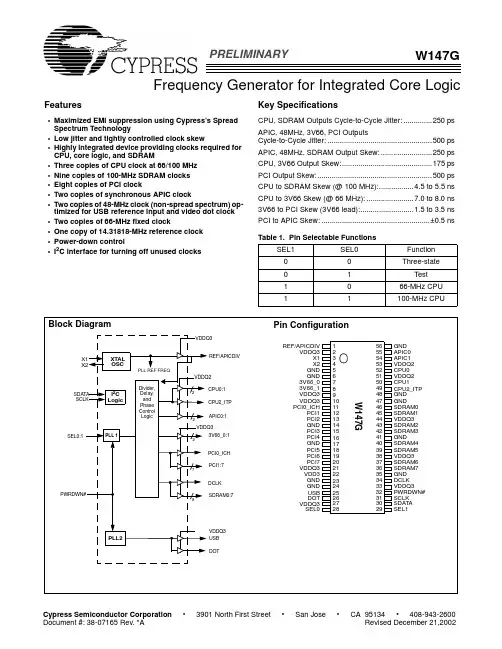
PRELIMINARYFrequency Generator for Integrated Core LogicW147GFeatures•Maximized EMI suppression using Cypress’s Spread Spectrum Technology•Low jitter and tightly controlled clock skew•Highly integrated device providing clocks required for CPU, core logic, and SDRAM•Three copies of CPU clock at 66/100 MHz •Nine copies of 100-MHz SDRAM clocks •Eight copies of PCI clock•Two copies of synchronous APIC clock•Two copies of 48-MHz clock (non-spread spectrum) op-timized for USB reference input and video dot clock •Two copies of 66-MHz fixed clock•One copy of 14.31818-MHz reference clock •Power-down control•I 2C interface for turning off unused clocksKey SpecificationsCPU, SDRAM Outputs Cycle-to-Cycle Jitter:..............250 ps APIC, 48MHz, 3V66, PCI OutputsCycle-to-Cycle Jitter:...................................................500 ps APIC, 48MHz, SDRAM Output Skew:.........................250 ps CPU, 3V66 Output Skew:............................................175 ps PCI Output Skew:........................................................500 ps CPU to SDRAM Skew (@ 100 MHz):.................4.5 to 5.5 ns CPU to 3V66 Skew (@ 66 MHz):.......................7.0 to 8.0 ns 3V66 to PCI Skew (3V66 lead):..........................1.5 to 3.5 ns PCI to APIC Skew:.....................................................±0.5 ns Table 1.Pin Selectable FunctionsSEL1SEL0Function 00Three-state01Test 1066-MHz CPU 11100-MHz CPUPin DefinitionsPin Name Pin No.PinType Pin DescriptionREF/APICDIV1I/O Reference Clock: 3.3V 14.318-MHz clock output. This pin doubles as the selectstrap for APIC clock frequency. If strapped LOW during power up, APIC clock runsat half PCI clock speed. Otherwise, APIC clocks run at PCI clock speed.X13I Crystal Input: This pin has dual functions. It can be used as an external14.318-MHz crystal connection as an external reference frequency input.X24I Crystal Output: An input connection for an external 14.318-MHz crystal. If usingan external reference, this pin must be left unconnected.PCI0_ICH, PCI1:711, 12, 13, 15,16, 18, 19. 20O PCI Clock 0 through 7: 3.3V 33-MHz PCI clock outputs. PCI1:7 can be individually turned off via I2C interface.3V66_0:17, 8O66-MHz Clock Output: 3.3V fixed 66-MHz clock.USB25O USB Clock Output: 3.3V fixed 48-MHz, non-spread spectrum USB clock outputs. DOT26O Dot Clock Output:3.3V 48-MHz, non-spread spectrum signal.SEL0:128, 29I Clock Function Selection pins: LVTTL-compatible input to select device func-tions. See Table 1 for detailed descriptions.PWRDWN#32I Power Down Control: LVTTL-compatible asynchronous input that places the de-vice in power-down mode when held LOW.CPU2_ITP, CPU0:149, 52, 50O CPU Clock Outputs: Clock outputs for the host bus interface and integrated test port. Output frequencies run at 66 MHz or 100 MHz depending on the configurationof SEL0:1. Voltage swing set by V DDQ2.SDRAM0:7, DCLK 46, 45, 43, 42,40, 39, 37, 36,34OSDRAM Clock Outputs: 3.3V outputs running at 100 MHz. SDRAM0:7 can beindividually turned off via I2C interface.APIC0:155, 54O Sychronous APIC Clock Outputs: Clock outputs running divide synchronouswith the PCI clock outputs. Output frequency is controlled by the strap option onREF. Voltage swing set by V DDQ2.SDATA30I/O Data pin for I2C circuitry.SCLK31I Clock pin for I2C circuitry.VDDQ32, 9, 10, 21, 27,33, 38, 44P 3.3V Power Connection: Power supply for SDRAM output buffers, PCI output buffers, 3V66 output buffers, reference output buffers, and 48-MHz output buffers.Connect to 3.3V.VDD322P 3.3V Power Connection: Power supply for core logic, PLL circuitry. Connect to3.3V.VDDQ251, 53P 2.5V Power Connection: Power supply for IOAPIC and CPU output buffers. Con-nect to 2.5V or 3.3V.GND5, 6, 14, 17, 23,24, 35, 41, 47,48, 56G Ground Connections: Connect all ground pins to the common system groundplane.OverviewThe W147G is a highly integrated frequency timing generator,supplying all the required clock sources for an Intel ® architec-ture platform using graphics integrated core logic.Functional DescriptionI/O Pin OperationREF/APICDIV is a dual purpose l/O pin. Upon power-up the pin acts as a logic input. If the pin is strapped to a LOW state externally, APIC clock outputs will run divide synchronously at half PCI clock speed. If it is pulled HIGH, APIC clock will run synchronous to PCI clocks. An external 10-k Ω strapping resis-tor should be used. Figure 1 shows a suggested method for strapping resistor connections.After 2 ms, the pin becomes an output. Assuming the power supply has stabilized by then, the specified output frequency is delivered on the pins. If the power supply has not yet reached full value, output frequency initially may be below tar-get but will increase to target once supply voltage has stabi-lized. In either case, a short output clock cycle may be pro-duced from the CPU clock outputs when the outputs are enabled.Pin Selectable FunctionsTable 1 outlines the device functions selectable through SEL0:1. Specific outputs available at each pin is detailed in Table 2 below. The SEL0 pin requires a 220Ω pull-up resistor to 3.3V for the W147G to sense the maximum host bus fre-quency of the processor and configure itself accordingly.Notes:1.APIC clock frequency determined by the strap option on the REF/APICDIV input pin.2.Provided for board level “bed of nails ” testing.3.“Normal ” mode of operation.4.TCLK is a test clock overdriven on the XTAL_IN input during test mode.5.Required for DC output impedance verification.6.Range of reference frequency allowed is: min. = 14.316 MHz, nominal = 14.31818 MHz, max. = 14.32 MHz.7.Frequency accuracy of 48 MHz must be +167 PPM to match USB default.Power-on Reset TimerOutput Three-stateData LatchHold QDW147G V DDClock Load10 k ΩOutput Buffer(Load Option 1)10k Ω(Load Option 0)Output LowOutput Strapping Resistor Series T ermination ResistorFigure 1.Input Logic Selection Through Resistor Load OptionTable 2.CK Whitney Truth Table SEL1SEL0CPU SDRAM 3V66PCI 48MHz REF APIC [1]Notes 00Hi-Z Hi-Z Hi-Z Hi-Z Hi-Z Hi-Z Hi-Z 201TCLK/2TCLK/2TCLK/3TCLK/6TCLK/2TCLK TCLK/64, 51066 MHz 100 MHz 66 MHz 33 MHz 48 MHz 14.318 MHz 16.67 MHz 3, 6, 711100 MHz100 MHz66 MHz33 MHz48 MHz14.318 MHz16.67 MHz3, 6, 7Offsets Among Clock Signal GroupsFigure 2 and Figure 3 represent the phase relationship among the different groups of clock outputs from W147G when it is providing a 66-MHz CPU clock and a 100-MHz CPU clock,respectively. It should be noted that when CPU clock is oper-ating at 100 MHz, CPU clock output is 180 degrees out of phase with SDRAM clock outputs.CPU 66-MHz3V66 66-MHzPCI 33-MHzUSB 48-MHzAPIC 33-MHzFigure 2.Group Offset Waveforms (66-MHz CPU Clock) CPU 100-MHz3V66 66-MHzPCI 33-MHzUSB 48-MHzAPIC 33-MHzFigure 3.Group Offset Waveforms (100-MHz CPU Clock)Power Down ControlW147G provides one PWRDWN# signal to place the device in low-power mode. In low-power mode, the PLLs are turned off and all clock outputs are driven LOW.8.Once the PWRDWN# signal is sampled LOW for two consecutive rising edges of CPU clock, clocks of interest should be held LOW on the next HIGH-to-LOWtransition.9.PWR_DWN# is an asynchronous input and metastable conditions could exist. This signal is synchronized inside W147G.10.The shaded sections on the SDRAM, REF, and USB clocks indicate “don ’t care ” states.11.Diagrams shown with respect to 100 MHz. Similar operation when CPU is 66 MHz.Table 3.W147G Maximum Allowed CurrentW147 ConditionMax. 2.5V supply consumptionMax. discrete cap loads,V DDQ2 = 2.625VAll static inputs = V DDQ3 or V SSMax. 3.3V supply consumptionMax. discrete cap loadsV DDQ3 = 3.465VAll static inputs = V DDQ3 or V SSPowerdown Mode (PWRDWN# = 0)100 µA 200 µA Full Active 66 MHzSEL1,0 = 10 (PWRDWN# =1)70 mA 280 mA Full Active 100 MHzSEL1,0 =11 (PWRDWN# = 1)100 mA280 mASpread Spectrum ClockingThe device generates a clock that is frequency modulated in order to increase the bandwidth that it occupies. By increasing the bandwidth of the fundamental and its harmonics, the am-plitudes of the radiated electromagnetic emissions are re-duced. This effect is depicted in Figure 5.As shown in Figure 5, a harmonic of a modulated clock has a much lower amplitude than that of an unmodulated signal. The reduction in amplitude is dependent on the harmonic number and the frequency deviation or spread. The equation for the reduction isdB = 6.5 + 9*log 10(P) + 9*log 10(F)Where P is the percentage of deviation and F is the frequency in MHz where the reduction is measured.The output clock is modulated with a waveform depicted in Figure 6. This waveform, as discussed in “Spread Spectrum Clock Generation for the Reduction of Radiated Emissions ” by Bush, Fessler, and Hardin produces the maximum reduction in the amplitude of radiated electromagnetic emissions. The deviation selected for this chip is –0.5% of the selected fre-quency. Figure 6 details the Cypress spreading pattern.Cypress does offer options with more spread and greater EMI reduction. Contact your local Sales representative for details on these devices.Spread Spectrum clocking is activated or deactivated by se-lecting the appropriate value for bit 3 in data byte 0 of the I 2C data stream. Refer to page 8 for more details.Spread Spectrum EnabledEMI ReductionSpread SpectrumNon-Figure 5.Typical Clock and SSFTG ComparisonMAX.MIN.F R E Q U E N C YFigure 6.Typical Modulation ProfileSerial Data InterfaceThe W147G features a two-pin, serial data interface that can be used to configure internal register settings that control par-ticular device functions. Data ProtocolThe clock driver serial protocol accepts only block writes from the controller. The bytes must be accessed in sequential order from lowest to highest byte with the ability to stop after any complete byte has been transferred. Indexed bytes are not allowed.A block write begins with a slave address and a write condition.After the command code the core logic issues a byte count which describes how many more bytes will follow in the mes-sage. If the host had 20 bytes to send, the first byte would be the number 20 (14h), followed by the 20 bytes of data. The byte count may not be 0. A block write command is allowed to transfer a maximum of 32 data bytes. The slave receiver ad-dress for W147G is 11010010. Figure 7 shows an example of a block write.The command code and the byte count bytes are required as the first two bytes of any transfer. W147G expects a command code of 0000 0000. The byte count byte is the number of ad-ditional bytes required for the transfer, not counting the com-mand code and byte count bytes. Additionally, the byte count byte is required to be a minimum of 1 byte and a maximum of 32 bytes to satisfy the above requirement. Table 4 shows an example of a possible byte count value.A transfer is considered valid after the acknowledge bit corre-sponding to the byte count is read by the controller. The com-mand code and byte count bytes are ignored by the W147G.However, these bytes must be included in the data write se-quence to maintain proper byte allocation.Notes:12.The acknowledgment bit is returned by the slave/receiver (W147G).13.Data Bytes 3 to 7 are reserved.1 bit 7 bits 118 bits 1Start bitSlave AddressR/WAckCommand CodeAckByte Count = NAck Data Byte 1Ack Data Byte 2Ack ...Data Byte N Ack Stop 1 bit8 bits18 bits18 bits11Figure 7.An Example of a Block Write [12]Table 4.Example of Possible Byte Count ValueByte Count Byte NotesMSB LSB 00000000Not allowed. Must have at least one byte.00000001Data for functional and frequency select register (currently byte 0 in spec)00000010Reads first two bytes of data. (byte 0 then byte 1)00000011Reads first three bytes (byte 0, 1, 2 in order)00000100Reads first four bytes (byte 0, 1, 2, 3 in order)00000101Reads first five bytes (byte 0, 1, 2, 3, 4 in order)[13]00000110Reads first six bytes (byte 0, 1, 2, 3, 4, 5 in order)[13]00000111Reads first seven bytes (byte 0, 1, 2, 3, 4, 5, 6 in order)00100000Max byte count supported = 32Table 5.Serial Data Interface Control Functions Summary Control Function DescriptionCommon ApplicationOutput DisableAny individual clock output(s) can be disabled. Disabled outputs are actively held LOW.Unused outputs are disabled to reduce EMI and sys-tem power. Examples are clock outputs to unused PCI slots.Spread Spectrum Enabling Enables or disables spread spectrum clocking.For EMI reduction.(Reserved)Reserved function for future device revision or pro-duction device testing.No user application. Register bit must be written as 0.W147G Serial Configuration Map1.The serial bits will be read by the clock driver in the following order:Byte 0 - Bits 7, 6, 5, 4, 3, 2, 1, 0Byte 1 - Bits 7, 6, 5, 4, 3, 2, 1, 0Byte N - Bits 7, 6, 5, 4, 3, 2, 1, 02.All unused register bits (reserved and N/A) should be writ-ten to a “0” level.3.All register bits labeled “Initialize to 0" must be written to zero during initialization. Failure to do so may result in high-er than normal operating current.4.Only Byte 0, 1 and 2 are defined in W147G Byte 3 to Byte 7 are reserved and must be written to “zero.”14.Inactive means outputs are held LOW and are disabled from switching. These outputs are designed to be configured at power-on and are not expected to beconfigured during the normal modes of operation.Byte 0: Control Register (1 = Enable, 0= Disable)[14]BitPin#NamePin DescriptionBit 7-Reserved (Active/Inactive)Bit 6-Reserved (Active/Inactive)Bit 5-Reserved (Active/Inactive)Bit 4-Reserved(Active/Inactive)Bit 3-Spread Spectrum (1=On/0=Off)(Active/Inactive)Bit 226DOT (Active/Inactive)Bit 125USB (Active/Inactive)Bit 049CPU2_ITP(Active/Inactive)Byte 1: Control Register (1 = Enable, 0= Disable)[14]BitPin#NamePin DescriptionBit 736SDRAM7(Active/Inactive)Bit 637SDRAM6(Active/Inactive)Bit 539SDRAM5(Active/Inactive)Bit 440SDRAM4(Active/Inactive)Bit 342SDRAM3(Active/Inactive)Bit 243SDRAM2(Active/Inactive)Bit 145SDRAM1(Active/Inactive)Bit 046SDRAM0(Active/Inactive)Byte 2: Control Register (1 = Enable, 0= Disable)[14]BitPin#NamePin DescriptionBit 720PCI7(Active/Inactive)Bit 619PCI6(Active/Inactive)Bit 518PCI5(Active/Inactive)Bit 416PCI4(Active/Inactive)Bit 315PCI3(Active/Inactive)Bit 213PCI2(Active/Inactive)Bit 112PCI1(Active/Inactive)Bit 0-Reserved(Active/Inactive)DC Electrical Characteristics [15]DC parameters must be sustainable under steady state (DC) conditions.Note:15.Multiple Supplies: The voltage on any input or I/O pin cannot exceed the power pin during power-up. Power supply sequencing is NOT required. 16.Input Leakage Current does not include inputs with pull-up or pull-down resistors.Absolute Maximum DC Power SupplyParameter DescriptionMin.Max.Unit V DD3 3.3V Core Supply Voltage –0.5 4.6V V DDQ2 2.5V I/O Supply Voltage –0.5 3.6V V DDQ3 3.3V Supply Voltage –0.5 4.6V T SStorage Temperature–65150°CAbsolute Maximum DC I/OParameter DescriptionMin.Max.Unit V ih3 3.3V Input High Voltage –0.5 4.6V V il3 3.3V Input Low Voltage –0.5V ESD prot.Input ESD Protection2000VDC Operating RequirementsParameter DescriptionCondition Min.Max.Unit V DD3 3.3V Core Supply Voltage 3.3V±5% 3.135 3.465V V DDQ3 3.3V I/O Supply Voltage 3.3V±5% 3.135 3.465V V DDQ22.5V I/O Supply Voltage2.5V±5%2.3752.625VV DD3 = 3.3V±5%V ih3 3.3V Input High Voltage V DD32.0V DD +0.3V V il33.3V Input Low Voltage V SS –0.30.8V I ilInput Leakage Current [16]0<V in <V DDQ3–5+5µAV DDQ2 = 2.5V±5%V oh2 2.5V Output High Voltage I oh =(–1 mA) 2.0V V ol22.5V Output Low VoltageI ol =(1 mA)0.4VV DDQ3 = 3.3V±5%V oh3 3.3V Output High Voltage I oh =(–1 mA) 2.4V V ol33.3V Output Low VoltageI ol =(1 mA)0.4VV DDQ3 = 3.3V±5%V poh3PCI Bus Output High Voltage I oh =(–1 mA) 2.4V V pol3PCI Bus Output Low Voltage I ol =(1 mA)0.55V C in Input Pin Capacitance 5pF C xtal Xtal Pin Capacitance 13.522.5pF C out Output Pin Capacitance 6pF L pin Pin Inductance 07nH T aAmbient TemperatureNo Airflow070°CAC Electrical Characteristics [15]T A = 0°C to +70°C, V DDQ3 = 3.3V±5%, V DDQ2= 2.5V±5%f XTL = 14.31818 MHzSpread Spectrum function turned offAC clock parameters are tested and guaranteed over stated operating conditions using the stated lump capacitive load at the clock output.[17]Notes:17.Period, jitter, offset, and skew measured on rising edge at 1.25 for 2.5V clocks and at 1.5V for 3.3V clocks.18.T HIGH is measured at 2.0V for 2.5V outputs, 2.4V for 3.3V outputs.19.T LOW is measured at 0.4V for all outputs.20.The time specified is measured from when V DDQ3 achieves its nominal operating level (typical condition V DDQ3 = 3.3V) until the frequency output is stable andoperating within specification.21.T RISE and T FALL are measured as a transition through the threshold region V ol = 0.4V and V oh = 2.0V (1 mA) JEDEC specification.Parameter Description66.6-MHz Host100-MHz Host Unit Notes Min.Max.Min.Max.T Period Host/CPUCLK Period 15.015.510.010.5ns 17T HIGH Host/CPUCLK High Time 5.2N/A 3.0N/A ns 20T LOW Host/CPUCLK Low Time 5.0N/A 2.8N/A ns 21T RISE Host/CPUCLK Rise Time 0.4 1.60.4 1.6ns T FALL Host/CPUCLK Fall Time 0.4 1.60.4 1.6ns T Period SDRAM CLK Period 10.010.510.010.5ns 17T HIGH SDRAM CLK High Time 3.0N/A 3.0N/A ns 20T LOW SDRAM CLK Low Time 2.8N/A 2.8N/A ns 21T RISE SDRAM CLK Rise Time 0.4 1.60.4 1.6ns T FALL SDRAM CLK Fall Time 0.4 1.60.4 1.6ns T Period APIC CLK Period 60.064.060.064.0ns 17T HIGH APIC CLK High Time 25.5N/A 25.5N/A ns 20T LOW APIC CLK Low Time 25.3N/A 25.3N/A ns 21T RISE APIC CLK Rise Time 0.4 1.60.4 1.6ns T FALL APIC CLK Fall Time 0.4 1.60.4 1.6ns T Period 3V66 CLK Period 15.016.015.016.0ns 17, 19T HIGH 3V66 CLK High Time 5.25N/A 5.25N/A ns 20T LOW 3V66 CLK Low Time 5.05N/A 5.05N/A ns 21T RISE 3V66 CLK Rise Time 0.5 2.00.5 2.0ns T FALL 3V66 CLK Fall Time 0.5 2.00.5 2.0ns T Period PCI CLK Period 30.0N/A 30.0N/A ns 17, 18T HIGH PCI CLK High Time 12.0N/A 12.0N/A ns 20T LOW PCI CLK Low Time 12.0N/A 12.0N/A ns 21T RISE PCI CLK Rise Time 0.5 2.00.5 2.0ns T FALL PCI CLK Fall Time0.5 2.00.5 2.0ns tp ZL , tp ZH Output Enable Delay (All outputs) 1.010.0 1.010.0ns tp LZ , tp ZH Output Disable Delay (All outputs) 1.010.0 1.010.0ns t stableAll Clock Stabilization from Power-Up33msDocument #: 38-07165 Rev. *A Page 11 of 13Intel is a registered trademark of Intel Corporation.Group Skew and Jitter Limits Output GroupPin-Pin Skew MaxCycle-Cycle JitterDuty Cycle Nom Vdd Skew, Jitter Measure PointCPU 175 ps 250 ps 45/55 2.5V 1.25V SDRAM 250 ps 250 ps 45/55 3.3V 1.5V APIC 250 ps 500 ps 45/55 2.5V 1.25V 48MHz 250 ps 500 ps 45/55 3.3V 1.5V 3V66175 ps 500 ps 45/55 3.3V 1.5V PCI 500 ps 500 ps 45/55 3.3V 1.5V REFN/A1000 ps45/553.3V1.5V2.5V Clocking3.3V Clocking RISEFALLInterfaceInterfaceFigure 8.Output BufferOrdering InformationOrdering Code Package NamePackage TypeW147GH56-pin SSOP (300 mils)Document #: 38-07165 Rev. *A Page 12 of 13© Cypress Semiconductor Corporation, 2001. The information contained herein is subject to change without notice. Cypress Semiconductor Corporation assumes no responsibility for the use of any circuitry other than circuitry embodied in a Cypress Semiconductor product. Nor does it convey or imply any license under patent or other rights. Cypress Semiconductor does not authorize its products for use as critical components in life-support systems where a malfunction or failure may reasonably be expected to result in significant injury to the user. The inclusion of Cypress Semiconductor products in life-support systems application implies that the manufacturer assumes all risk of such use and in doing so indemnifies Cypress Semiconductor against all charges.Package Diagram56-Pin Shrink Small Outline Package (SSOP , 300 mils)Summary of nominal dimensions in inches:Body Width: 0.296Lead Pitch: 0.025Body Length: 0.625Body Height: 0.102Document #: 38-07165 Rev. *A Page 13 of 13Document Title: W147G Frequency Generator for Integrated Core Logic Document Number: 38-07165REV.ECN NO.Issue Date Orig. of Change Description of Change**11027511/05/01SZV Change from Spec number: 38-00820 to 38-07165*A12280612/21/02RBIAdd Power up Requirements to Operating Conditions Information。